Article

A Circularly Polarized Antenna Array with Gain Enhancement for Long-Range UHF RFID Systems

1
School of Information and Communication Engineering, University of Electronics Science and Technology of China, Chengdu 611731, China
2
School of Electronic Science and Engineering, University of Electronics Science and Technology of China, Chengdu 611731, China
3
Department of Electrical and Computer Engineering, Dalhousie University, Halifax, NS B3H 4R2, Canada
4
College of Physics and Information Engineering, Fuzhou University, Fuzhou 350108, China
*
Authors to whom correspondence should be addressed.
Electronics 2019, 8(4), 400; https://doi.org/10.3390/electronics8040400
Submission received: 18 February 2019 / Revised: 29 March 2019 / Accepted: 29 March 2019 / Published: 3 April 2019
(This article belongs to the Special Issue Recent Advances in Array Antenna and Array Signal Processing)

Abstract

:
A 2 × 2 circularly polarized (CP) sequential rotation microstrip patch antenna array with high gain for long-range ultra-high frequency (UHF) radio frequency identification (RFID) communication is proposed in this paper. In order to meet the operational frequency band requirement of 840–960 MHz and, at the same time, achieve enhanced broadside gain, a two-level sequential rotation structure is developed. Series power divider is used as the basic element of the feed network that is implemented with the substrate-integrated coaxial line technology for minimizing radiation losses. The manufactured prototype exhibits a peak gain of 12.5 dBic at 900 MHz and an axial ratio (AR) bandwidth (AR ≤ 3 dB) of 18.2% from 828 to 994 MHz. In comparison with the state-of-the-art, the proposed antenna shows an excellent gain/size trade-off.

1. Introduction

Wireless communication technologies, nowadays, advance and diffuse quickly, and they are continuously evolving towards smaller devices with fewer energy requirements. This evolution is recently driven by the concept of “Internet-of-Things” (IoT), which aims at the development of ultra-dense networks, even if energy consumption is still an issue. In this sense, radio frequency identification (RFID) is a well-consolidated technology and a good candidate for the implementation of some IoT devices [1]. However, today’s RFID solutions are still limited in terms of communication range. In the case of a monostatic RFID, the maximum achievable communication range r in an ideal case of line-of-sight propagation (and under the hypothesis of perfect antennas alignment and no polarization mismatch) is governed by the link budget equations (expressed in dB) [2]:
{ P f o r w a r d = P E I R P + G t a g + 20 log 10 ( λ 4 π r ) P t h , t a g P b a c k = P f o r w a r d + G r e a d e r + G t a g + 20 log 10 ( λ 4 π r ) + 10 log 10 ( M ) P t h , r e a d e r ,
where Pforward and Pback are the forward link received power (from reader to tag) and the backward link received power (from tag to reader) in dBm, respectively; PEIRP (dBm) is the effective isotropic radiated power (whose maximum value is fixed by communication standards), Greader and Gtag (expressed in dBi) are the reader and tag antenna gains, respectively; M is the modulation factor; Pth,tag and Pth,reader are the sensitivities (expressed in dBm) of the tag and the reader, respectively; and λ is the wavelength. One possibility to increase the communication range is the reduction of the two sensitivities, which is a natural process driven by the technological evolution. Furthermore, the use of semi-passive or active tag devices (which can improve the tag sensitivity or increase the factor M) is also beneficial [1,3], but requires an increased amount of energy. Finally, the capability to radiate circular polarization (CP) [4] for immunity to polarization mismatching and resistance to multipath effects [5] is of fundamental importance for maximizing the communication range.
From Equation (1), however, it is clear that for long-range RFID communication, high-gain antennas have to be employed. In particular, not only is the reader antenna gain Greader fundamental to extend the backward link range, but its enhancement can contribute significantly to a transmitting power reduction (since PEIR P = Ptx + Greader) without affecting the forward link range.
Many studies have been conducted to achieve high-gain RFID reader antennas which can cover the universal ultra-high frequency (UHF) RFID band [6,7,8,9]. A maximum CP gain of 9.3 dBic is demonstrated in [7] with a single antenna configuration and the use of a structure with a high profile (35 mm).
To further increase the antenna gain, an array structure can be employed. In addition, the sequential rotation (SR) technique [10] has also been used effectively in many different cases because of its capability to radiate CP and provide high gain and wide bandwidth [11,12,13]. An example of SR antenna array for high-gain RFID readers is reported in [11], which exhibits a gain of about 12.3 dBic, but with a relatively large size of 590 × 590 × 1.524 mm3 (1.8 × 1.8 × 0.005 λ3). Similar or higher-gain antennas can be obtained at the expense of an increased design complexity, such as a complex feed network [12] and a metasurface [13].
In this manuscript, a 2 × 2 SR antenna array with high-gain characteristics for long-range UHF RFID systems is developed. Similar to [14] (where the objective was, however, the feed network optimization for achieving wideband axial ratio (AR) with ≤1 dB performance), a two-level SR feed network using series power dividers was implemented. Series-fed arrays have been already proposed in the literature [15,16], but in this case, the series configuration was employed to implement the SR method. Moreover, the feed network was designed with substrate-integrated coaxial line (SICL) technology [17,18,19]. It is shown that the two-level SR feed network implemented with SICL technology not only guarantees the achievement of an enhanced gain performance with respect to one-level configuration (or with respect to microstrip technology feed network because of a reduced insertion loss), but also minimizes the gain degradation within the working bandwidth, yielding to a wider 3 dB gain bandwidth. The microstrip patch height and array interelement distance were optimized to maximize the gain and guarantee the required bandwidth. A prototype was fabricated with a size of 440 × 440 × 22.5 mm3 (1.32 × 1.32 × 0.068 λ3), and the measurement results show a peak gain of 12.5 dBic, and an overlapped bandwidth (defined as the spectrum portion in which |S11| ≤ −10 dB impedance bandwidth, AR bandwidth, and 3 dB gain bandwidth overlap) of 18.2% (828–994 MHz), which covers the universal UHF RFID 840–960 MHz bandwidth). Furthermore, even if not experimentally proven, it is shown that better peak gain performance can be achieved at the expense of a bandwidth reduction.
A comparison with other existing high-gain wideband CP antenna arrays reveals that the proposed antenna offers an excellent trade-off between gain and antenna size, also demonstrated by comparing the theoretical limits of antennas in terms of Q-factor and aperture efficiency.

2. The Proposed Antenna Design

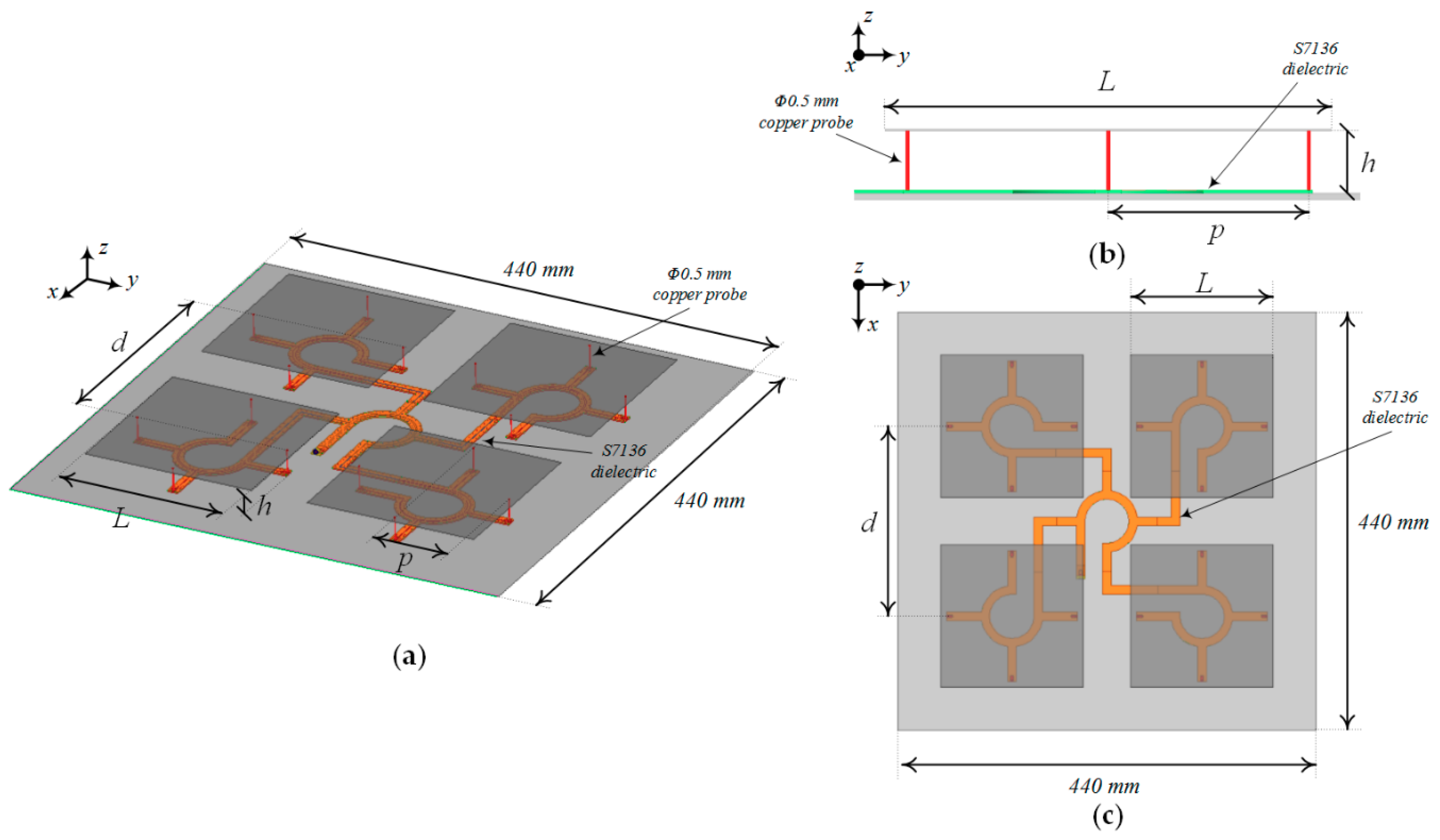
2.1. Antenna Structure

The structure of the antenna array is shown in Figure 1. A 2 × 2 array configuration was realized by employing four probe-fed square microstrip patch antennas with a center-to-center distance d = 0.6λ (λ calculated at 900 MHz), and a 2 mm-thick aluminum ground plane of size 440 × 440 mm2 (a thick ground plane is employed for increasing the structure robustness). Each microstrip patch antenna was implemented with an air gap of height h = 20 mm and an upper 0.5 mm-thick square aluminum patch of edge length L = 150 mm. An SICL-based feed network was implemented with an S7136 dielectric substrate (εR = 3.6, tanδ = 0.0035) fixed on the top side of the ground plane. The feed network substrate did not cover the whole ground plane and was shaped to follow the route of the feed network transmission line. Each antenna element was connected to the feed network through four metallic cylindrical probes of diameter 0.5 mm, positioned at a distance p = 67.5 mm from the element center point, to implement a four-probe microstrip patch antenna structure which was employed to radiate CP, as will be better described in the next section. Finally, Teflon screws were used to support the aluminum patches (not shown in Figure 1).

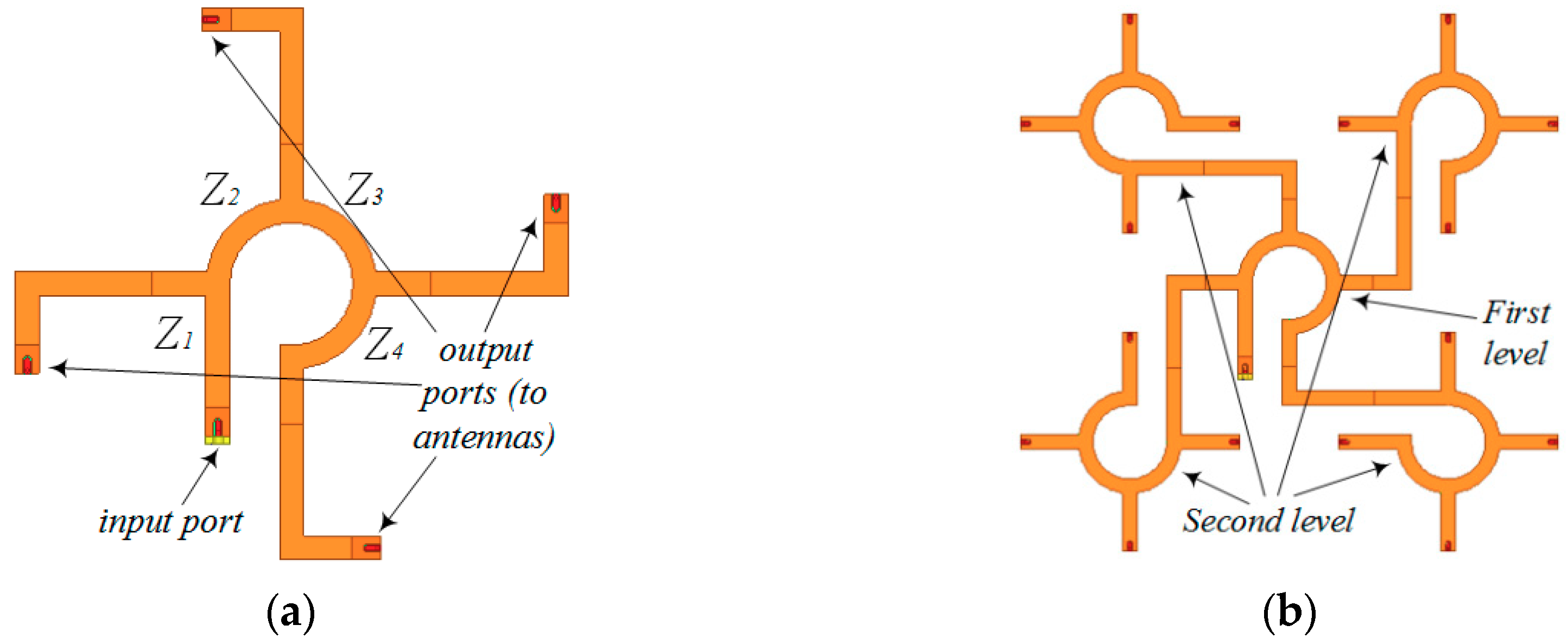
2.2. Sequential Rotated Feed Network

In order to obtain CP radiation, the SR technique [10] was implemented. A series power divider was designed according to [20] but with SICL technology, and used as the feed network basic element to achieve equal amplitude signals and orthogonal phases as required by the SR method. It was implemented as the cascade of four quarter-wave transformer lines with characteristic impedances Z1, Z2, Z3, and Z4, respectively (see Figure 2a). Since each antenna was designed to exhibit an input impedance of 50 Ω, the four characteristic impedances of the feed line sections were Z1 = 25 Ω, Z2 = 16.7 Ω, Z3 = 25 Ω, and Z4 = 50 Ω, respectively, guaranteeing both impedance-matching and equal power distribution [19]. As the feed signal propagated clockwise, left-handed CP (LHCP) radiation was formed in the z > 0 plane.
One- and two-level SR feed networks were designed with SICL technology and compared: the one-level feed network shown in Figure 2a was implemented with a central series power divider, where each output port was used to feed one patch antenna. On the other hand, the two-level feed network represented in Figure 2b was designed by cascading each output port of the central series divider with another series divider (called an “element series divider” hereafter). Each element series divider was used to feed one patch antenna, as shown in Figure 1.
By employing the one and two levels of SR implemented with SICL technology, two antenna arrays were designed: the first employs four linearly polarized (LP) patch antennas, each of them fed by one of the series power divider output ports in Figure 2a (obviously, although each antenna element is LP, the use of the SR feed network guarantees the generation of CP); the second array also employs four patch antennas, but each of them is fed by the four output ports of the element series divider of the two-level SR feed network in Figure 2b, connected to four orthogonal points as can be seen in Figure 1a. Simulated performance of the two antenna arrays were compared in Figure 3 in terms of S11, AR, and LHCP broadside gain. Simulation results were obtained with the software ANSYS HFSS 15.0.0.
As expected, the two-level SR feed network exhibits improved performance over the one-level SR feed network antenna array. In particular, S11 and AR bandwidths widen considerably by applying the second level of SR, as already seen in [14]. Furthermore, since with the one-level SR feed network the antenna elements are LP, while with the two-level SR feed network the antenna elements are CP (thanks to the presence of the element series divider), there is a gain enhancement of about 3 dB in terms of maximum value [21]. Finally, the S11/AR bandwidth widening causes a general gain enhancement within the whole bandwidth, yielding to a wider 3 dB gain bandwidth.

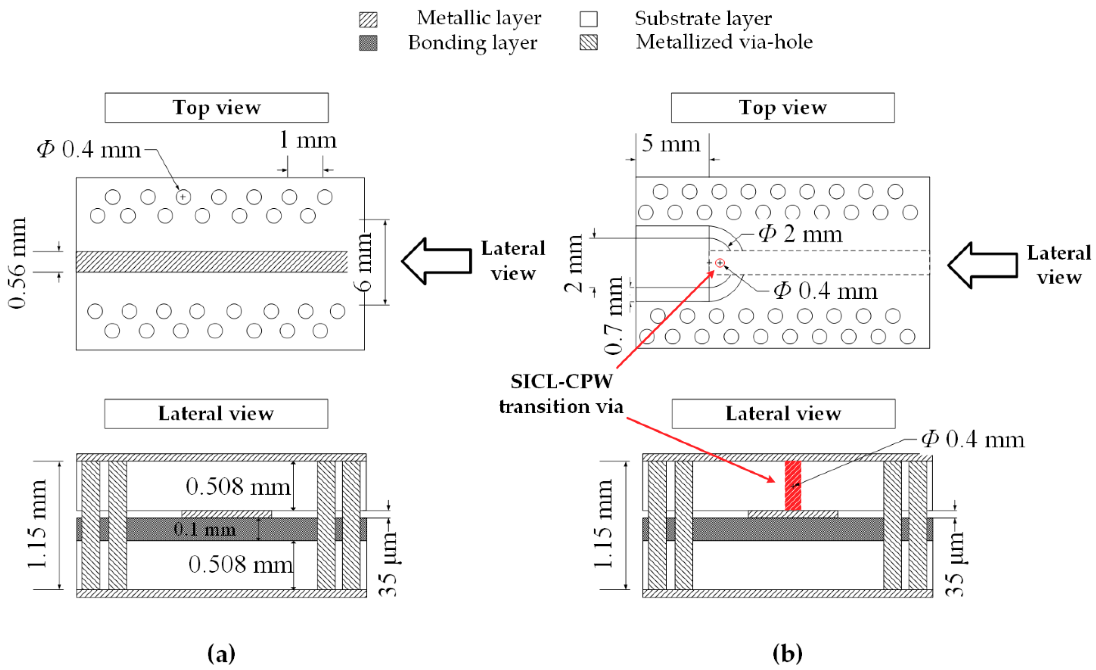
2.3. SICL-Based Feed Network

SICL technology [15] was chosen for the implementation of the antenna array feed network. This is a non-disperse structure which can propagate the transverse electromagnetic (TEM) mode.
The lateral shielding due to the metallic holes (Figure 4) avoids parallel-plate mode propagation, reducing leakage and interference with other lines. Moreover, SICL can be implemented using the conventional multilayer printed circuit board (PCB). For the sake of an easier connection between the metallic patch and the feed network transmission line, a coplanar waveguide (CPW) transition [22] was introduced at each output port of the feed network. Feed network dimensions were synthesized according to [15] and optimized with ANSYS HFSS.
The simulated performance was compared with that of a microstrip technology-based feed network (similar to the one described in [23]), and the results are shown in Figure 5. Wider S11 and AR bandwidths were found for the SICL-based array, with a gain enhancement of about 1 dB with respect to the microstrip-based feed network, and a wider 3 dB gain bandwidth.

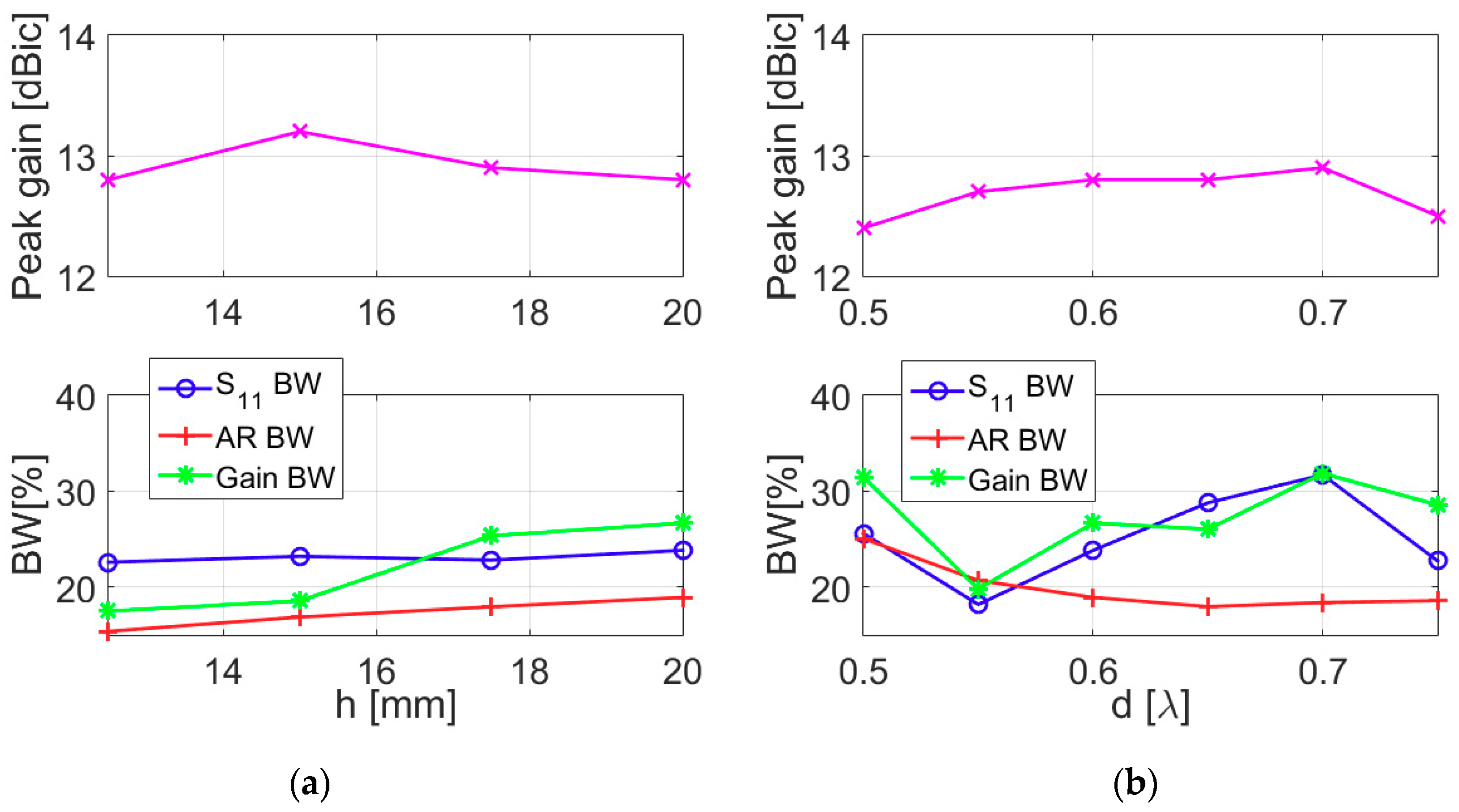
2.4. Microstrip Patch Antenna Height (h)

Antenna array performance was also optimized by appropriately selecting the patch antenna height h. In fact, it is known that the higher the h, the broader the bandwidth and the larger the gain [24]. However, it is also known that if the patch antenna height meets the following condition [25],
h > λ 0.3 2 π ε r ,
surface wave modes become significant and reduce the broadside gain. For this reason, a trade-off between the gain enhancement and the bandwidth needs to be made. Parametric study on the patch antenna height h was conducted as shown in Figure 6a (for each value of h, the antenna length L and the feed probe position p has been optimized to resonate at the same frequency). As can be seen after Equation (2) is satisfied, the gain starts to decrease slightly, but the bandwidth still continues to widen. We have selected the value h = 20 mm as a good compromise between gain and bandwidth (the gain is only 0.3 dB less than its maximum value, with an overlapped bandwidth wider than 18%, where the overlapped bandwidth is defined as the spectrum portion in which |S11| ≤ −10 dB impedance bandwidth, AR bandwidth, and 3 dB gain bandwidth overlap).

2.5. Antenna Array Element Distance (d)

Finally, a parametric study on the array element distance d was conducted. In fact, an increase of d reduced the mutual coupling among antenna elements, leading to a broadside gain enhancement; however, large d can cause the generation of grating lobes and the presence of border effects (because the metallic patch position is close to the ground plane edge) with a consequent reduction of the gain. For this reason, the parameter d was varied from 0.5λ to 0.75λ, and simulation results are depicted in Figure 6b. The increase of d is beneficial for gain enhancement (in terms of peak value and bandwidth) up to a value of 0.7λ. Interestingly, peak gain and bandwidth mainly follow the S11 bandwidth behavior (revealing that, in this case, gain enhancement is mainly due to improved impedance-matching performance), while AR bandwidth exhibits an opposite trend. As for h, a trade-off between LHCP broadside gain and AR bandwidth was made, and a final value d = 0.6λ was selected.

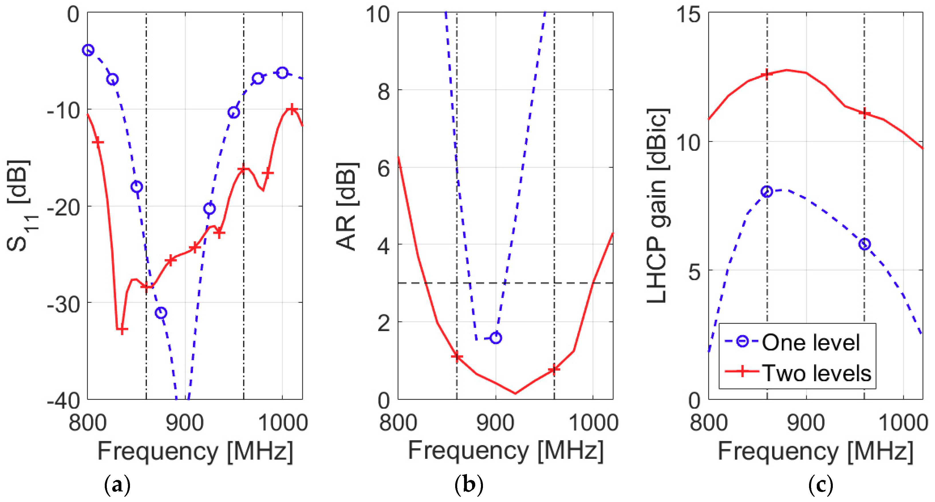
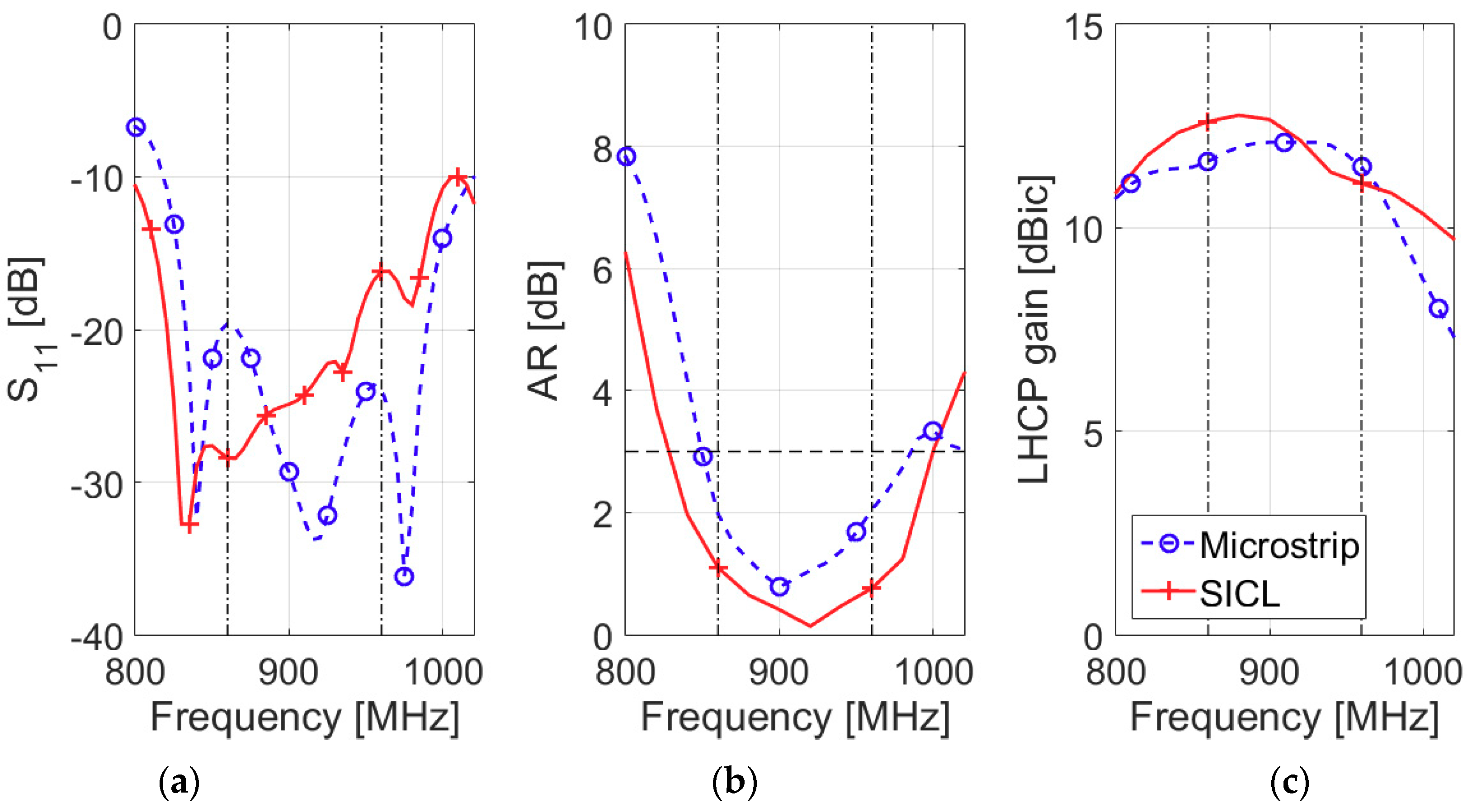
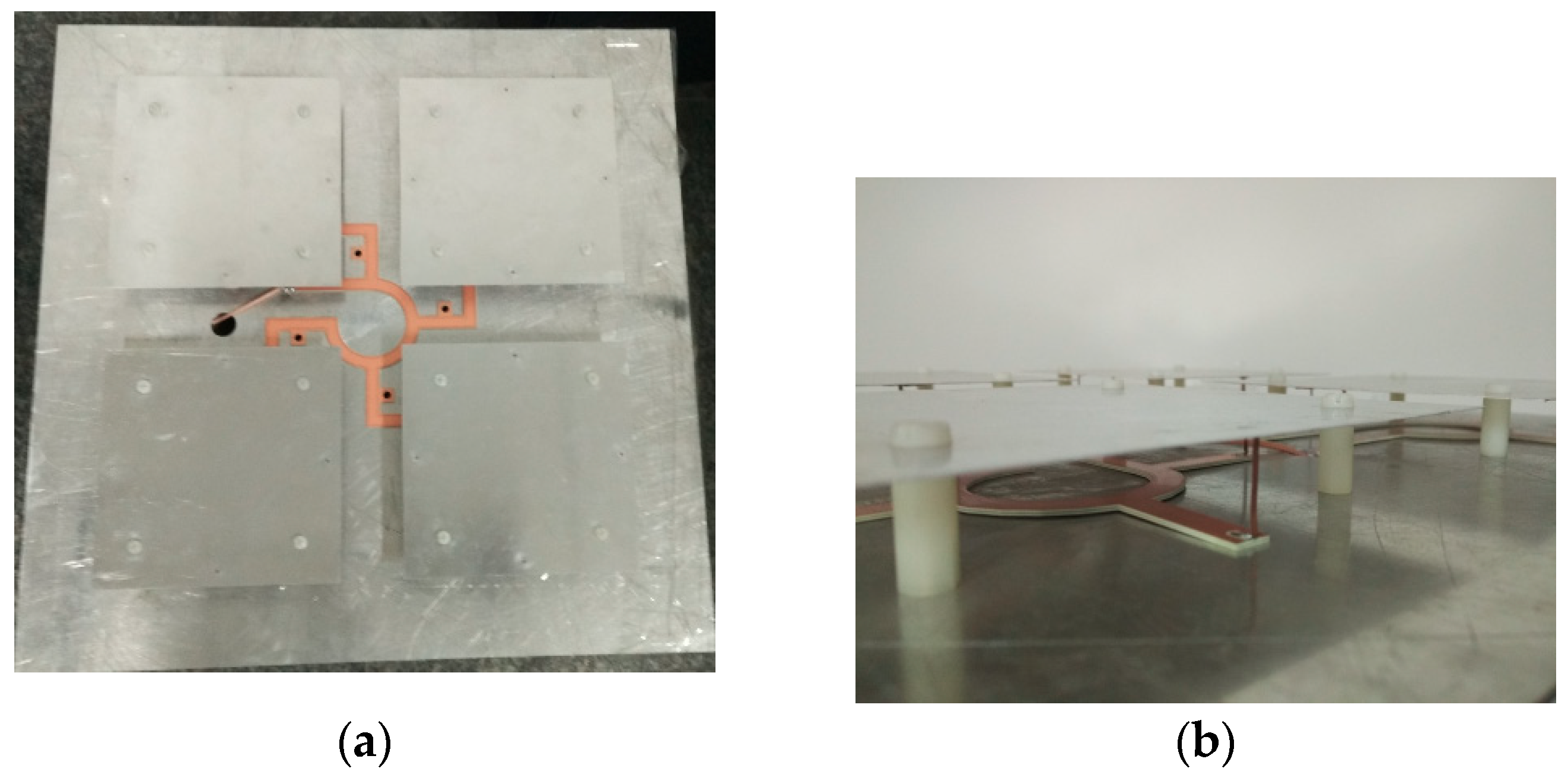
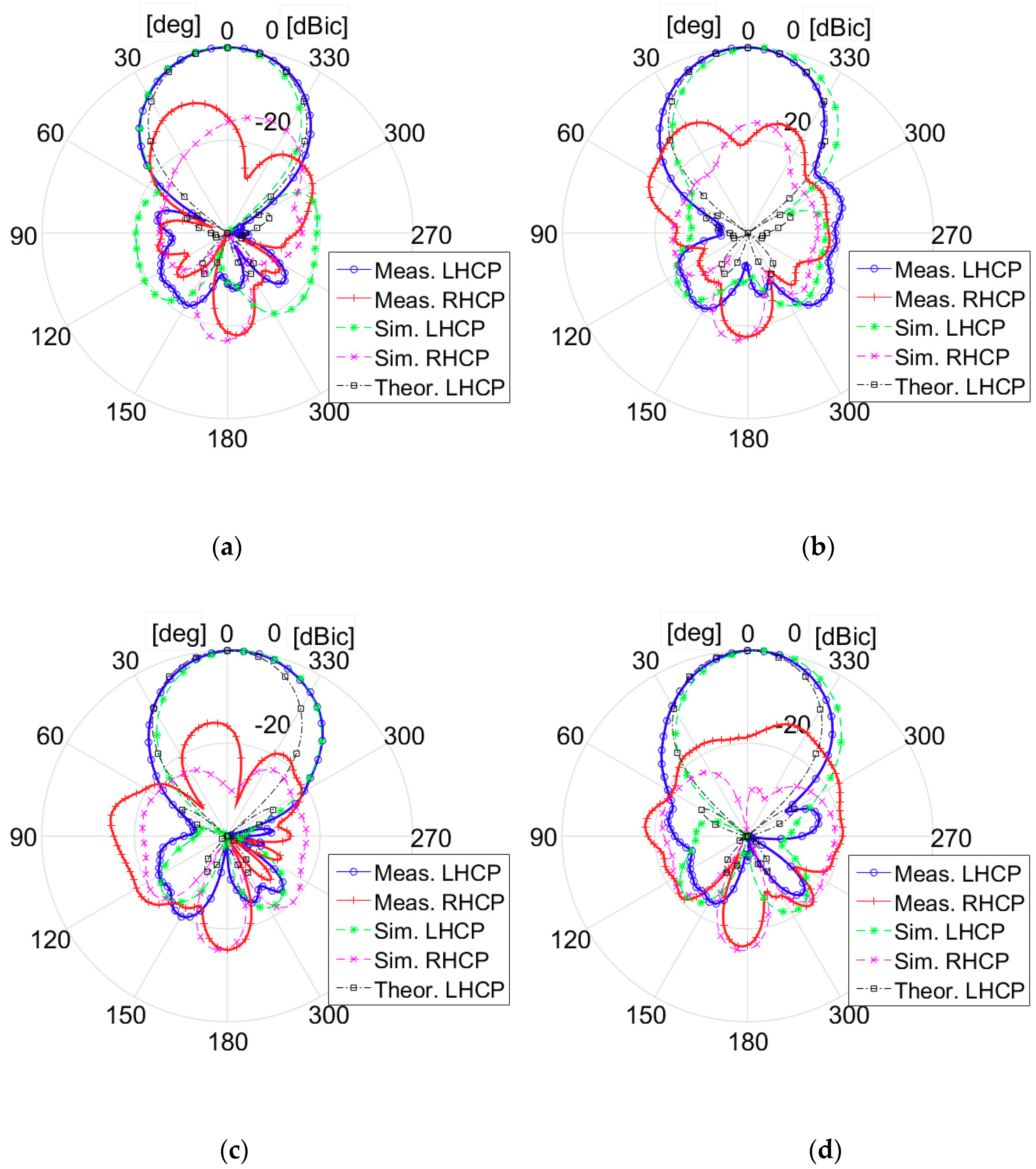
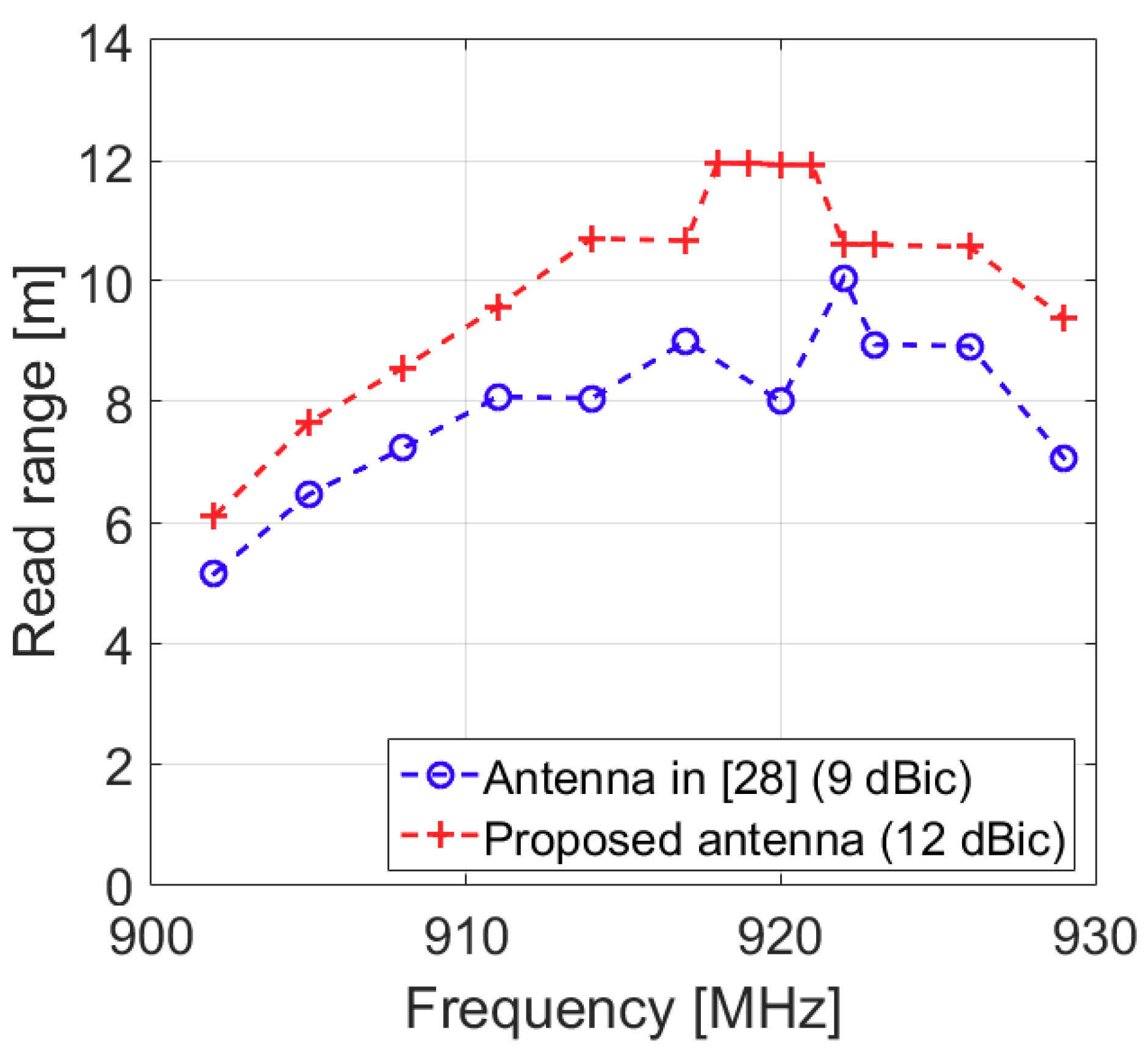
3. Measurement Results and Discussion

A prototype of the 2 × 2 antenna array, depicted in Figure 7, was manufactured for verification. In particular, S11 was measured with a vector network analyzer (Agilent N5230A, Agilent Technologies, Santa Clara, CA, United States), while far-field behavior was verified in an anechoic chamber. Specifically, antenna gain was determined by comparing the antenna’s gain with that of a standard horn antenna, while AR was calculated from right-handed CP (RHCP) and LHCP electric field components as in [26].
Comparisons of ANSYS HFSS results and measured S11, AR, and LHCP gain, and the simulated (with HFSS) radiation efficiency are shown in Figure 8 (only the bandwidth from 780 to 1020 MHz is depicted for the sake of representation clarity). An |S11|≤ −10 dB bandwidth from 759 to 1026 MHz (29.9%) was observed. Furthermore, AR ≤ 3 dB was obtained within the frequency band of 828–994 MHz (18.2%), which covers the target band of 840–960 MHz. Finally, a peak gain value of 12.5 dBic at the frequency 900 MHz, a 3 dB gain bandwidth broader than 26.3% (800–1030 MHz), and a simulated efficiency larger than 82.7% within the bandwidth 840–960 MHz were obtained.
Few discrepancies between the measurement and simulation results were observed, probably due to manufacturing tolerances, dielectric material parameter variations, and simulation and test errors.
Measured and simulated radiation patterns for the frequencies 870 and 930 MHz were plotted, in Figure 9, for both xz- and yz-planes (only two frequencies are shown for brevity), while AR ≤ 3 dB beamwidths are listed in Table 1 for the frequencies 840, 900, and 960 MHz.
The measured performance of the proposed antenna array was compared with that of other wideband high-gain CP 2 × 2 antenna arrays, and the results are presented in Table 2 (λ calculated at f0). The proposed antenna exhibits an excellent trade-off between gain and size, wide 3 dB gain bandwidth and, in general, good overlapped bandwidth. Although similar results can be found in [14] due to employment of a similar structure, the presented antenna exhibits reduced gain degradation within the working bandwidth, as proved by a wider 3 dB gain bandwidth. Furthermore, it should be noted that in the case of mere broadside gain optimization, an estimated gain enhancement of about 0.8 dB has to be added to the peak gain value in Table 2, according to the analysis proposed in Section 2.5 (h = 15 mm and d = 0.7λ, which also correspond to a reduced normalized thickness of 0.053λ). Measured results are also compared with the theoretical Q-factor limit [27], and in terms of aperture efficiency eA (a theoretical aperture efficiency larger than 90% can be verified for the antenna array with h = 15 mm and d = 0.7λ according to the optimization process proposed in Section 2.5).
Finally, the maximum read range has been experimentally characterized using a commercial Impinj Indy R2000 UHF reader (Impinj Inc., Seattle, WA, USA) (Pth,reader ≈ −60 dBm) and a tag device with Pth,tag ≈ −25 dBm. The antenna prototype has been fixed at a height of 1.5 m and aligned with a compact CP UHF antenna with gain Gtag ≈ 4 dBic connected to the tag device. The transmitted power Ptx was opportunely regulated for each frequency to let PEIRP = 36 dBm (cable loss effects were also compensated for), and experimental read ranges for the proposed antenna and the antenna in [28] (Greader ≈ 9 dBic) are depicted in Figure 10. As deduced by Equation (1) and demonstrated in Figure 10, enhanced gain Greader is desirable for achieving enhanced read range capabilities.

4. Conclusions

This paper has described the design of a high-gain CP 2 × 2 antenna array for long-range UHF RFID applications. A two-level SR feed network was been developed to guarantee the required bandwidth without gain degradation, and SICL technology was used for minimizing transmission line losses. Furthermore, the effects of microstrip patch height and interelement distance were studied for both optimizing broadside peak gain and minimizing gain degradation within the whole working bandwidth. Based on this analysis, an antenna array prototype of size 1.32 × 1.32 × 0.068 λ3 was manufactured, and the measurement results showed a peak gain of 12.5 dBic, and an overlapped bandwidth from 828 to 994 MHz (18.2%) which covers the required universal UHF RFID bandwidth. A comparison with state-of-the-art solutions demonstrated that the proposed design process is valid for achieving a good trade-off between gain and size, providing excellent results in terms of read range.

Author Contributions

Conceptualization, W.H., D.I., and G.W.; methodology, W.H., and D.I.; formal analysis, D.I.; investigation, W.H., and Y.H.; resources, W.H., and J.L.; data curation, W.H.; writing—original draft preparation, W.H.; writing—review and editing, D.I., G.W., and Z.C.; supervision, D.I., G.W., Y.H., J.L., and Z.C.; funding acquisition, G.W., Y.H., J.L., and Z.C.

Funding

This work was supported in part by the National Natural Science Foundation of China under project contracts no. 61601093, 61701082, 61701116, 61371047, and 61471107, in part by Sichuan Provincial Science and Technology Planning Program of China under project contracts no. 2018HH0034, 2019YFG0418, and 2019YFG0120, in part by the Fundamental Research Funds for the Central Universities under project contract no. ZYGX2016Z011, and in part by Science and Technology on Electronic Information Control Laboratory.

Conflicts of Interest

The authors declare no conflict of interest.

References

  1. Amato, F.; Torun, H.M.; Durgin, G.D. RFID backscattering in long-range scenarios. IEEE Trans. Wirel. Commun. 2018, 17, 2718–2725. [Google Scholar] [CrossRef]
  2. Lázaro, A.; Girbau, D.; Salinas, D. Radio link budgets for UHF RFID on multipath environments. IEEE Trans. Antennas Propag. 2009, 57, 1241–1251. [Google Scholar] [CrossRef]
  3. Chakraborty, R.; Roy, S.; Jandhyala, V. Revisiting RFID link budgets for technology scaling: Range maximization of RFID tags. IEEE Trans. Microw. Theory Technol. 2011, 59, 496–503. [Google Scholar] [CrossRef]
  4. Toh, B.Y.; Cahill, R.; Fusco, V.F. Understanding and measuring circular polarization. IEEE Trans. Educ. 2003, 46, 313–318. [Google Scholar]
  5. Pakkathillam, J.K.; Kanagasabai, M. Circularly polarized multiservice RFID antenna. IET Microw. Antennas Propag. 2017, 11, 232–239. [Google Scholar] [CrossRef]
  6. Mireles, E.; Sharma, S.K. A novel wideband circularly polarized antenna for worldwide UHF band RFID reader applications. Prog. Electromagn. Res. B 2012, 42, 23–44. [Google Scholar] [CrossRef]
  7. Chen, Z.N.; Qing, X.; Chung, H.L. A universal UHF RFID reader antenna. IEEE Trans. Microw. Theory Technol. 2009, 57, 1275–1282. [Google Scholar] [CrossRef]
  8. Sun, J.S.; Wu, C.H. A broadband circularly polarized antenna of square-ring patch for UHF RFID reader applications. AEU Int. J. Electron. Commun. 2018, 85, 84–90. [Google Scholar] [CrossRef]
  9. Chen, X.; Fu, G.; Gong, S.X.; Yan, Y.L.; Zhao, W. Circularly polarized stacked annular-ring microstrip antenna with integrated feeding network for UHF RFID readers. IEEE Antennas Wirel. Propag. Lett. 2010, 9, 542–545. [Google Scholar] [CrossRef]
  10. Hall, P.S.; Dahele, J.S.; James, J.R. Design principles of sequentially fed, wide bandwidth, circularly polarised microstrip antennas. IEE Proc. 1989, 136, 381–389. [Google Scholar] [CrossRef]
  11. Inserra, D.; Hu, W.; Wen, G. Antenna array synthesis for RFID-based electronic toll collection. IEEE Trans. Antennas Propag. 2018, 66, 4596–4605. [Google Scholar] [CrossRef]
  12. Yang, W.; Zhou, J.; Yu, Z.; Li, L. Bandwidth- and gain-enhanced circularly polarized antenna array using sequential phase feed. IEEE Antennas Wirel. Propag. Lett. 2014, 13, 1215–1218. [Google Scholar] [CrossRef]
  13. Ta, S.X.; Park, I. Compact wideband circularly polarized patch antenna array using metasurface. IEEE Antennas Wirel. Propag. Lett. 2017, 16, 1932–1936. [Google Scholar] [CrossRef]
  14. Hu, W.; Inserra, D.; Wen, G.; Chen, Z. Wideband low axial ratio and high gain sequentially rotated antenna array. IEEE Antennas Wireless Propag. Lett. 2018, 17, 2264–2268. [Google Scholar] [CrossRef]
  15. Montisci, G.; Casula, G.A.; Galia, T.; Mazzarella, G. Design of series fed printed arrays. J. Electron. Waves Appl. 2003, 17, 1767–1780. [Google Scholar] [CrossRef]
  16. Lei, J.; Fu, G.; Yang, L.; Fu, D.M. An omnidirectional printed dipole array antenna with shaped radiation pattern in the elevation plane. J. Electron. Waves Appl. 2006, 20, 1955–1966. [Google Scholar] [CrossRef]
  17. Gatti, F.; Bozzi, M.; Perregrini, L.; Wu, K.; Bosisio, R.G. A novel substrate integrated coaxial line (SICL) for wide-band applications. In Proceedings of the 36th European Microwave Conference (EuMC) 2006, Manchester, UK, 10–15 September 2006; pp. 1614–1617. [Google Scholar]
  18. Cheng, L.; Fan, K.-K.; Hao, Z.-C.; Hong, W. Compact and wideband millimeter wave circularly polarized antenna array based on a SICL to waveguide transition. IET Microw. Antennas Propag. 2017, 11, 2097–2103. [Google Scholar] [CrossRef]
  19. Hu, W.; Inserra, D.; Huang, Y.; Wen, G. High gain linearly polarized wideband UHF antenna based on substrate integrated coaxial line feeding network. In Proceedings of the International Symposium on Antennas and Propagation (AP-S) 2017, San Diego, CA, USA, 9–14 July 2017; pp. 2451–2452. [Google Scholar]
  20. Inserra, D.; Hu, W.; Wen, G. Design of a microstrip series power divider for sequentially rotated nonuniform antenna array. Int. J. Antennas Propag. 2017, 2017, 1–8. [Google Scholar] [CrossRef]
  21. Han, T.Y. Series-fed microstrip array antenna with circular polarization. Int. J. Antennas Propag. 2012, 2012, 681431. [Google Scholar] [CrossRef]
  22. Liu, Q.; Liu, Y.; Wu, Y.; Li, S.; Yu, C.; Su, M. Broadband substrate integrated coaxial line to CBCPW transition for rat-race couplers and dual-band couplers design. Prog. Electromagn. Res. C 2013, 35, 147–159. [Google Scholar] [CrossRef]
  23. Wu, Q.; Wang, H.; Yu, C.; Zhang, X.; Hong, W. L/S-band dual-circularly polarized antenna fed by 3-dB coupler. IEEE Antennas Wirel. Propag. Lett. 2015, 14, 426–429. [Google Scholar] [CrossRef]
  24. Kumar, G.; Ray, K.P. Broadband Microstrip Antennas; Artech House: Norwood, MA, USA, 1996. [Google Scholar]
  25. Nikolić, M.M.; Djordjević, A.R.; Nehorai, A. Microstrip antennas with suppressed radiation in horizontal directions and reduced coupling. IEEE Trans. Antennas Propag. 2005, 53, 3469–3476. [Google Scholar] [CrossRef]
  26. Li, G.; Zhai, H.; Li, T.; Li, L.; Liang, C. A Compact Antenna with Broad Bandwidth and Quad-Sense Circular Polarization. IEEE Antennas Wirel. Propag. Lett. 2012, 11, 791–794. [Google Scholar]
  27. Geyi, W. Physical limitations of antenna. IEEE Trans. Antennas Propag. 2003, 51, 2116–2123. [Google Scholar] [CrossRef]
  28. Wang, P.; Wen, G.; Li, J.; Huang, Y.; Yang, L.; Zhang, Q. Wideband circularly polarized UHF RFID reader antenna with high gain and wide axial ratio beamwidths. Prog. Electromagn. Res. 2012, 129, 365–385. [Google Scholar] [CrossRef]
Figure 1. Antenna geometry: (a) three-dimensional view, (b) detail of lateral view for one antenna element, and (c) top view.
Electronics 08 00400 g001
Figure 2. Representation of antenna array feed networks: (a) one level and (b) two levels of sequential rotation (SR).
Electronics 08 00400 g002
Figure 3. Simulated performance comparison of the antenna array with one and two levels of SR: (a) S11, (b) axial ratio (AR) and, (c) left-handed circular polarization (LHCP) broadside gain.
Electronics 08 00400 g003
Figure 4. Substrate-integrated coaxial line (SICL) structure. (a) Transmission line: top and lateral views; (b) SICL to coplanar waveguide (CPW) transition: top and lateral views.
Electronics 08 00400 g004
Figure 5. Simulated performance comparison of the antenna array with microstrip-based and SICL-based feed networks: (a) S11, (b) AR, and (c) LHCP broadside gain.
Electronics 08 00400 g005
Figure 6. Normalized bandwidth (BW) and broadside LHCP peak gain simulation results: (a) as a function of h and (b) as function of d.
Electronics 08 00400 g006
Figure 7. Manufactured antenna prototype: (a) top view and (b) side view.
Electronics 08 00400 g007
Figure 8. Comparison of simulation and measurement results: (a) S11, (b) AR, and (c) broadside LHCP gain and simulated radiation efficiency (AR and gain measurement results available from 800 MHz).
Electronics 08 00400 g008
Figure 9. Simulated (dashed), measured (continuous), and theoretical (dashed-dotted) radiation patterns: (a) 870 MHz, on the xz-plane; (b) 870 MHz, on the yz-plane; (c) 930 MHz, on the xz-plane; (d) 930 MHz, on the yz-plane.
Electronics 08 00400 g009
Figure 10. Experimental read range results with the proposed antenna and the antenna in [28] as a function of the frequency for PEIRP = 36 dBm.
Electronics 08 00400 g010
Table 1. Antenna array AR ≤ 3 dB beamwidths.
Frequency (MHz)840900960
xz-plane (deg)313835
xz-plane (deg)262737
Table 2. Measured performance comparison of the proposed design and other mentioned 2 × 2 circular polarization (CP) antenna arrays.
Ref.f0 (GHz)|S11| ≤ −10 dB BWAR ≤ 3 dB BWGain at f0 (dBic)3 dB gain BWAnt. Size (λ3)min Q (theoret.)1/BWeA
[7]0.9n.a.16.4%9.3n.a.0.75 × 0.75 × 0.1050.31366.0976n.a.
[9]0.91510.6%6%8.9n.a.0.67× 0.67 × 0.0430.35499.4340n.a.
[11]0.92>2.7%2.7%12.31.7%1.8 × 1.8 × 0.0050.126037.03741.7%
[12]520.8%17.6%11.513%1.5 × 1.5 × 0.060.15174.807749.96%
[13]5.955.6%41.67%12.0837.3%1.26 × 1.26 × 0.0460.18151.798680.92%
[14]0.91536.5%28.8%12.926.1%1.32 × 1.32 × 0.0650.17302.739789.05%
[20]0.92>2.7%2.2%12.6 1.8%1.8 × 1.8 × 0.0050.126037.03744.09%
Prop.0.929.9%18.2%12.5>26.3%1.32 × 1.32 × 0.0680.17303.344581.22%

