Heavy-Ion Induced Single Event Upsets in Advanced 65 nm Radiation Hardened FPGAs

 ,
,  , , and
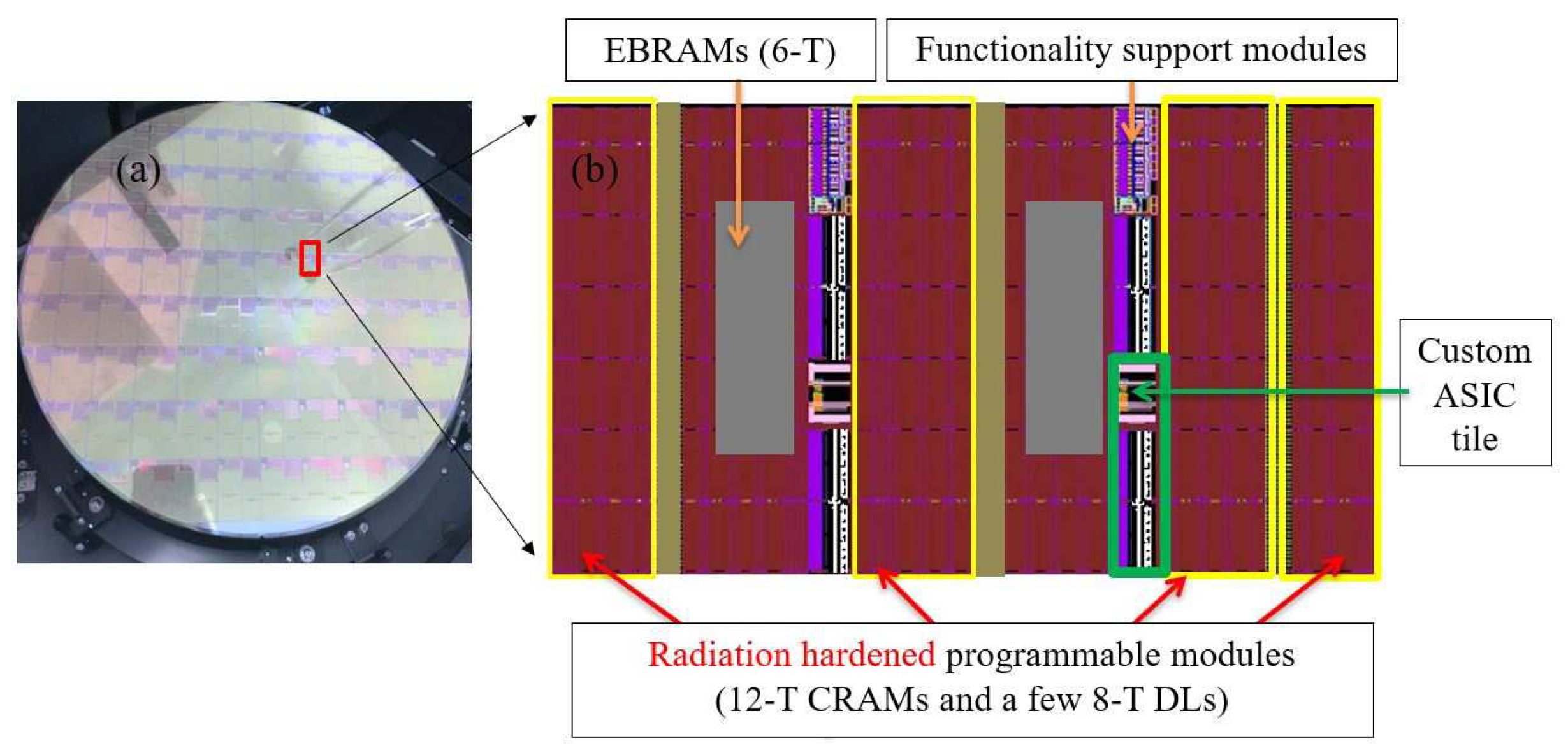
Abstract
1. Introduction
2. DUT Introduction
2.1. DUT Parameters
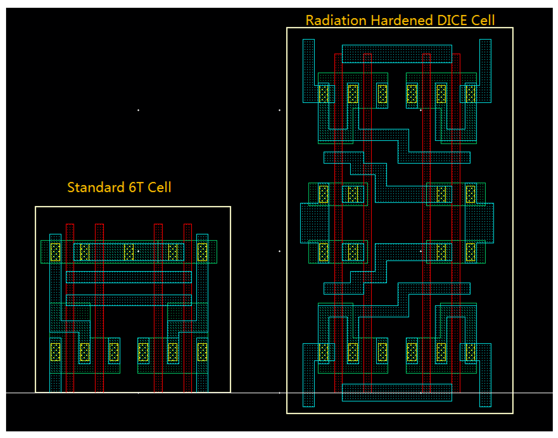
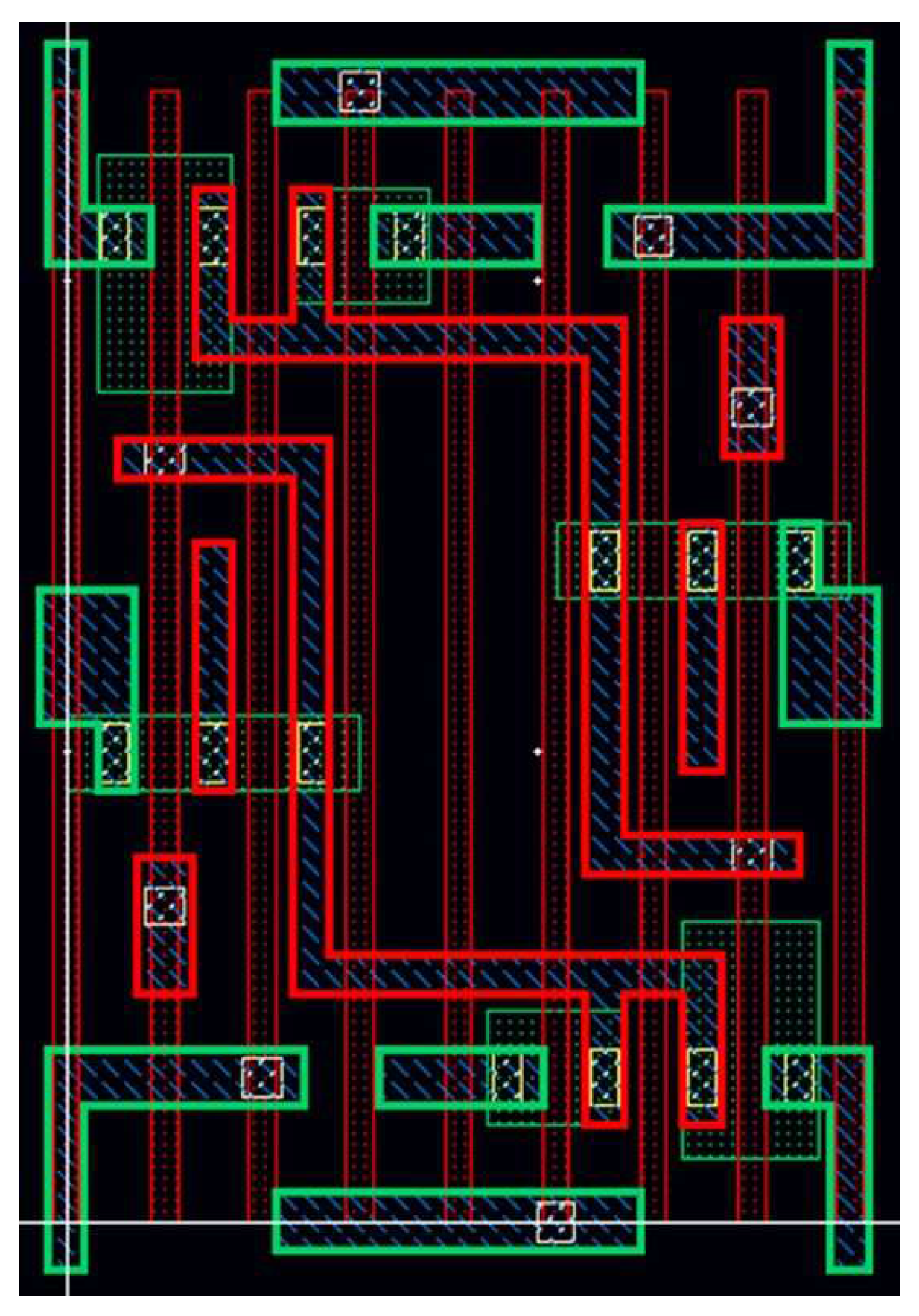
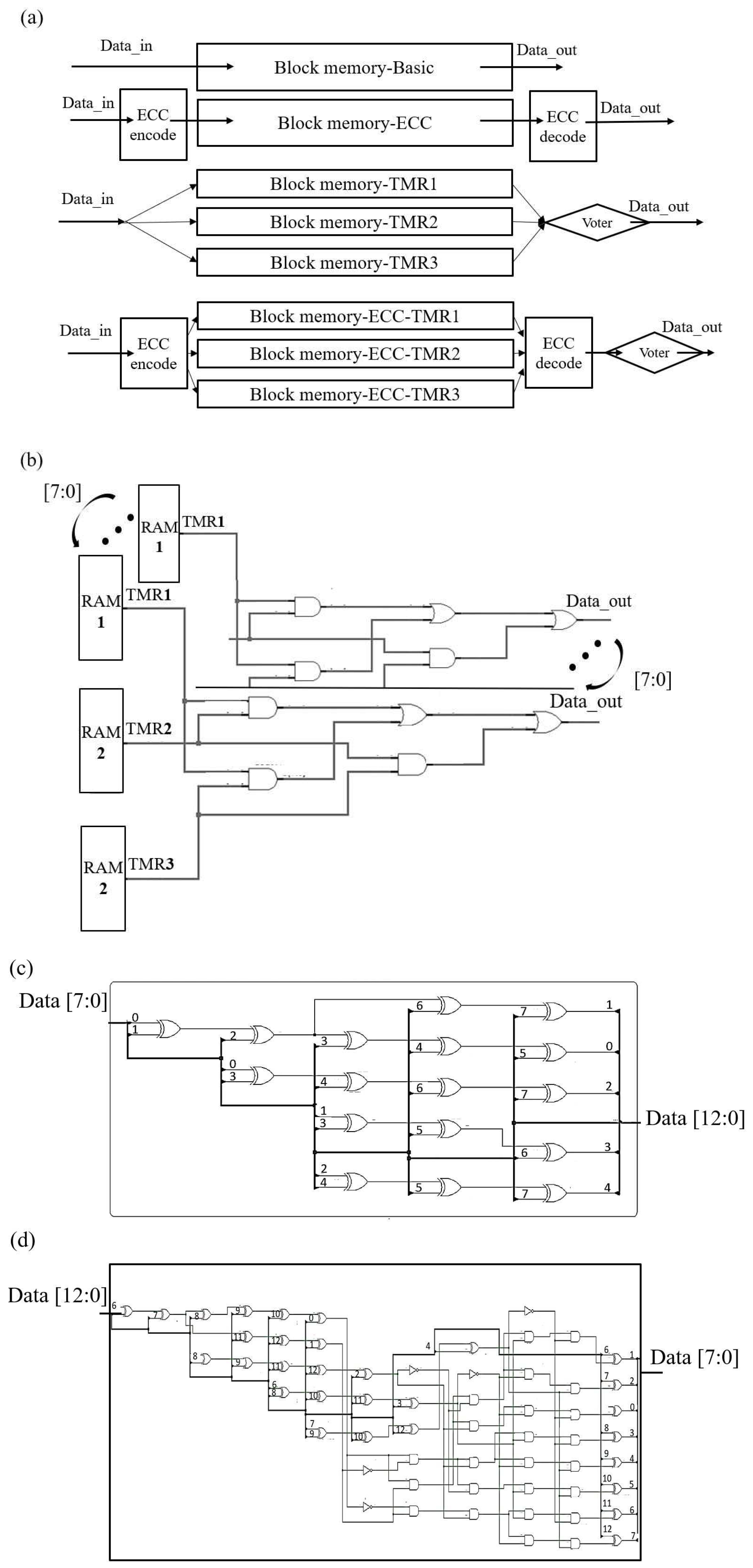
2.2. Radiation Hardening Design
3. Heavy-Ion Test
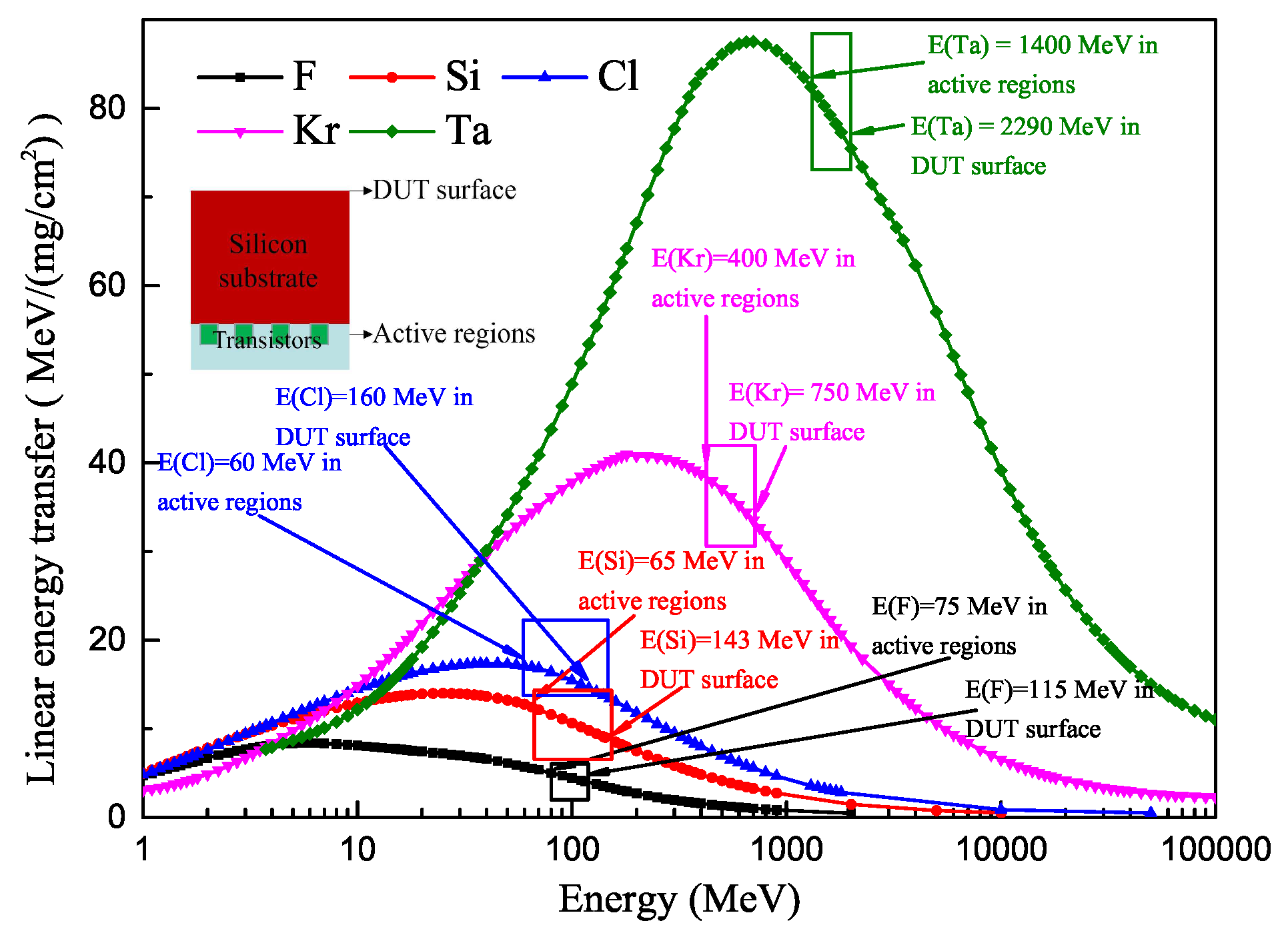
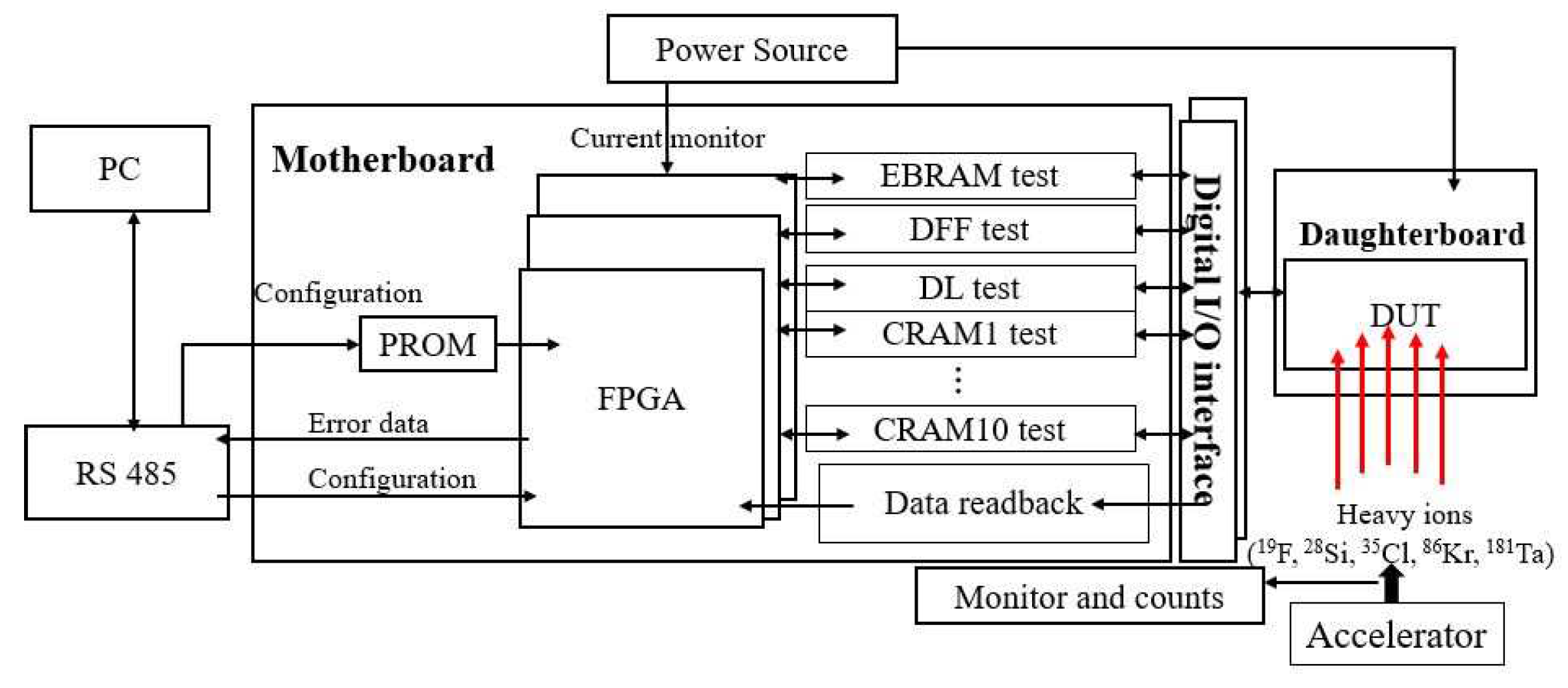
3.1. Experimental Setup
3.2. Experimental Results
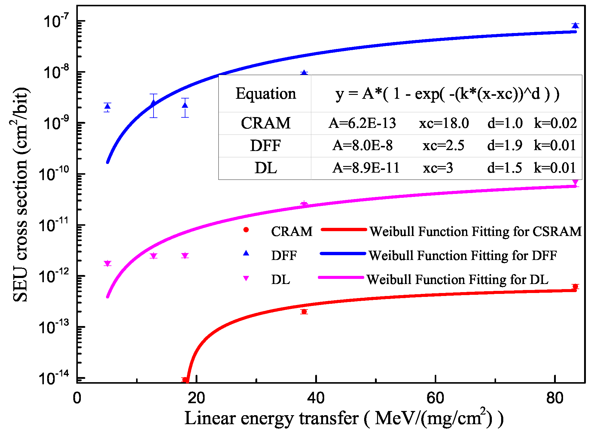
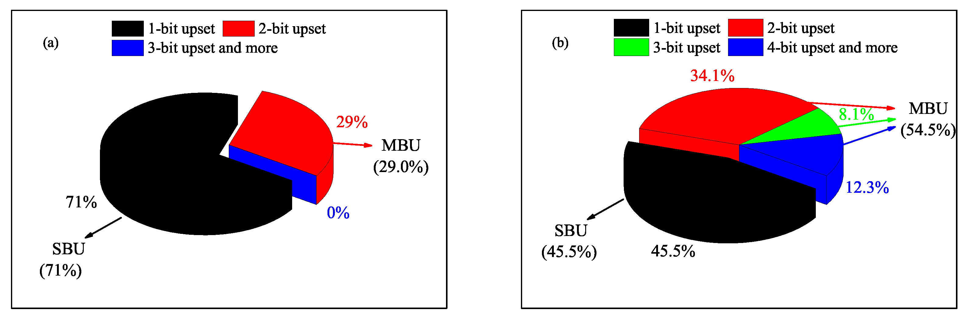
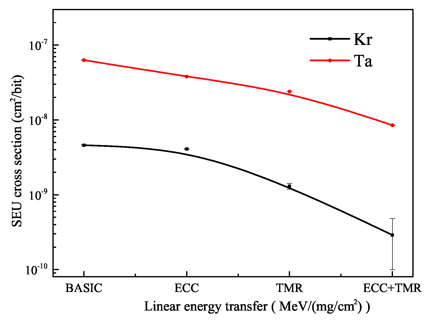
3.2.1. Effectiveness of Layout Hardening
3.2.2. Effectiveness of Configuration Hardening
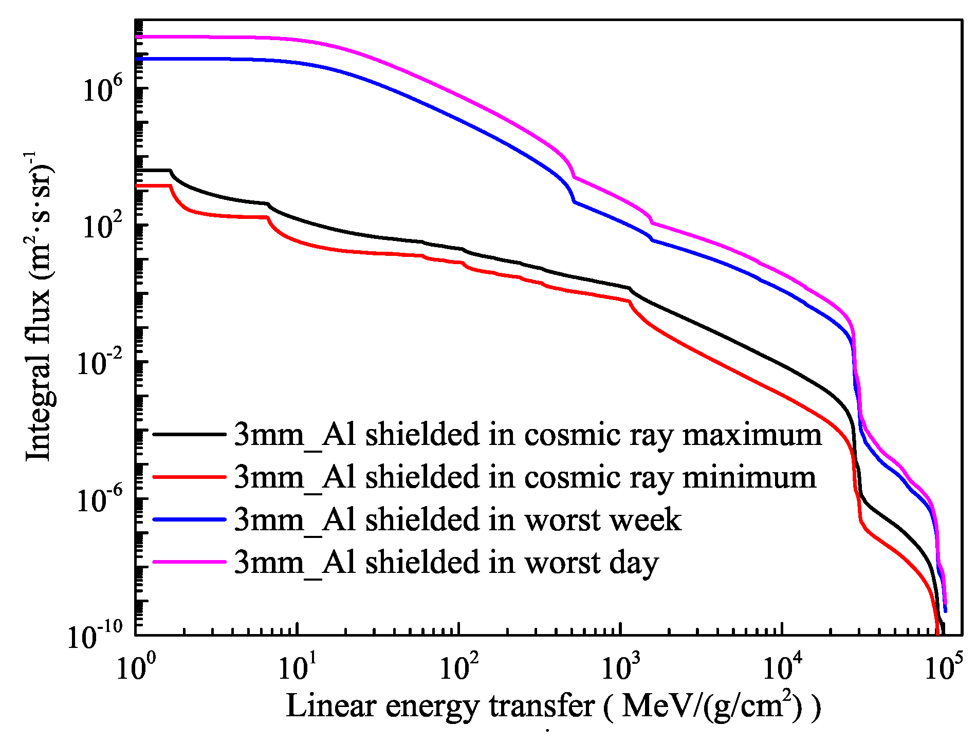
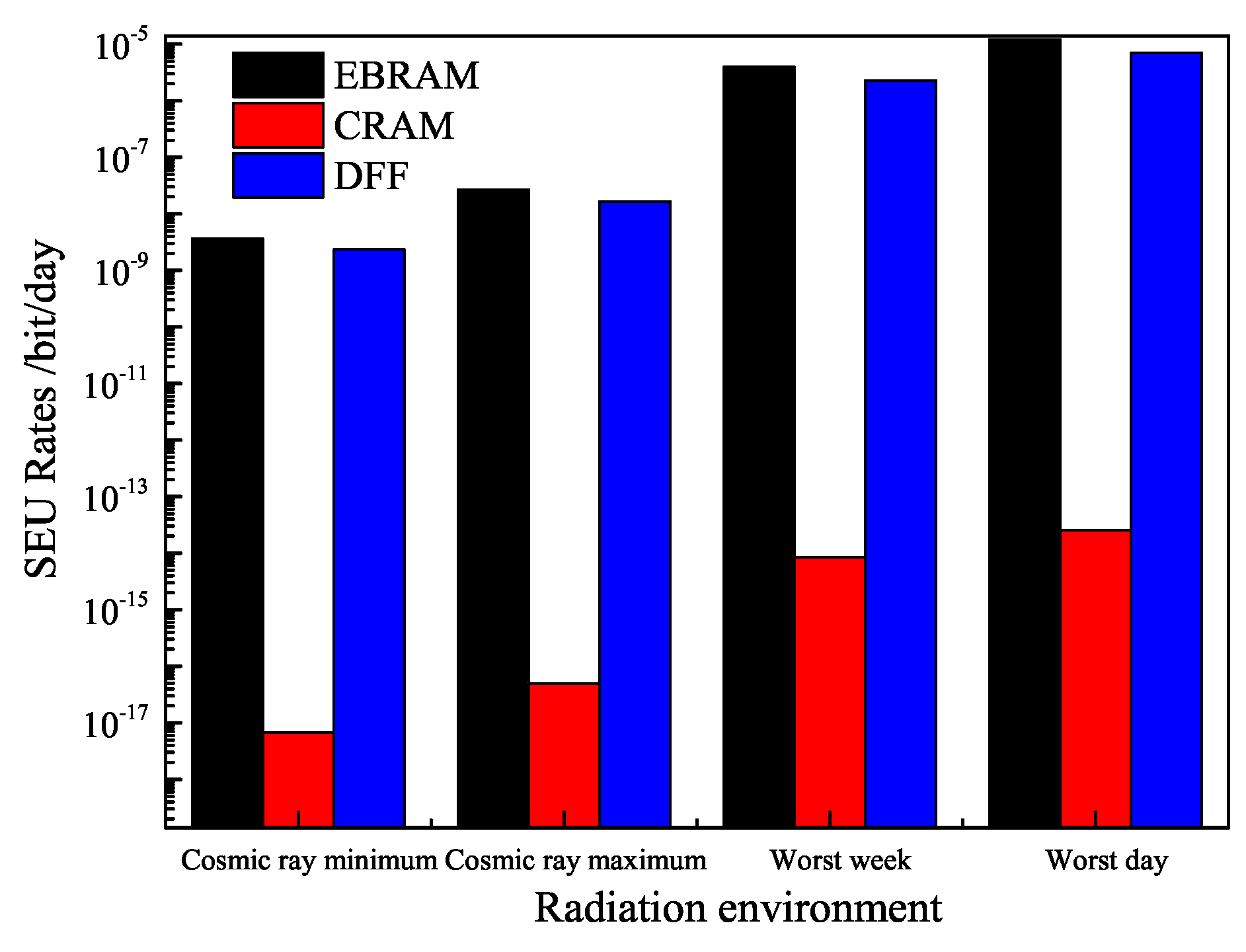
4. SEU Rates Prediction
5. Discussion
5.1. Radiation Hardening Design
5.2. Convincible Prediction and Perspectives
6. Conclusions
Author Contributions
Funding
Acknowledgments
Conflicts of Interest
References
- Rose, J.; ElGamal, A.; Sangiovanni-Vincentelli, A. Architecture of Field-Programmable Gate Arrays. Proc. IEEE 1993, 81, 1013–1029. [Google Scholar] [CrossRef]
- Stroud, C.; Nall, J.; Lashinsky, M.; Abramovici, M. Bist-based diagnosis of fpga interconnect. In Proceedings of the International Test Conference, Baltimore, MD, USA, 8–10 October 2002; pp. 618–627. [Google Scholar] [CrossRef]
- George, J.; Koga, R.; Swift, G.; Allen, G.; Carmichael, C.; Tseng, C.W. Single Event Upsets in Xilinx Virtex-4 FPGA Devices. In Proceedings of the IEEE Radiation Effects Data Workshop (REDW), Ponte Vedra, FL, USA, 17–21 July 2006; pp. 109–114. [Google Scholar] [CrossRef]
- Berg, M.; Poivey, C.; Petrick, D.; Espinosa, D.; Lesea, A.; Label, K.A. Effectiveness of internal versus external SEU scrubbing mitigation strategies in a Xilinx FPGA: Design, test, and analysis. IEEE Trans. Nucl. Sci. 2008, 55, 2259–2266. [Google Scholar] [CrossRef]
- Koga, R.; George, J.; Swift, G.; Yui, C.; Edmonds, L.; Carmichael, C.; Langley, T.; Murray, P.; Lanes, K.; Napier, M. Comparison of Xilinx Virtex-II FPGA SEE sensitivities to protons and heavy ions. IEEE Trans. Nucl. Sci. 2004, 51, 2825–2833. [Google Scholar] [CrossRef]
- Graham, P.; Caffrey, M.; Johnson, D.E.; Rollins, N.; Wirthlin, M. SEU mitigation for half-latches in Xilinx Virtex FPGAs. IEEE Trans. Nucl. Sci. 2003, 50, 2139–2146. [Google Scholar] [CrossRef]
- Gregory, A. Virtex-4QV Static SEU Characterization Summary. In NASA Electronic Parts and Packaging Program Office of Safety and Mission Assurance; National Aeronautics and Space Administration: Washington, DC, USA, 2008; pp. 1–15. [Google Scholar]
- Swift, G.M.; Allen, G.R.; Tseng, C.W.; Carmichael, C.; Miller, G.; George, J.S. Static Upset Characteristics of the 90 nm Virtex-4QV FPGAs. In Proceedings of the IEEE Radiation Effects Data Workshop (REDW), Tucson, AZ, USA, 14–18 July 2008; pp. 98–105. [Google Scholar] [CrossRef]
- Chen, W.; Liu, J.; Ma, X.; Guo, G.; Zhao, Y.; Guo, X.; Luo, Y.; Yao, Z.; Ding, L.; Wang, C.; et al. Research progress of radiation effects mechanisms and experimental techniques in nano-devices. Chin. Sci. Bull. 2018, 63, 1211–1222. [Google Scholar] [CrossRef]
- Liu, T.; Liu, J.; Xi, K.; Zhang, Z.; He, D.; Ye, B.; Yin, Y.; Ji, Q.; Wang, B.; Luo, J.; et al. Heavy Ion Radiation Effects on a 130-nm COTS NVSRAM Under Different Measurement Conditions. IEEE Trans. Nucl. Sci. 2018, 65, 1119–1126. [Google Scholar] [CrossRef]
- Maillard, P.; Hart, M.; Barton, J.; Chang, P.; Welter, M.; Le, R.; Ismail, R.; Crabill, E. Single-event upsets characterization evaluation of Xilinx UltraScale Soft Error Mitigation (SEM IP) Tool. In Proceedings of the IEEE Radiation Effects Data Workshop (REDW), Portland, OR, USA, 11–15 July 2016; pp. 1–4. [Google Scholar] [CrossRef]
- Tonfat, J.; Kastensmidt, F.L.; Artola, L.; Hubert, G.; Medina, N.H.; Added, N.; Aguiar, V.A.P.; Aguirre, F.; Macchione, E.L.A.; Silveira, M.A.G. Analyzing the Influence of the Angles of Incidence and Rotation on MBU Events Induced by Low LET Heavy Ions in a 28-nm SRAM-based FPGA. IEEE Trans. Nucl. Sci. 2017, 64, 2161–2168. [Google Scholar] [CrossRef]
- Andrew, M.K.; Timothy, A.W.; Kenneth, B.S.; Michael, J.W. Dynamic SEU Sensitivity of Designs on Two 28-nm SRAM-Based FPGA Architectures. IEEE Trans. Nucl. Sci. 2018, 65, 280–287. [Google Scholar] [CrossRef]
- Inguimbert, C.; Duzellier, S.; Ecoffet, R.; Guibert, L.; Barak, J.; Chabot, M. Using a carbon beam as a probe to extract the thickness of sensitive volumes. IEEE Trans. Nucl. Sci. 2000, 47, 551–558. [Google Scholar] [CrossRef]
- Hamming, R.W. Error detecting and error correcting codes. Bell Syst. Tech. J. 1950, 29, 147–160. [Google Scholar] [CrossRef]
- Sierawski, B.D.; Mendenhall, M.H.; Weller, R.A.; Reed, R.A.; Adams, J.H.; Watts, J.W.; Barghouty, A.F. CREME-MC: A Physics-Based Single Event Effects Tool. In Proceedings of the IEEE Nuclear Science Symposium and Medical Imaging Conference (NSS/MIC), Knoxville, TN, USA, 30 October–6 November 2010; pp. 1258–1261. [Google Scholar] [CrossRef]
- Weller, R.A.; Mendenhall, M.H.; Reed, R.A.; Schrimpf, R.D.; Warren, K.M.; Sierawski, B.D.; Massengill, L.W. Monte Carlo Simulation of Single Event Effects. IEEE Trans. Nucl. Sci. 2010, 57, 1726–1746. [Google Scholar] [CrossRef]
- Bradford, J. Geometric Analysis of Soft Errors and Oxide Damage Produced by Heavy Cosmic Rays and Alpha Particles. IEEE Trans. Nucl. Sci. 1980, 27, 941–947. [Google Scholar] [CrossRef]
- Mendenhall, M.; Weller, R. A probability-conserving cross-section biasing mechanism for variance reduction in Monte Carlo particle transport calculations. Nucl. Instrum. Methods Phys. Res. A 2011, 667, 38–43. [Google Scholar] [CrossRef]
- Bellato, M.; Bernardi, P.; Bortolato, D.; Candelori, A.; Ceschia, M.; Paccagnella, A.; Rebaudengo, M.; Reorda, M.S.; Violante, M.; Zambolin, P. Evaluating the effects of SEUs affecting the configuration memory of an SRAM-based FPGA. In Proceedings of the Design, Automation and Test in Europe Conference and Exhibition (DATE), Paris, France, 16–20 February 2004; pp. 584–589. [Google Scholar] [CrossRef]
- Gregory, A.; Larry, E.; Chen, W.T.; Gary, S.; Carl, C. Error Detect and Correct Enabled Block Random Access Memory (Block RAM) Within the Xilinx XQR5VFX130. IEEE Trans. Nucl. Sci. 2010, 57, 3426–3431. [Google Scholar] [CrossRef]
- Lei, Z.; Zhang, Z.; En, Y.; Huang, Y. Mechanisms of atmospheric neutron-induced single event upsets in nanometric soi and bulk sram devices based on experiment-verified simulation tool. Chin. Phys. B 2018, 27, 066105. [Google Scholar] [CrossRef]


© 2019 by the authors. Licensee MDPI, Basel, Switzerland. This article is an open access article distributed under the terms and conditions of the Creative Commons Attribution (CC BY) license (http://creativecommons.org/licenses/by/4.0/).
Share and Cite
Cai, C.; Fan, X.; Liu, J.; Li, D.; Liu, T.; Ke, L.; Zhao, P.; He, Z. Heavy-Ion Induced Single Event Upsets in Advanced 65 nm Radiation Hardened FPGAs. Electronics 2019, 8, 323. https://doi.org/10.3390/electronics8030323
Cai C, Fan X, Liu J, Li D, Liu T, Ke L, Zhao P, He Z. Heavy-Ion Induced Single Event Upsets in Advanced 65 nm Radiation Hardened FPGAs. Electronics. 2019; 8(3):323. https://doi.org/10.3390/electronics8030323
Chicago/Turabian StyleCai, Chang, Xue Fan, Jie Liu, Dongqing Li, Tianqi Liu, Lingyun Ke, Peixiong Zhao, and Ze He. 2019. "Heavy-Ion Induced Single Event Upsets in Advanced 65 nm Radiation Hardened FPGAs" Electronics 8, no. 3: 323. https://doi.org/10.3390/electronics8030323
APA StyleCai, C., Fan, X., Liu, J., Li, D., Liu, T., Ke, L., Zhao, P., & He, Z. (2019). Heavy-Ion Induced Single Event Upsets in Advanced 65 nm Radiation Hardened FPGAs. Electronics, 8(3), 323. https://doi.org/10.3390/electronics8030323