Abstract
Integration of rooftop solar-PV (RTSPV) systems and extensive use of nonlinear loads in the low-voltage distribution system (LVDS) leads to poor power quality (PQ). Therefore, it is necessary to address the issues leading to poor PQ at the point of common coupling of the LVDS. In this article, a multi-band hysteresis current control (MB-HCC) for the multi-functional inverter (MFI) is proposed which improves the efficiency of the MFI and also enhances the PQ of the LVDS. The MB-HCC uses simple switching logic and outperforms in its multi-functional tasks such as active power injection and power conditioning. MB-HCC offers better efficiency over variable double-band HCC (VDB-HCC) as it operates at a lower switching frequency. The performance of the proposed system is simulated by using MATLAB/Simulink and validated by OPAL-RT based real-time simulation studies. During the variation of solar irradiation, the proposed MFI has an average efficiency of 98.5% under the ideal grid and 97.34% under the distorted grid. Moreover, the percentage of Total Harmonic Distortion under ideal and distorted grid conditions is brought down to below 5%, and also, reactive power compensation maintains unity power factor operation complying with the IEEE-519-2014 and 1547 standards. These results substantiate the hypothesis of scalability of the single-phase MB-HCC-based MFI for an LVDS contributing to economy and ecology.
1. Introduction
The number of installations of rooftop solar-PV (RTSPV) systems in low-voltage distribution systems (LVDS) is growing. Such a high penetration is due to the rise of consumer demand associated with high electricity tariffs furthering deterioration of environmental concerns [1,2]. The availability of low-cost SPV panels and advanced power electronic converters made RTSPV feasible and viable, reducing the dependency on conventional energy resources [3,4]. Moreover, government policies are encouraging consumers to install the RTSPV systems and become prosumers to receive payback for the energy supplied to the grid through net metering which reduces consumption of grid power [4,5].
While the growth of grid-connected RTSPV systems is welcome, the poor power quality (PQ) introduced by power electronic converters is not worthy. The other reason for the deterioration of PQ in LVDS is power electronic-based nonlinear loads such as air conditioners, arc welding machines, compact fluorescent lamps, consumer electronics, light emitting diode lamps, personal computers, uninterruptible power supplies, and electric vehicle charging stations [6,7,8,9]. The poor PQ affects the performance of appliances in a single-phase LVDS due to current harmonic distortion and induced reactive power causing overheating of the equipment, machine vibration, blowing of capacitor fuses, imprecise metering, and malfunctioning of protection systems [9]. This will influence the stability and the reliability of LVDS, impacting the national economy negatively.
A two-stage RTSPV integration is an efficient system for single-phase rooftop installations which perform both active power feeding and power conditioning at the point of common coupling (PCC) to the LVDS in tune with the global standards. This approach helps us avoid the use of power conditioning equipment [10,11,12,13,14,15]. A two-stage RTSPV integration system consists of a DC-DC boost stage and multi-functional inverter (MFI) stage. Literature survey suggests that the selection of an efficient maximum power point tracking (MPPT) technique for the DC-DC boost stage, designing of a simple control methodology for the inverter to coordinate the multi-functional operations such as grid synchronization with active power feeding, reactive power, and harmonic compensation are still major topics to be explored under both ideal and distorted grid conditions. However, designing simple control for single-phase multi-functional system is not addressed sufficiently in the literature [15].
Several MPPT techniques have been reported in the literature [15,16,17,18]. MFI perturb and observe (P&O) technique applications have been adopted for maximum power extraction [15,16]. Incremental conductance (INC)-based MPPT is also another technique for maximum power extraction. The advantages of INC-based MPPT over P&O-based MPPT are: (i) No need to compute power, (ii) better dynamic response, and (iii) low ripple power. Given the simplicity, efficiency, accuracy, and tracking capabilities of the INC-based MPPT technique for the DC-DC boost stage, converters are exploited in this research work.
The control technique is very crucial to improve the robustness and efficiency of an MFI. Various current control techniques are reported in the literature, with their own merits and demerits, depending on the system operating conditions [10]. Cupertino et al. proposed a proportional–integral (PI) current control method [19] to perform the multi-functional operations using a grid-connected SPV inverter. However, tuning the gain values of the PI controller as per the variations in solar irradiation and consumer loads is quite complicated. The proportional–resonant (PR) controller has been proposed for better dynamics over the PI controller [20], but the PR controller is a complex controller and selection of the individual harmonic frequency for compensation under distorted grid conditions is one of the limitations. Chatterjee et al. reported that the model predictive controller-based PV inverter integrated with the grid [21]. Nevertheless, the requirement of the high sampling frequency, i.e., 200 kHz, and the optimization process agnostic to the controller cost function and heavy computation during the operation of single-phase systems affected nonlinear loads. Kim proposed sliding mode control for grid-connected SPV systems. However, the time-varying surface selection is a complex task to perform multifunctional operations [22].
In contrast to the above methods, the hysteresis current control (HCC) is a simple method for multi-functional operation as it offers advantages such as rapid current controllability, easy implementation, and load insensitivity with respect to parameter variations, maximum current limit, and better stability [15,16,23,24,25,26,27,28]. But, the major limitation of the HCC is its highly variable switching frequency to match variation in solar irradiation and associated compensation requirements that results in higher switching losses. To overcome the drawback of high variable switching frequency, advanced HCC methods are described in the literature [29,30,31]. A variable double-band (VDB)-HCC concept is presented in [30] for single-phase full-bridge bi-directional converters. However, the selection of the optimum variable hysteresis band to attain the highest efficiency is not yet reported.
Moreover, the double-band (DB)-HCC concept for single-phase active filtering is presented in References [29,31]. The bandwidth of the DB-HCC method proposed in References [29,31] is constant, and the compensation objective depends on the bandwidth values. Moreover, there is an offset issue under distorted grid condition which has a limitation in compensation with varying highly distorted nonlinear load conditions under a weak grid. The detailed comparison of the HCC methods, in view of the performance under weak grid (PWG), active power injection (API), PQ improvement (PQI), steady-state and transient characteristics (SS & TC), inverter peak efficiency (IPE), inverter efficiency under low irradiation (IELI), average switching frequency (ASF), and implementation complexity (IC) are exhibited in Table 1.

Table 1.
Comparison of previous hysteresis current control (HCC)-based single-phase grid-tied inverter literature.
Table 1 shows the metrics for single-phase grid-tied inverters, where the HCC method shows a limitation related to the highly variable switching frequency leading to switching losses and hence reduction in the MFI conversion efficiency. On the other hand, the VDB-HCC-based bi-directional converter [30] and the DB-HCC-based active power filter configuration [31] have not been explored for weak-grid conditions; also, the IELI is not reported. Particularly, the DB-HCC [29,31] exhibits unipolar switching characteristics to reduce the switching losses, but during the zero modulation index case, it has a limitation of high switching frequency. Moreover, the inverter switches are triggered with imbalance switching pulses. In addition to that, the inverter multi-functional capabilities are not explored using DB-HCC. The VDB-HCC method is an alternative method to overcome the limitations of the DB-HCC method, however, the selection of the optimum variable band to attain maximum efficiency is not yet reported. Moreover, VDB-HCC is also not considered for MFI operation. Hence, it is necessary to explore the DB-HCC method application concerning the fast, reliable, and efficient operation of the MFI to perform multifunctional tasks effectively and also to overcome the limitations of the VDB-HCC method for MFI operation. The selection of the appropriate MPPT for boost converter is also important, to extract the maximum power from RTSPV under variable environmental conditions in order to support the multi-functional capabilities of MFI. Further, it is also necessary to consider the effect of the distorted grid condition while designing the control method for MFI as per IEEE 519-2014 [32]. To fulfill the aforementioned tasks, in this paper the authors propose a scaling factor-based multi-band (MB)-HCC with a simple switching logic by employing the two hysteresis bands with reduced switching frequency to reduce switching losses in the inverter and thereby increasing the inverter efficiency. Proposed MB-HCC bandwidths are adjusted as per the current reference value using scaling factors under ideal and distorted grid conditions. In the proposed MB-HCC-based two-stage RTSPV system, the DC-DC boost converter stage is controlled with the INC-based MPPT to extract the maximum power from RTSPV, and the MFI stage is tuned with the proposed MB-HCC, with scaling factors to execute the multifunctional operations to reduce the grid consumption and improve the PQ of the LVDS. The proposed system configuration is modeled and simulated in a MATLAB/Simulink environment using sim power system toolbox. The simulated results are validated in real-time (RT) using an RT grid simulator.
The main contributions of this article are as follows:
- Proposed scaling factor-based MB-HCC was proposed to MFI for power injection and power conditioning operations.
- Verified the proposed MB-HCC MFI operation under both ideal and distorted grid conditions using simulation and RT experimental studies.
- Compared the proposed MB-HCC method effectiveness with the VDB-HCC method reported in Reference [30].
The organization of the paper is as follows: The proposed RTSPV integration system is presented in Section 2 followed by a control methodology in Section 3. The simulation and RT results are presented in Section 4 and Section 5. The results discussion is described in Section 6, and, finally, conclusions are presented in Section 7.
2. Configuration of RTSPV Integration System for LVDS Applications
In this section, the detailed schematic of the RTSPV integration system configuration for LVDS applications is illustrated in Figure 1. The RTSPV system is connected in parallel to the LVDS at the point of common coupling (PCC). The single-phase system is modeled as an ideal AC voltage source in series with the source impedance, and it is connected to the nonlinear loads as depicted in Figure 1. The key building blocks of the RTSPV system are the two-stage power circuit and the MB-HCC architecture. The two-stage power circuit consists of an INC-based MPPT-controlled DC-DC boost converter coupled with a current controlled voltage source inverter (VSI) as MFI with RTSPV interfacing.
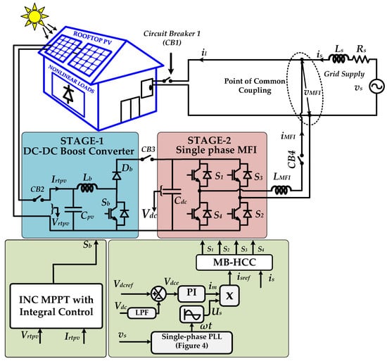
Figure 1.
Proposed multi-band (MB)-HCC-based two-stage multi-functional inverter (MFI) for single-phase low voltage distribution systems (LVDS).
2.1. RTSPV System Modeling
A single diode model is considered as a PV cell for building the PV array in simulation studies [33]. According to the single diode model, the RTSPV output current and power are expressed as follows:
In this work, the RTSPV array is designed to deliver a maximum power of 6 kWp with 1000 W/m2 solar irradiation at 25 °C temperature conditions.
The shade-free rooftop space required for the SPV installation is considered as 732 sq.ft as per the design procedures [5]. While building the SPV array using a MATLAB/Simulink environment, five series and four parallel SUN POWER SPR-305 WHT PV [34] modules were considered to build the PV array, which is capable of generating the 6.1 kWp power using MPPT-controlled DC-DC boost converter. The Irtpv-Vrtpv and Prtpv-Vrtpv characteristics of the RTSPV array concerning the variation of solar irradiation are depicted in Figure 2.
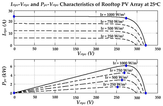
Figure 2.
Irtpv-Vrtpv and Prtpv-Vrtpv characteristics of rooftop solar-PV (RTSPV) array.
2.2. DC-DC Boost Converter Stage with MPPT Control
The RTSPV is connected to a DC-DC boost converter to supply the regulated DC-link voltage to the inverter. Here the DC-link voltage of the MFI is rated at 500 V. The boost stage DC-DC converter will amplify the RTSPV array voltage to rated DC-link voltage; simultaneously, it will inject the PV power. The duty cycle (D) of the MPPT algorithm for boost operation is computed by using the following expressions:
The duty cycle to trigger the boost converter for boost operation is calculated according to the INC MPPT algorithm to maintain the set value of MFI DC-link voltage. The MPPT control is depicted in Figure 1. Due to the intermittent nature of solar energy and the availability of a shade-free rooftop area of the building, the boost stage with MPPT is essential for a single-phase system to extract the maximum power from RTSPV.
2.3. Muti-Functional Inverter Design
A single-phase four-switch H-bridge VSI is considered as MFI to execute the active power injection and power conditioning operations. The inverter is connected to the PCC by a ripple filter (LMFI) as shown in Figure 1. Here the source current (is) is sensed and compared with the reference current (isref) generated by the sine-based unit vector template approach, then processed through the proposed MB-HCC method to perform the multifunctional operation with reduced switching frequency. The system parameters used in this study are tabulated in Table 2. The detailed control configuration is presented in the next section.
Table 2.
System parameters.
3. Multi-Functional Inverter Control Configuration
The objective of the controller was to pump the harvested maximum power from RTSPV to the PCC of the LVDS through the MFI and PQ enhancement at PCC. The active power generated from the MFI is expressed as follows
where Plosses constitutes the majority of switching losses of the MFI. The efficiency of the MFI can be improved by minimizing the switching losses. While converting the RTSPV DC power to the AC power using MFI, there will be some amount of losses, but if the losses are reduced by minimizing the inverter switching losses, then the efficiency of the MFI is improved. Hence, the MB-HCC switching logic was designed to reduce the switching losses, thereby improving the MFI efficiency. The MFI controller configuration had two control loops—one was for inverter DC-link voltage control, and the other one was for current control.
3.1. Reference Current Generation Scheme for MFI Control and Grid Synchronization
The detailed block diagram of the RTSPV interfaced MFI control is illustrated in Figure 1. The sensed DC-link voltage supplied from the DC-DC boost stage was processed by a low-pass filter (LPF) to reduce the DC-link voltage ripples compared with its reference DC-link voltage value. To regulate the DC-link voltage, the error voltage was processed through the proportional–integral (PI) voltage controller. The DC-link voltage error (Vdce) sample value at nth point is expressed as
This output of the PI voltage controller is the peak value of the source current. The output expression of the discrete PI voltage controller is represented as
where the kp and ki gain values are obtained by using the Ziegler-Nichols second method [35,36]. Initially, the kp gain value was set by the Ziegler–Nichols second method table value as 0.6, then the tuning procedure was continued by the proportional-integral-derivative (PID) controller autotuning in the MATLAB/Simulink environment to obtain the ki value for improved performance. After successful tuning using the PID auto-tuning procedure in the MATLAB/Simulink environment, the ki gain value was obtained as 10. The main objective of this tuning is for attaining the lowest percentage total harmonic distortion (THD) of the grid current which is within the limits of IEEE 519-2014 and IEEE 1547 standards, respectively [11,32]. The PI controller gains of the DC-link voltage loop were tuned for a low crossover of the frequency range, i.e., in between 10 Hz to 20 Hz, to attenuate the high-magnitude ripple content in MFI DC-link voltage. The Bode plot of the tuned PI controller with the obtained gain values of the MFI DC-link voltage control loop which regulated the DC-link voltage and reduced the steady-state error is depicted in Figure 3.
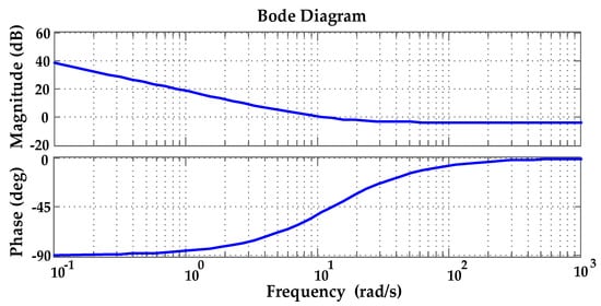
Figure 3.
Bode plot of the MFI DC-link voltage proportional–integral (PI) controller.
The unit vector (Us) is generated by using the grid synchronizing angle (), which is obtained from a phase-locked loop (PLL) [37,38,39]. The PLL used in the MFI control under both ideal and distorted grid conditions is illustrated in Figure 4. The PLL parameters selected in the MATLAB/Simulink 2013 environment for both simulation and RT implementation are tabulated in Table 3. The main objective of this PLL was to obtain the synchronization angle accurately under ideal and distorted grid conditions, in order to generate the sine unit vector template (Us). The peak value of the source current (im) was multiplied by the Us to generate the source current reference (isref) in phase with source voltage at unity power factor. To purge the harmonics and reactive power under ideal and distorted grid conditions, it was necessary to force the source current to maintain a sinusoidal nature, and it should be in phase with the source voltage. The sine unit vector template and reference source current expressions under ideal and distorted grid conditions are given as follows:
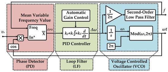
Figure 4.
Single-phase phase-locked loop (PLL) used for both ideal and distorted grid voltage cases.
Table 3.
PLL parameters.
The reference current is compared with the actual current to initiate the switching of the inverter. The design of the MB-HCC control methodology is discussed in the next section.
3.2. Current Control Methodology
In this section, the VDB-HCC and the proposed MB-HCC methods are described.
3.2.1. VDB-HCC
In the VDB-HCC, the switching logic was derived by considering the two hysteresis bands (HBs), where the HBs bandwidths were comprised of a minimum band value and a maximum band value. Here, the maximum band was multiplied by one fundamental periodic cycle [30].
The switching logic of the VDB-HCC method used in Reference [30] is illustrated as given below:
where, the HB is expressed as follows
| VDB-HCC Switching Logic for MFI |
|
By considering the average hysteresis band expression, various combinations are derived as listed in Reference [30]. Among the various combinations of maximum and minimum hysteresis bandwidth values, hmin = 0.005 and H = 0.149226 are selected in view of the better performance indices as reported in Reference [30]. The main limitation of the VDB-HCC is the high variable switching frequency during the variations in solar irradiation and nonlinear load compensation requirements. The inverter switches Turned ON and OFF for a long time during the source current touched the maximum hysteresis band as shown in Figure 5a. Moreover, efficiency was low for the modulation index value of less than 0.7 [30]. The mathematical expression for switching frequency (fsw) of the single-phase inverter using VDB-HCC described in Reference [30] is expressed as
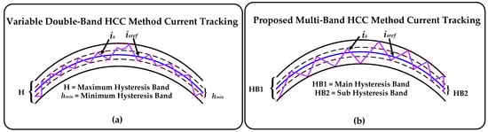
Figure 5.
Comparision of the variable double-band (VDB)-HCC method and the proposed MB-HCC method current tracking; (a) VDB-HCC current tracking; (b) MB-HCC current tracking.
Here, DC-link voltage (Vdc) and ripple inductor (LMFI) values are fixed values. Hence, the switching frequency can be controlled by varying the hysteresis bandwidths as represented in Equation (11). The reported bandwidth values are not optimum for the multifunctional operation of the inverter. Moreover, the optimum bandwidths of the hysteresis bands to attain high efficiency are not yet reported. To overcome the aforementioned limitations and also to achieve low average switching frequency, an MB-HCC method is proposed in this paper and is described in the next subsection.
3.2.2. Proposed MB-HCC
In this proposed MB-HCC method, two hysteresis bands are derived based on the scaling factors approach. This method controls the MFI switches in such a way that it can force the actual source current (is) to rise and fall and closely tracks reference current (isref) between the main and sub hysteresis bands (HB1 and HB2) as depicted in Figure 5b. The detailed flowchart of the MB-HCC algorithm is illustrated in Figure 6. The switching pulses are generated through tracking current response between dual hysteresis bands (HB1 and HB2). In contrast to the VDB-HCC method, the MB-HCC method balances the switching frequency based on the current tracking uniformly, as shown in Figure 5b.
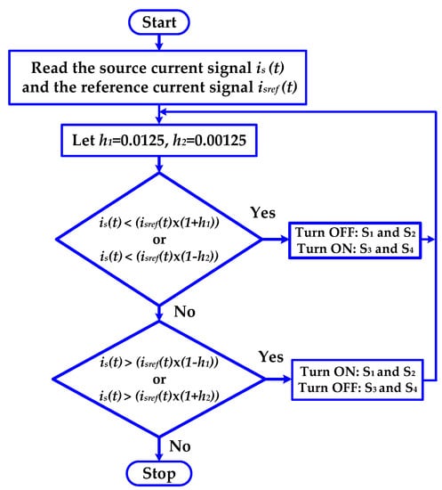
Figure 6.
Detailed representation of the stage-2 MB-HCC algorithm.
The h1 and h2 are the scaling factors of the dual hysteresis bands (HB1 and HB2) of the MB-HCC. The optimum values of the scaling factors were set and verified by the RT simulation studies to obtain the reduced THD as well as the MFI switching frequency simultaneously.
The scaling factors are obtained by the following step by step procedure.
| Step-by-step procedure for MB-HCC scaling factor selection | |
| Step 1: | Initially, the hysteresis band scaling factor (h1) range is obtained as 0.01 to 0.1 by using the generalized instantaneous switching frequency formula reported in Reference [40] to get the lowest % THD at the reduced switching frequency (fsw). |
| Step 2: | The scaling factor (h2) is considered as 10% of the h1 to prevent the offset issues. |
| Step 3: | MATLAB and RT simulations are performed for the range of scaling factors 0.01 to 0.1 in order to obtain the optimum scaling factors for accurate tracking of the actual source current (is). |
| Step 4: | Based on the series of simulation studies with nonlinear loads, the current tracking is accurate with the scaling factor values of h1 = 0.0125 and h2 = 0.00125 (i.e., 10% of h1). Moreover, the % THD low and the average instantaneous switching frequency is nearly constant by considering these scaling factors in MB-HCC method for different nonlinear loads under ideal and distorted grid conditions. |
In the MB-HCC method, the ranges of the two hysteresis bands are adjusted based on the reference current (isref) and their scaling factors (h1 and h2), whereas in the VDB-HCC method, the hysteresis band is determined by using Equation (11). The simple switching logic of the MB-HCC method is as follows:
| MB-HCC Switching Logic for MFI |
|
Unlike the VDB-HCC, in the MB-HCC method, the hysteresis bandwidths are determined by using the reference current and scaling factors as illustrated in Figure 6 in order to determine the optimum bandwidths for improved efficiency and power quality. The MFI switches are triggered by the switching pulses as per the sequence illustrated in Figure 6. These switching pulses generate a pulse width modulated (PWM) AC voltage at the MFI output side (vMFI). This voltage causes a current (iMFI) to flow through the ripple inductor (LMFI), which is injected at PCC to reduce the grid consumption and mitigate the current harmonics and induced reactive power.
4. Simulation Study and Results
A set of simulations on the proposed MB-HCC-based RTSPV integration system configuration was carried out using the MATLAB/Simulink software environment to validate the multi-functionalities under ideal and distorted grid voltage conditions. The voltage was considered as the third- and seventh-order harmonic distorted voltage, in accordance with the limits of IEEE 519-2014 standard [32], i.e., the voltage percentage THD is 8%. The nonlinear loads connected to the LVDS were modeled using a frontend diode bridge rectifier fed with RL and RC elements. The system parameters specified in Table 2 were used in the simulation studies. The performance of the RTSPV interfaced MFI was demonstrated in four modes, under both ideal and distorted grids, which were classified as follows:
- Mode 1: MFI is OFF, and there is no power injection and power conditioning.
- Mode 2: MFI is ON, with grid sharing or power conditioning.
- Mode 3: MFI is ON, with grid feeding and power conditioning.
- Mode 4: MFI is ON, with grid sharing and power conditioning during irradiation change.
4.1. Mode 1: MFI OFF, with No Power Injection or Power Conditioning
Initially, the load behavior at PCC under MFI OFF condition was assessed by simulation studies, and the simulation results illustrate the source current harmonic distortion and reactive power effect under ideal and distorted grid conditions as depicted in Figure 7.
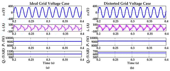
Figure 7.
Simulated waveforms under MFI OFF mode; (a) ideal grid source voltage, current, active, and reactive power; (b) distorted grid source voltage, current, active, and reactive power.
4.1.1. Ideal Grid Voltage Case
Under ideal grid conditions, the source current had a THD percentage of 34.08%. The active and reactive power profiles at PCC under ideal grid conditions is depicted in Figure 7a. The loads draw an active power of 9.068 kW from the grid under the ideal grid condition as shown in Figure 7a. The reactive power under the ideal grid case was 1.005 kVAR.
4.1.2. Distorted Grid Voltage Case
The percentage of THD of the source current under a distorted grid condition was 42.69%. The active and reactive power profiles at PCC under the distorted grid condition is depicted in Figure 7b. The active power consumed from the grid under a distorted grid condition was 9.331 kW as described in Figure 7b. The reactive power under a distorted grid case was 0.655 kVAR. In both cases, the harmonics and reactive power were deteriorating the LVDS power quality. Therefore, it is necessary to compensate for the harmonics and reactive power to improve the operating efficiency and reliability of the LVDS under both ideal and distorted grid conditions.
4.2. Mode 2: MFI is ON, with Grid Sharing and Power Conditioning
In this mode of operation, the MFI functionality as active power injector—to reduce the grid consumption by sharing the RTSPV power and power conditioner to compensate the harmonics and reactive power at PCC—are exhibited under both ideal and distorted grid cases.
4.2.1. Ideal Grid Voltage Case
The source voltage and current responses after compensation of harmonics and reactive power under the ideal grid condition are depicted in Figure 8a along with MFI and load currents. From these results, it is observed that the source current harmonics were compensated, and it was in-phase with the source voltage. Thus, the power conditioning task is achieved effectively. Moreover, grid consumption was also minimized simultaneously. The detailed response of RTSPV power generation at irradiation of 1000 W/m2 and the DC-link voltage responses are presented in Figure 8b. These results confirm that the DC-link voltage is maintained stably at a rated value of 500 V. The load active and reactive power profiles are also illustrated in Figure 8b. The grid sharing response is depicted in Figure 8c; from this, the source power consumption was reduced, which was owing to the active power feeding from the MFI. The MFI also supplied the necessary reactive power to reduce the source side reactive power close to zero, as shown in Figure 8c.
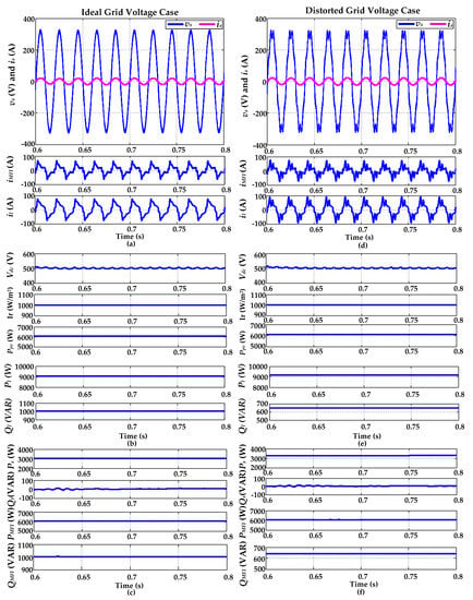
Figure 8.
Simulated output waveforms under MFI ON, grid sharing, and power conditioning mode. (a) Ideal grid input voltage, current, MFI current, and load current; (b) MFI DC-link voltage, solar irradiation, PV power, and load active and reactive power under ideal grid; (c) source active power, reactive power, and MFI active and reactive power under ideal grid; (d) distorted grid input voltage, current, MFI current, and load current; (e) MFI DC-link voltage, solar irradiation, PV power load, and active and reactive power under distorted grid; (f) source active power, reactive power, and MFI active and reactive power under distorted grid.
4.2.2. Distorted Grid Voltage Case
In Figure 8d the source voltage and current responses after compensation of harmonics and reactive power, under the distorted grid voltage condition, are represented along with MFI and load currents. Here, the source current was transformed to sinusoidal and in-phase with the source voltage, irrespective of the load current nature, with the help of the MFI current. The inverter DC-link and RTSPV generation at an irradiation level of 1000 W/m2 is depicted in Figure 8e, where the DC-link was stable at 500 V, and the RTSPV power was 6 kW. In addition to that, the load active and reactive power profiles under distorted grid conditions are also illustrated in Figure 8e. The source reactive power was also reduced close to zero by injecting the required reactive power, as shown in Figure 8f.
Based on the listed active and reactive power summary of the source, load, and MFI under both ideal and distorted grid voltage conditions in Table 4, the MFI performed the grid sharing and power conditioning tasks effectively.
Table 4.
Active and reactive power summary of the source, MFI, and load under grid sharing mode.
4.3. Mode 3: MFI is ON, with Grid Feeding and Power Conditioning
In this mode, the grid feeding and power conditioning operations of the MFI during the reduced load condition under both ideal and distorted grid situations are demonstrated.
4.3.1. Ideal Grid Voltage Case
The source voltage and current responses under grid feeding and power conditioning mode are illustrated in Figure 9a. Here the source current is out of phase with the source voltage, which means that the surplus current, after injecting to the local loads at PCC, is feeding to the grid; the reduced load current nature due to the reduction of the loads is illustrated in Figure 9a. Here, the MFI was serving the local load simultaneously, pumping the excess power to the grid. The inverter DC-link voltage response and the active and reactive power profiles of the loads are presented in Figure 9b. The active and reactive power supplied by the MFI is depicted in Figure 9c.
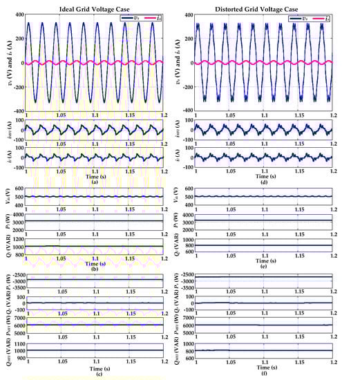
Figure 9.
Simulated output waveforms under MFI ON with grid feeding and power conditioning mode; (a) ideal grid input voltage, current, MFI current, and load current; (b) MFI DC-link voltage, and load active and reactive power under ideal grid; (c) source active power, reactive power, and MFI active and reactive power under ideal grid; (d) distorted grid input voltage, current, MFI current, and load current; (e) MFI DC-link voltage, and load active and reactive power under distorted grid; (f) source active power, reactive power, and MFI active and reactive power under distorted grid.
4.3.2. Distorted Grid Voltage Case
The simulation studies verify the MFI performance under distorted grid voltage condition. Here, Figure 9d illustrates the source voltage and source current responses after compensation of harmonics and reactive power along with MFI current and load current. In this condition, the source current was out of phase with the source voltage, similar to the ideal grid case, which enumerates the grid feeding of surplus MFI current in sinusoidal form, irrespective of source voltage disturbance.
The inverter DC-link voltage response and the partial load active and reactive power profiles under the distorted grid condition are presented in Figure 9e. The active and reactive power profiles of the source and MFI are illustrated in Figure 9f.
Given the listed active and reactive power summaries of the source, MFI, and load under both ideal and distorted grid conditions in Table 5, the MFI executed the grid feeding and power conditioning tasks successfully.
Table 5.
Active and reactive power summary of the source, MFI, and load under grid feeding mode.
4.4. Mode 4: MFI is ON, with Grid Sharing and Power Conditioning during Irradiation Change
4.4.1. Ideal Grid Voltage Case
In this mode of operation, the MFI performance during irradiation change under ideal and distorted grid conditions is illustrated in Figure 10a,b.
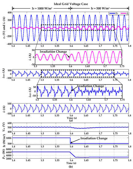
Figure 10.
Dynamic response at PCC during grid sharing and power conditioning; (a) ideal grid input voltage, current, MFI current, and load current; (b) MFI DC-link voltage, solar irradiation, and PV power under the ideal grid.
In the current response depicted in Figure 10a, there was a rise in amplitude during the irradiation change from 1000 W/m2 to 500 W/m2 at time t = 1.6 s because of the reduction in RTSPV power. This means the grid consumption was raised. However, the source current harmonics were compensated for successfully. The inverter current injected at the PCC, and the load current responses are illustrated in Figure 10a. The DC-link voltage and PV power concerning the variation in solar irradiation are described in Figure 10b at t = 1.6 s. Even though the solar irradiation was decreased, the MFI could supply the active power corresponding to that irradiation as per the INC-based MPPT characteristics. Thereby, the MFI was performing the grid sharing partially and power conditioning without interruption.
4.4.2. Distorted Grid Voltage Case
The dynamic response of the system during the solar irradiation change under the distorted grid condition is presented in Figure 11a,b. In this case, the current consumption from the grid was increased due to the reduction in PV power because of the irradiation change as shown in Figure 11a. However, the MFI executed the power conditioning effectively. The MFI was capable of extracting the maximum power with respect to the reduced irradiation as per the INC-based MPPT effectively. Thus, the MFI is successful in executing the multi-functional tasks simultaneously without interruption.
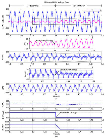
Figure 11.
Dynamic response at PCC during grid sharing and power conditioning; (a) distorted grid input voltage, current, MFI current, and load current; (b) MFI DC-link voltage, solar irradiation, and PV power under the distorted grid.
5. Real-Time Experimental Validation
In this section, the RT software in loop (SIL) testing of the proposed RTSPV MFI system interfaced to the LVDS is presented.
The proposed RTSPV integration system with the LVDS loads was modeled in the RT-LAB environment and tested in RT using the OP4500 RT grid simulator [41,42]. The main purpose of validating in RT is to understand the proposed MFI system behavior for real-world implementation. The OP4500 is one of the commercially available RT power grid simulators. The detailed architecture and specifications are illustrated in Reference [42]. The laboratory test setup for RT validation is shown in Figure 12.
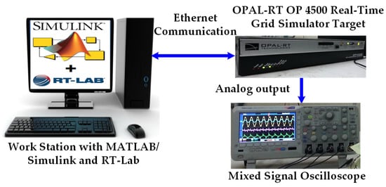
Figure 12.
Laboratory test setup of real-time (RT) software in loop (SIL) validation.
5.1. SIL RT Test Results of Mode 1: MFI OFF
The SIL RT test results of the LVDS during the MFI OFF condition are depicted in Figure 13. These responses are identical to the simulation results depicted in Figure 7, and showcase the harmonic and reactive power effects at the PCC of the LVDS under both ideal and distorted grid conditions. Hence, it is essential to improve the LVDS power quality for efficient and reliable operation.
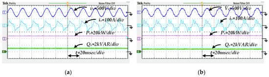
Figure 13.
RT SIL test waveforms under MFI OFF mode under (a) the ideal grid and (b) the distorted grid.
5.2. SIL RT Test Results of Mode 2: MFI is ON, with Grid Sharing and Power Conditioning
5.2.1. Ideal Grid Voltage Case
The SIL RT results of the MFI grid sharing and power conditioning mode are presented in Figure 14a–c. The RT results authenticate the simulated results of MFI grid sharing and power conditioning operations presented in Figure 8. Here, the source current harmonics were compensated, and the source voltage and source current were an in-phase nature. The compensated current injected at the PCC by the MFI to make the source current sinusoidal is presented in Figure 14a. However, the load draws the nonlinear current as shown in Figure 14a. The regulated DC-link voltage of 500 V and the RTSPV maximum power of 6 kW extracted at the solar irradiation of 1000 W/m2 are illustrated in Figure 14b. In Figure 14c, the active and reactive power profiles of the source and MFI are depicted. This enumerates the reduction of grid consumption from 9 kW to 3 kW. Furthermore, the source reactive power is reduced to zero by the MFI, as described in simulated results.
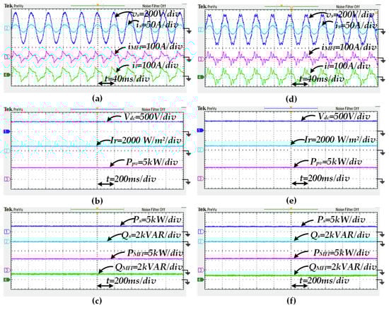
Figure 14.
RT SIL test output waveforms under the MFI ON, with grid sharing and power conditioning mode; (a) ideal grid input voltage, current, MFI current, and load current; (b) MFI DC-link voltage, solar irradiation, and PV power under the ideal grid; (c) source active power, reactive power, and MFI active and reactive power under the ideal grid; (d) distorted grid input voltage, current, MFI current, and load current; (e) MFI DC-link voltage, solar irradiation, and PV power under the distorted grid; (f) source active power, reactive power, MFI active and reactive power under the distorted grid.
The simulated DC-link voltage controller had high bandwidth and responded instantaneously, including to the high-frequency current harmonics flowing through the capacitor, observed by rapid variations in the DC-link voltage, as depicted in Figure 8. However, in the RT-implemented system, the DC-link voltage was discretized; the whole bandwidth decreased, and there was also moving-average filtering of the analog-to-digital converter (ADC) feedback signals. Therefore, the closed-loop response for such a DC-link voltage control loop was not so rapid, the capacitor voltage had fewer fluctuations, and had less ripple when compared to the simulated case-study, as observed in Figure 14. Such a smoother capacitor voltage in RT control is, indeed, a very desirable feature.
5.2.2. Distorted Grid Voltage Case
The RT results of the MFI grid sharing and power conditioning operation under the distorted grid condition are presented in Figure 14d–f. These RT results were identical to the simulated results of the MFI grid sharing and power conditioning mode. In this case, the source current was sinusoidal, and it was in-phase with the source voltage. However, the load behavior was nonlinear as illustrated in Figure 14d. The MFI current injected at the PCC to compensate for the harmonic distortion is described in Figure 14d. The DC-link voltage regulated at 500 V and the RTSPV maximum power of 6 kW extracted at the solar irradiation of 1000 W/m2 under the distorted grid are illustrated in Figure 14e, which are similar to the simulated results. In Figure 14f, the active and reactive power profiles of the source and MFI obtained by the RT simulation are illustrated. These profiles enumerate the reduction of grid consumption from 9 kW to 3 kW, as discussed in the simulated results. Furthermore, the reactive power effect was compensated for successfully.
5.3. SIL RT Test Results of Mode 3: MFI is ON, with Grid Feeding and Power Conditioning
5.3.1. Ideal Grid Voltage Case
The MFI grid feeding and power conditioning responses under the ideal grid case when the load consumption as reduced are described in Figure 15a–c. In this case, the MFI was feeding the load as well as the grid, simultaneously. Moreover, it as also taking care of the harmonic and reactive power compensation. The DC-link voltage regulated at 500 V and the reduced load power and reactive power responses are presented in Figure 15b. The active and reactive power profiles under grid feeding mode are depicted in Figure 15c. Here, the negative response of the active power represents the grid feeding operation; simultaneously, the reactive power at the source side was reduced to zero. The RT results are identical to the simulated results.
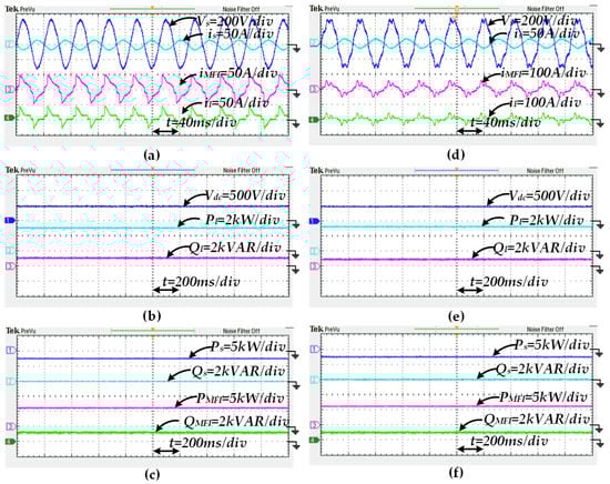
Figure 15.
RT SIL test output waveforms under MFI ON, with grid feeding and power conditioning mode; (a) ideal grid input voltage, current, MFI current, and load current; (b) MFI DC-link voltage, solar irradiation, and PV power under the ideal grid; (c) source active power, reactive power, and MFI active and reactive power under the ideal grid; (d) distorted grid input voltage, current, MFI current, and load current; (e) MFI DC-link voltage, solar irradiation, and PV power under the distorted grid; (f) source active power, reactive power, and MFI active and reactive power under the distorted grid.
5.3.2. Distorted Grid Voltage Case
The MFI grid feeding and power conditioning responses under the distorted grid case when the load consumption was reduced are described in Figure 15d–f. In this case, the MFI was feeding the load as well as the grid, simultaneously. Moreover, it as also taking care of the harmonic and reactive power compensation. The DC-link voltage regulated at 500 V and the reduced load power and reactive power responses are presented in Figure 15e. The active and reactive power profiles under the grid feeding mode are depicted in Figure 15f. Here, the negative response of the active power represents the grid feeding operation. Moreover, the reactive power at the source side was reduced to zero, simultaneously. The RT results are identical to the simulated results.
5.4. SIL RT Test Results of Mode 4: MFI is ON, with Grid Sharing and Power Conditioning during Irradiation Change
The pictorial representations of the dynamic source current variation during irradiation change under both the ideal and distorted grid conditions are represented in Figure 16a–d. Here, the source current magnitude was increased because of the drop in active power delivery from the MFI due to irradiation change from 1000 W/m2 to 500 W/m2. Figure 16 responses are identical to the simulation responses of Figure 10 and Figure 11. Hence, in RT it was also confirmed that the proposed RTSPV interfaced MFI performs the power conditioning and power injection for ideal and distorted supply conditions effectively during the irradiation change.
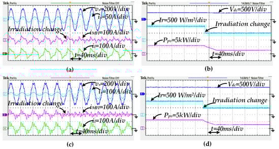
Figure 16.
RT SIL test dynamic response at PCC under grid sharing and power conditioning mode during Solar irradiation change (a) Ideal Grid Input Voltage, Current, MFI current and load current; (b) MFI DC-link voltage, solar Irradiation and PV power under ideal grid; (c) Distorted Grid Input Voltage, Current, MFI current and load current; (d) MFI DC-link voltage, solar Irradiation and PV power under distorted grid.
5.5. Active and Reactive Power Exchange
The summary of the active and reactive power profiles of the source, MFI, and loads obtained from the RT SIL test are tabulated in Table 6.
Table 6.
Active and reactive power summary under ideal and distorted grid conditions under Ir = 1000 W/m2.
6. Discussion
In this section, the detailed summary of the SIL RT results of the proposed RTSPV integration system and its comparison with the VDB-HCC method presented in Reference [30] are discussed.
6.1. Switching Frequency
The instantaneous switching frequency values of the VDB-HCC and the proposed MB-HCC are calculated concerning the switching frequency formula given in Reference [40]. The instantaneous average switching frequency of the MFI using MB-HCC was maintained at 10 kHz, whereas the VDB-HCC [30] had 16 kHz under nonlinear load conditions. The precise tracking of the current in between the two bands (HB1 and HB2) and the corresponding switching logic of the MFI resulted in a reduction of MFI switching frequency.
6.2. MFI Efficiency
The MFI efficiency concerning the solar irradiation under both full load and reduced load conditions using VDB-HCC [30] are presented in Figure 17.
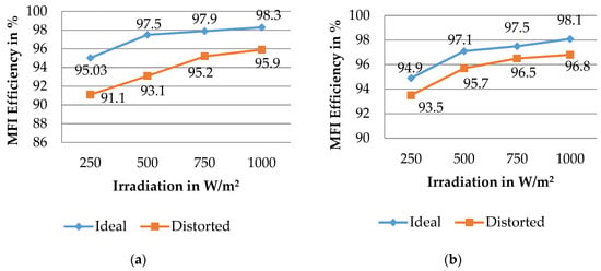
Figure 17.
MFI efficiency using VDB-HCC: (a) full load; (b) reduced load.
The MFI had a peak efficiency of 98.3% and an average efficiency of 97.18% under the ideal grid condition at full load. In a distorted grid case, the MFI had a peak efficiency of 95.9% and an average efficiency of 93.82% at full load condition. In the reduced load case, the MFI had a peak efficiency of 98.1% and an average efficiency of 96.9% under the ideal grid voltage case, whereas in the distorted grid condition, the peak efficiency was 96.9% and average efficiency was 95.62%.
The MFI efficiency variation concerning the solar irradiation under both the full load and reduced load conditions using MB-HCC are presented in Figure 18. The peak efficiency of the MFI was 99.01%, and the average MFI efficiency under the ideal grid voltage was 98.77% at the fully loaded condition, whereas in the distorted grid voltage case, the peak efficiency was 98.5% and average efficiency was 97.56%.
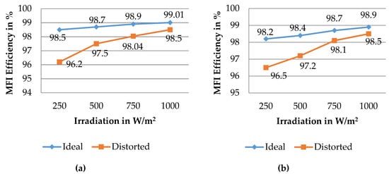
Figure 18.
MFI efficiency using MB-HCC: (a) Full Load; (b) Reduced Load.
During the reduced load case, the peak efficiency of the MFI was 98.9%, and the average MFI efficiency under the ideal grid voltage was 98.55%. In a distorted grid voltage condition, the peak efficiency was 98.5%, and the average efficiency was 97.57%. This means that the MFI exhibited better efficiency using MB-HCC under both ideal and distorted grid voltage conditions when compared to the VDB-HCC method. The MFI inverter efficiency was reasonable under the lower irradiation case when compared to the VDB-HCC method. However, in the proposed MB-HCC method, the MFI efficiency under the lower irradiation condition (i.e., <500 W/m2) in a distorted grid case was slightly lower when compared to the peak efficiency of the MFI at irradiation >500 W/m2, but the power conditioning task performed effectively as per the requirements of IEEE 519-2014 and IEEE 1547. This was because, under the lower irradiation case, the MB-HCC based MFI was more efficient in compensating for the highest percentage THD when compared to the ideal voltage case nonlinear load percentage THD.
6.3. Percentage THD at Point Common Coupling
The %THD at PCC during no compensation and with MFI compensation cases under ideal and distorted grid voltage conditions using the VDB-HCC method [30] is illustrated in Figure 19. The %THD was brought down from 34.08% to 3.56% under the ideal voltage condition at full load. For the reduced load case, it as reduced from 53.79% to 3.19%. In a distorted grid voltage condition, the %THD was reduced from 42.69% to 2.64% at full load case. In the reduced load case, the %THD was minimized from 64.5% to 3.4%.
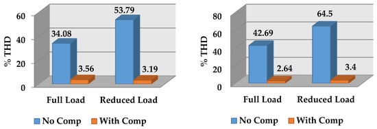
Figure 19.
%THD at PCC using VDB-HCC: (a) ideal grid condition; (b) distorted grid condition.
The %THD comparison at PCC during no compensation and with MFI compensation using MB-HCC method under ideal and distorted grid conditions are depicted in Figure 20. The %THD at full load was brought down from 34.08% to 2.34% under the ideal grid condition, whereas in the half load case it was reduced from 53.79% to 2.98%. In a distorted grid condition, the %THD was reduced from 42.69% to 2.04% under the full load case. In the reduced load case, the %THD was minimized from 64.5% to 2.77%. The %THD results using VDB-HCC [30] and the proposed MB-HCC methods comply with the IEEE 519-2014 and 1547 standards.
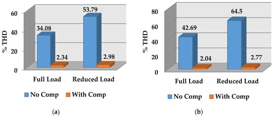
Figure 20.
%THD at PCC using MB-HCC: (a) ideal grid condition; (b) distorted grid condition.
6.4. True Power Factor at Point Common Coupling
The true power factor (TPF) at PCC before and after compensation of reactive power, under ideal and distorted grid voltage conditions, using the VDB-HCC [30] method is described in Figure 21. Under the ideal grid voltage condition, the TPF was improved from 0.9407 to 0.9993 at full load, whereas in the half load case it was improved from 0.8379 to 0.9990. In a distorted grid condition, the TPF was enhanced from 0.9174 to 0.9996 at full load. In the reduced load case, the TPF was enhanced from 0.816 to 0.9989. The power factor (PF) at PCC before and after compensation of reactive power, under ideal and distorted grid voltage conditions, using the MB-HCC method, are described in Figure 22.
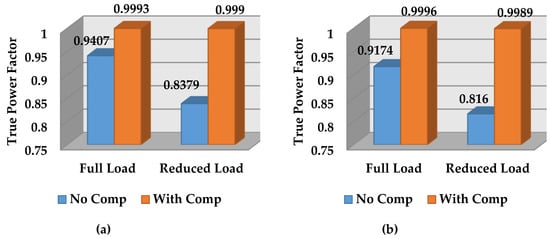
Figure 21.
True power factor at PCC using VDB-HCC: (a) ideal grid condition; (b) distorted grid condition.
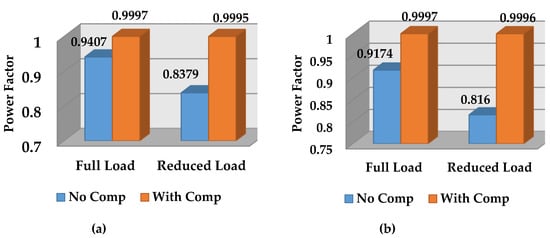
Figure 22.
True power factor at PCC using MB-HCC: (a) ideal grid condition; (b) distorted grid condition.
The TPF was improved from 0.9407 to 0.9997 at full load under the ideal grid voltage, whereas in the half load case it was improved from 0.8379 to 0.9995. The TPF under the distorted grid condition was enhanced from 0.9174 to 0.9997 at the full load case. In the reduced load case, the TPF was enhanced from 0.816 to 0.9996. Given the TPF results of the VDB-HCC and MB-HCC methods, both will maintain the TPF close to the unity value.
From the summary of the results presented in Table 7, it is justified that the MFI efficiently performs the power feeding at PCC as per the solar irradiation and compensates the source harmonics and reactive power with reduced switching frequency as per the IEEE 519-2014 and IEEE-1547 standards. These results exhibit the scalability and feasibility of the proposed system in LVDS under ideal and distorted grid conditions.
Table 7.
RT results summary.
7. Conclusions
This research article has demonstrated a two-stage RTSPV integration system using a DC-DC boost converter with INC-based MPPT and single-phase MFI with the proposed scaling factor-based MB-HCC method. The importance of the RTSPV interfaced MFI for grid sharing and feeding capabilities were investigated by a MATLAB/Simulink simulation and validated with OPAL-RT results. The proposed MB-HCC triggers insulated-gate bipolar transistor (IGBT) switches of the MFI through tracking current response between inner and outer hysteresis bands, leading to reduced switching frequency which, in turn, reduces switching losses. The RT results enumerated the potential of the proposed system regarding efficiency and improved PQ capabilities as per IEEE 519-2014 and IEEE 1547 standards. During the variation of solar irradiation, the proposed MFI had a peak efficiency of 99.01% and an average output efficiency of 98.77% under the ideal grid, and in the distorted grid case the peak efficiency was 98.5%, and the average efficiency was 97.31%. Moreover, the percentage of total harmonic distortion under ideal and distorted grid conditions was brought down to below 5%, and reactive power compensation was effective, resulting in unity power factor operation. The MFI efficiency under the full load condition was elevated by the proposed MB-HCC over the VDB-HCC by 1% under the ideal grid condition and 4% in the distorted grid condition. In the reduced load condition, the MFI efficiency was raised by the proposed MB-HCC over the VDB-HCC by 2%, under both ideal and distorted grid conditions. MB-HCC is scalable for variations in the solar irradiation and efficient over the VDB-HCC. The average percentage of THD was reduced up to 2.75%, and the source side power factor was close to unity. The simulation and RT results substantiate the hypothesis of higher efficiency and scalability of the MB-hysteresis current controlled MFI for a single-phase LVDS. The proposed two-stage MFI with MB-HCC is a unified solution to reduce grid consumption and maintain the PQ of the single-phase LVDS, and hence it is ideal for adoption in support of global green energy initiative.
Author Contributions
V.S.R.V.O. contributed to the overall concept development, conceptualization, and performed the experiments. V.S.S.S.S.D. performed the supervision and contributed to the resources. V.S.R.V.O. contributed to the writing of the original draft. V.S.S.S.S.D. and M.G.S. contributed to professional advice, writing—review, and editing the draft; all authors have read and approved the final manuscript.
Funding
This research received no external funding.
Acknowledgments
The authors gratefully acknowledge the Department of Electrical Engineering, National Institute of Technology Warangal, INDIA for providing necessary facilities and the Advanced Control of Energy Power Systems (ACEPS) research group of Electrical Engineering Department at Colorado School of Mines, USA for their support.
Conflicts of Interest
The authors declare no conflict of interest.
Nomenclature
| A | Boltzmann’s constant | Ir | Irradiance |
| CB | Circuit Breaker | Ls | Source inductance |
| Cdc | DC-link capacitor | LMFI | MFI interfacing inductance |
| Cpv | PV side boost stage capacitor | Lb | Boost stage inductor |
| Db | Boost stage Diode | Ps | Source active power |
| D | Duty cycle | Pl | Load active power |
| fsw | Switching Frequency of the MFI | PMFI | Active power from MFI |
| hmin | Minimum Hysteresis Band | Ppv | Active power generated from SPV |
| H | Maximum Hysteresis Band | PI | Proportional Integral Controller |
| km | Modulation Index | Qs | Source reactive power |
| HB1 | Main Hysteresis Band | Ql | Load reactive power |
| HB2 | Sub Hysteresis Band | QMFI | Reactive power from MFI |
| h1 | Scaling Factor 1 | q | Electron charge |
| h2 | Scaling Factor 2 | Rs | Source resistance |
| is | Source current | Rse | Single diode model series resistance |
| isref | Reference current | Rp | Single diode model Parallel resistance |
| iMFI | MFI current | S1, S2, S3, S4 | IGBT Switches |
| il | Load current | Sb | Boost stage IGBT switch |
| im | Peak value of the source current | T | Junction temperature in Kelvin |
| Isc | Short circuit current | Us | Unit vector template |
| Irtpv | Rooftop PV output current | vs | Source voltage |
| Id | Current through the Diode | vMFI | MFI output voltage |
| Isat | Saturation current | Vdc | DC-link voltage |
| Imp | Current at maximum power | Vdc | Reference DC-link voltage |
| Ip | Current through the Parallel resistance | Vdc | DC-link voltage error |
| Iph | Photovoltaic current | Vrtpv | Rooftop-PV output DC voltage |
| k | Ideality factor of the diode | Vmp | Voltage at maximum power |
| kp | Proportional Gain | Voc | Open circuit voltage |
| ki | Integral Gain | Vrtpv | Rooftop-PV output DC voltage |
References
- Nicholls, A.; Sharma, R.; Saha, T.K. Financial and environmental analysis of rooftop photovoltaic installations with battery storage in Australia. Appl. Energy 2015, 159, 252–264. [Google Scholar] [CrossRef]
- Cole, W.; Lewis, H.; Sigrin, B.; Margolis, R. Interactions of rooftop PV deployment with the capacity expansion of the bulk power system. Appl. Energy 2016, 168, 473–481. [Google Scholar] [CrossRef]
- Sundaray, S.; Mann, L.; Bhattacharjee, U.; Garud, S.; Tripathi, A.K. Reaching the Sun with Rooftop Solar; The Energy and Resources Institute (TERI): New Delhi, India, 2014; 62p. Available online: http://mnre.gov.in/file-manager/UserFiles/Rooftop-SPV-White-Paper-low.pdf (accessed on 16 June 2018).
- Bhati, P.; Kalsotra, R. Solar Rooftop: Replacing Diesel Generators in Residential Societies; Centre for Science and Environment: New Delhi, India, 2017; Available online: http://cseindia.org/userfiles/Policy-Brief-Solar-Rooftop-Replacing-Diesel-Generators-in-Residential-Societies.pdf (accessed on 16 June 2018).
- Deambi, S. Photovoltaic System Design: Procedures, Tools and Applications, 1st ed.; CRC Press: Boca Raton, FL, USA, 2016; pp. 1–280. ISBN 9781482259810. [Google Scholar]
- Fekete, K.; Klaic, Z.; Majdandzic, L. Expansion of the residential photovoltaic systems and its harmonic impact on the distribution grid. Renew. Energy 2012, 43, 140–148. [Google Scholar] [CrossRef]
- Yang, Y.; Zhou, K.; Blaabjerg, F. Current harmonics from single-phase grid-connected inverters—Examination and suppression. IEEE J. Emerg. Sel. Top. Power Electron. 2016, 4, 221–233. [Google Scholar] [CrossRef]
- Boynuegri, A.R.; Uzunoglu, M.; Erdinç, O.; Gokalp, E. A new perspective in grid connection of electric vehicles: Different operating modes for elimination of energy quality problems. Appl. Energy 2014, 132, 435–451. [Google Scholar] [CrossRef]
- Francisco, C. Harmonics, Power Systems, and Smart Grids, 2nd ed.; CRC Press: Boca Raton, FL, USA, 2015; pp. 1–278. ISBN 9781482243833. [Google Scholar]
- Zeng, Z.; Yang, H.; Zhao, R.; Cheng, C. Topologies and control strategies of multi-functional grid-connected inverters for power quality enhancement: A comprehensive review. Renew. Sustain. Energy Rev. 2013, 24, 223–270. [Google Scholar] [CrossRef]
- Rangarajan, S.S.; Collins, E.R.; Fox, J.C.; Kothari, D.P. A survey on global PV interconnection standards. In Proceedings of the Power and Energy Conference at Illinois (PECI), Champaign, IL, USA, 23–24 February 2017; pp. 1–8. [Google Scholar] [CrossRef]
- Kjaer, S.B.; Pedersen, J.K.; Blaabjerg, F. A review of single-phase grid-connected inverters for photovoltaic modules. IEEE Trans. Ind. App. 2005, 41, 1292–1306. [Google Scholar] [CrossRef]
- Yang, Y.; Blaabjerg, F. Overview of Single-phase Grid-connected Photovoltaic Systems. Electr. Power Compon. Syst. 2015, 43, 1352–1363. [Google Scholar] [CrossRef]
- Panda, A.; Pathak, M.K.; Srivastava, S.P. Enhanced power quality based single phase photovoltaic distributed generation system. Int. J. Electron. 2016, 103, 1262–1278. [Google Scholar] [CrossRef]
- Saxena, H.; Singh, A.; Rai, J.N. Design and performance analysis of generalised integrator-based controller for grid connected PV system. Int. J. Electron. 2018, 105, 1079–1096. [Google Scholar] [CrossRef]
- Deo, S.; Jain, C.; Singh, B. A PLL-less scheme for single-phase grid interfaced load compensating solar PV generation system. IEEE Trans. Ind. Inf. 2015, 11, 692–699. [Google Scholar] [CrossRef]
- Gupta, A.; Chauhan, Y.K.; Pachauri, R.K. A comparative investigation of maximum power point tracking methods for solar PV system. Sol. Energy 2016, 136, 236–253. [Google Scholar] [CrossRef]
- De Brito, M.A.G.; Galotto, L.; Sampaio, L.P.; Melo, G.D.A.; Canesin, C.A. Evaluation of the main MPPT techniques for photovoltaic applications. IEEE Trans. Ind. Electr. 2013, 60, 1156–1167. [Google Scholar] [CrossRef]
- Cupertino, A.F.; Pereira, H.A.; da Costa, W.U.; Silva, S.R. Multifunctional Inverters Applied in Grid-Connected Photovoltaic Systems. In Proceedings of the Fifth Brazilian Symposium on Electrical Systems—SBSE, Foz do Iguaçu—Paraná, Brazil, 22–25 April 2014; pp. 1–7. [Google Scholar] [CrossRef]
- Xavier, L.S.; Cupertino, A.F.; Pereira, H.A. Ancillary services provided by photovoltaic inverters: Single and three phase control strategies. Comput. Electr. Eng. 2018, 1–20. [Google Scholar] [CrossRef]
- Chatterjee, A.; Mohanty, K.; Kommukuri, V.S.; Thakre, K. Design and experimental investigation of digital model predictive current controller for single phase grid integrated photovoltaic systems. Renew. Energy 2017, 108, 438–448. [Google Scholar] [CrossRef]
- Kim, I.S. Sliding mode controller for the single-phase grid-connected photovoltaic system. Appl. Energy 2006, 83, 1101–1115. [Google Scholar] [CrossRef]
- Rahim, N.A.; Selvaraj, J. Implementation of hysteresis current control for single-phase grid connected inverter. In Proceedings of the 7th International Conference on Power Electronics and Drive Systems (PEDS), Bangkok, Thailand, 27–30 November 2007; pp. 1097–1101. [Google Scholar] [CrossRef]
- Martins, A.; Vale, S.; Sobrado, V.; Carvalho, A. Comparison of current control methods for grid-connected low-power single-phase converters. In Proceedings of the 40th Annual Conference of the IEEE Industrial Electronics Society (IECON), Dallas, TX, USA, 29 October–1 November 2014; pp. 4211–4217. [Google Scholar] [CrossRef]
- Patidar, R.D.; Singh, S.P.; Khatod, D.K. Single-phase single-stage grid-interactive photovoltaic system with active filter functions. In Proceedings of the Power and Energy Society General Meeting, Providence, RI, USA, 25–29 July 2010; pp. 1–7. [Google Scholar] [CrossRef]
- Helal, A.; Nour, A.; El-Mohr, I. Multifunctional Single-Phase Single-Stage Grid-Connected PV System. In Proceedings of the International Conference on Renewable Energies and Power Quality (ICREPQ’12), Santiago de Compostela, Spain, 28–30 March 2012; pp. 1–6. [Google Scholar] [CrossRef]
- Sahoo, P.K.; Ray, P.K.; Das, P. Power quality improvement of single phase grid connected photovoltaic system. Int. J. Emerg. Electr. Power Syst. 2017, 18. [Google Scholar] [CrossRef]
- Singh, Y.; Hussain, I.; Singh, B.; Mishra, S. Implementation of grid interfaced photovoltaic system with active power filter capabilities. Int. Trans. Electr. Energy Syst. 2018. [Google Scholar] [CrossRef]
- Dahono, P.A. New hysteresis current controller for single-phase full-bridge inverters. IET Power Electron. 2009, 2, 585–594. [Google Scholar] [CrossRef]
- Priandana, E.R.; Saputra, M.; Prabowo, Y.; Dahono, P.A. Analysis and design of variable double-band hysteresis current controller for single-phase full-bridge bidirectional converters. In Proceedings of the International Symposium on the Technology Management and Emerging Technologies (ISTMET), Bandung, Indonesia, 27–29 May 2014; pp. 143–148. [Google Scholar] [CrossRef]
- Komurcugil, H. Double-band hysteresis current-controlled single-phase shunt active filter for switching frequency mitigation. Int. J. Electr. Power Energy Syst. 2015, 69, 131–140. [Google Scholar] [CrossRef]
- IEEE 519-2014 Standard. Recommended Practice and Requirements for Harmonic Control in Electric Power Systems; (Revision of IEEE Std 519–1992); IEEE: New York, NY, USA, 2014; pp. 1–29. [CrossRef]
- Koutroulis, E.; Blaabjerg, F. Overview of maximum power point tracking techniques for photovoltaic energy production systems. Electr. Power Compon. Syst. 2015, 43, 1329–1351. [Google Scholar] [CrossRef]
- SolardesignTool. Available online: http://www.solardesigntool.com/components/module-panelsolar/Sunpower/514/SPR-305-WHT U/specification-data-sheet.html (accessed on 16 March 2018).
- Mohamed, T.L.; Mohamed, R.H.; Mohamed, Z. Development of auto tuning PID controller using graphical user interface (GUI). In Proceedings of the Second International Conference on Computer Engineering and Applications (ICCEA-2010), Bali Island, Indonesia, 19–21 March 2010; pp. 491–495. [Google Scholar] [CrossRef]
- Garrido, J.; Ruz, M.; Morilla, F.; Vázquez, F. Interactive Tool for Frequency Domain Tuning of PID Controllers. Processes 2018, 6, 197. [Google Scholar] [CrossRef]
- Yang, Y.; Hadjidemetriou, L.; Blaabjerg, F.; Kyriakides, E. Benchmarking of phase locked loop based synchronization techniques for grid-connected inverter systems. In Proceedings of the 9th International Conference on Power Electronics and ECCE Asia (ICPE ECCE Asia), Seoul, Korea, 1–5 June 2015; pp. 2517–2524. [Google Scholar] [CrossRef]
- Zhang, Z.; Yang, Y.; Ma, R.; Blaabjerg, F. Zero-voltage ride-through capability of single-phase grid-connected photovoltaic systems. Appl. Sci. 2017, 7, 315. [Google Scholar] [CrossRef]
- Mathworks Home page. Available online: https://in.mathworks.com/help/physmod/sps/powersys/ref/pll.html (accessed on 16 July 2018).
- Gautam, S.; Gupta, R. Unified time-domain formulation of switching frequency for hysteresis current controlled AC/DC and DC/AC grid connected converters. IET Power Electron. 2013, 6, 683–692. [Google Scholar] [CrossRef]
- Belanger, J.; Venne, P.; Paquin, J.N. The what, where and why of real-time simulation. Planet RT 2010, 1, 37–49. [Google Scholar]
- OPAL-RT OP4500/4510. Available online: https://www.opal-rt.com/wp-content/themes/enfold-opal/pdf/L00161_0124.pdf (accessed on 9 August 2018).
© 2019 by the authors. Licensee MDPI, Basel, Switzerland. This article is an open access article distributed under the terms and conditions of the Creative Commons Attribution (CC BY) license (http://creativecommons.org/licenses/by/4.0/).