Article

Gallium Nitride Normally-Off Vertical Field-Effect Transistor Featuring an Additional Back Current Blocking Layer Structure

1
School of Optoelectronic Engineering and Instrumentation Science, Dalian University of Technology, Dalian 116024, China
2
Key Laboratory for Micro/Nano Technology and System of Liaoning Province, Dalian University of Technology, Dalian 116024, China
3
Key Laboratory of Semiconductor Materials Science & Beijing Key Laboratory of Low Dimensional Semiconductor Materials and Devices, Institute of Semiconductors, Chinese Academy of Sciences, Beijing 100083, China
*
Author to whom correspondence should be addressed.
Electronics 2019, 8(2), 241; https://doi.org/10.3390/electronics8020241
Submission received: 31 December 2018 / Revised: 12 February 2019 / Accepted: 18 February 2019 / Published: 20 February 2019
(This article belongs to the Special Issue Nanoelectronic Materials, Devices and Modeling)

Abstract

:
A gallium nitride (GaN) semiconductor vertical field-effect transistor (VFET) has several attractive advantages such as high power density capability and small device size. Currently, some of the main issues hindering its development include the realization of normally off operation and the improvement of high breakdown voltage (BV) characteristics. In this work, a trenched-gate scheme is employed to realize the normally off VFET. Meanwhile, an additional back current blocking layer (BCBL) is proposed and inserted into the GaN normally off VFET to improve the device performance. The electrical characteristics of the proposed device (called BCBL-VFET) are investigated systematically and the structural parameters are optimized through theoretical calculations and TCAD simulations. We demonstrate that the BCBL-VFET exhibits a normally off operation with a large positive threshold voltage of 3.5 V and an obviously increased BV of 1800 V owing to the uniform electric field distribution achieved around the gate region. However, the device only shows a small degradation of on-resistance (RON). The proposed scheme provides a useful reference for engineers in device fabrication work and will be promising for the applications of power electronics.

1. Introduction

With the rapid development of the power electronics industry, Si- or GaAs-based devices are approaching their material limit. The wide-bandgap semiconductors (known as third-generation semiconductors) have been widely employed and developed owing to their excellent physical properties such as large bandgap and high critical breakdown electric field. Among them, gallium nitride (GaN) is regarded as one of the most promising candidates for application in next-generation power devices [1,2], which is mainly due to the existence of high-density two-dimensional electron gas (2-DEG) in the AlGaN/GaN heterojunction interface induced by the strong polarization effect in wurtzite GaN [3,4]. Hence, the on-resistance (RON) and switching frequency of the power devices are improved dramatically.
GaN-based lateral high electron mobility transistor (HEMT) devices have been extensively demonstrated and have made great progress in the past few decades [5,6,7,8]. However, these lateral devices still encounter a few issues such as power density limit and output current collapse. For example, to improve the breakdown voltage (BV), the gate-to-drain distance of the HEMT has to be increased; this results in an obvious increase of the RON. Meanwhile, the peak electric field is located at the drain-side gate corner of the HEMT surface, which also leads to a limiting of the device output characteristics and a serious reliability issue when operated under high voltage [9,10]. Another challenge in lateral GaN-based HEMT is how to make the normally off device. Actually, normally off operation is strongly desired for safety and for efficient power switching in the integrated circuits (ICs) or systems for better compatibility. However, a standard AlGaN/GaN HEMT is naturally normally on because of the presence of the 2-DEG channel. Recently, various approaches such as gate-recess etching [5,7], fluorine-ion implantation [10], and p-cap layer deposition [6] have been explored to realize the normally off operation. However, it is still a big challenge to simultaneously obtain a high positive threshold voltage (Vth) and a large drain output current for an HEMT.
To overcome the mentioned issues, GaN vertical field-effect transistor (VFET) devices have been proposed and developed recently [11,12,13,14,15]. The drain electrode of the device is moved to the back of the wafer and, hence, the main electric field and conducting current flow are turned to the vertical direction. The peak point of the electric field is transferred into the bulk where the defect density is less and the crystal quality is better. Furthermore, the field distribution is more uniform. Therefore, the device current collapse is alleviated and the BV characteristics can be improved. Recently, some work has been conducted on normally on VFET devices and significant progress has been achieved. However, there is still a lack of sufficient research on the normally off VFET devices and, in particular, on their design and demonstration to improve the high voltage characteristics. Therefore, GaN power devices featuring both vertical structure and normally off operation will be very promising in the future applications of power electronics, and novel structure design and effective process technology are thus needed.
In this work, an additional back current blocking layer (BCBL) is introduced and inserted into the GaN normally off VFET to improve the BV characteristics. The electrical characteristics of the proposed device (called BCBL-VFET in this work) are investigated and the structural parameters are optimized through theoretical calculations and TCAD simulation work. Firstly, the pn-junction device was fabricated, and the measured I–V characteristics were employed to calibrate the physical parameters of the proposed device in the theoretical calculation and simulation work. Then the distribution characteristics of the electric field and impact ionization concentration were analyzed. Improved BV and RON were achieved after optimizing the thickness, depth, and spatial location of the current blocking layer in the GaN BCBL-VFET.

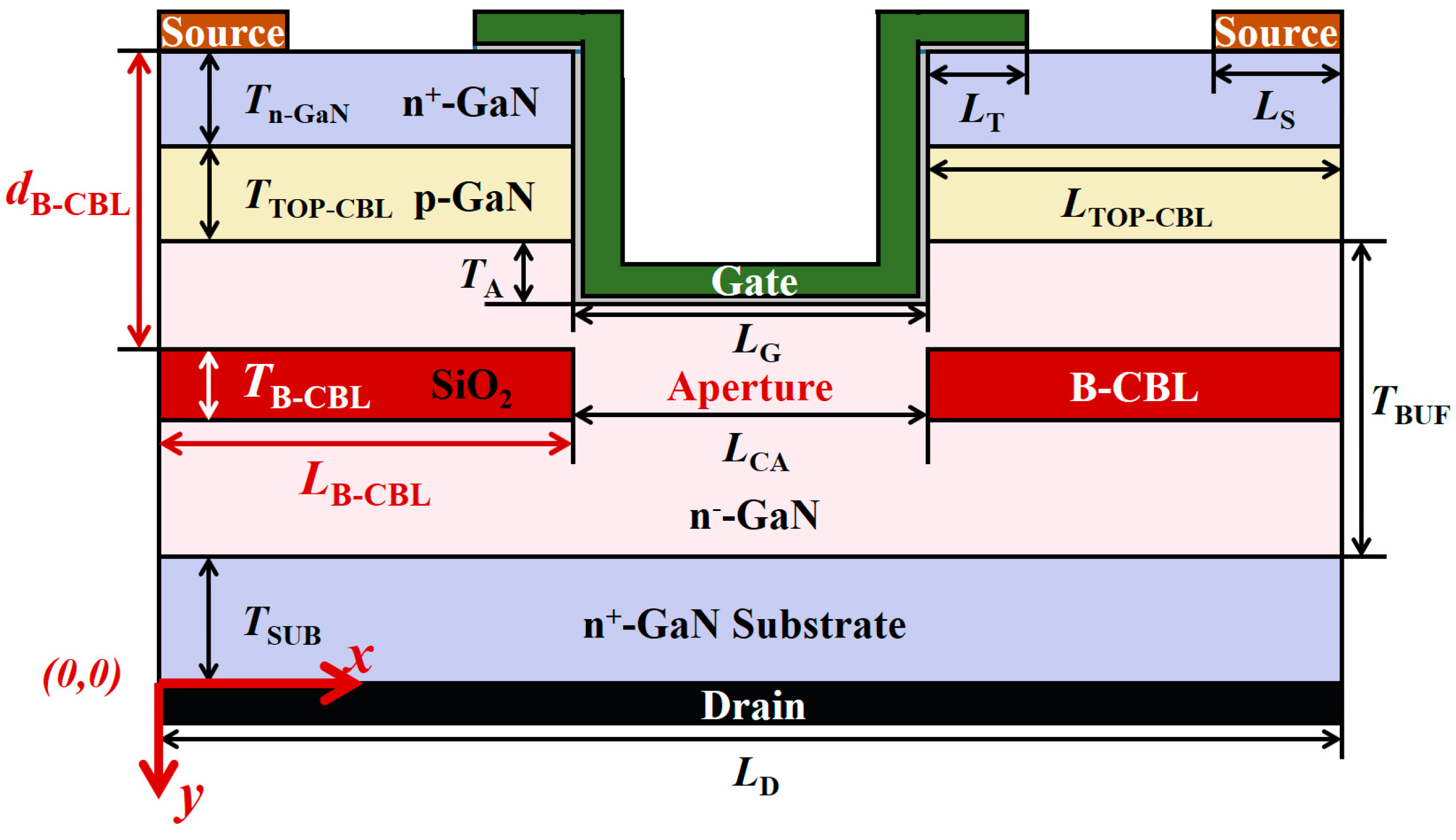
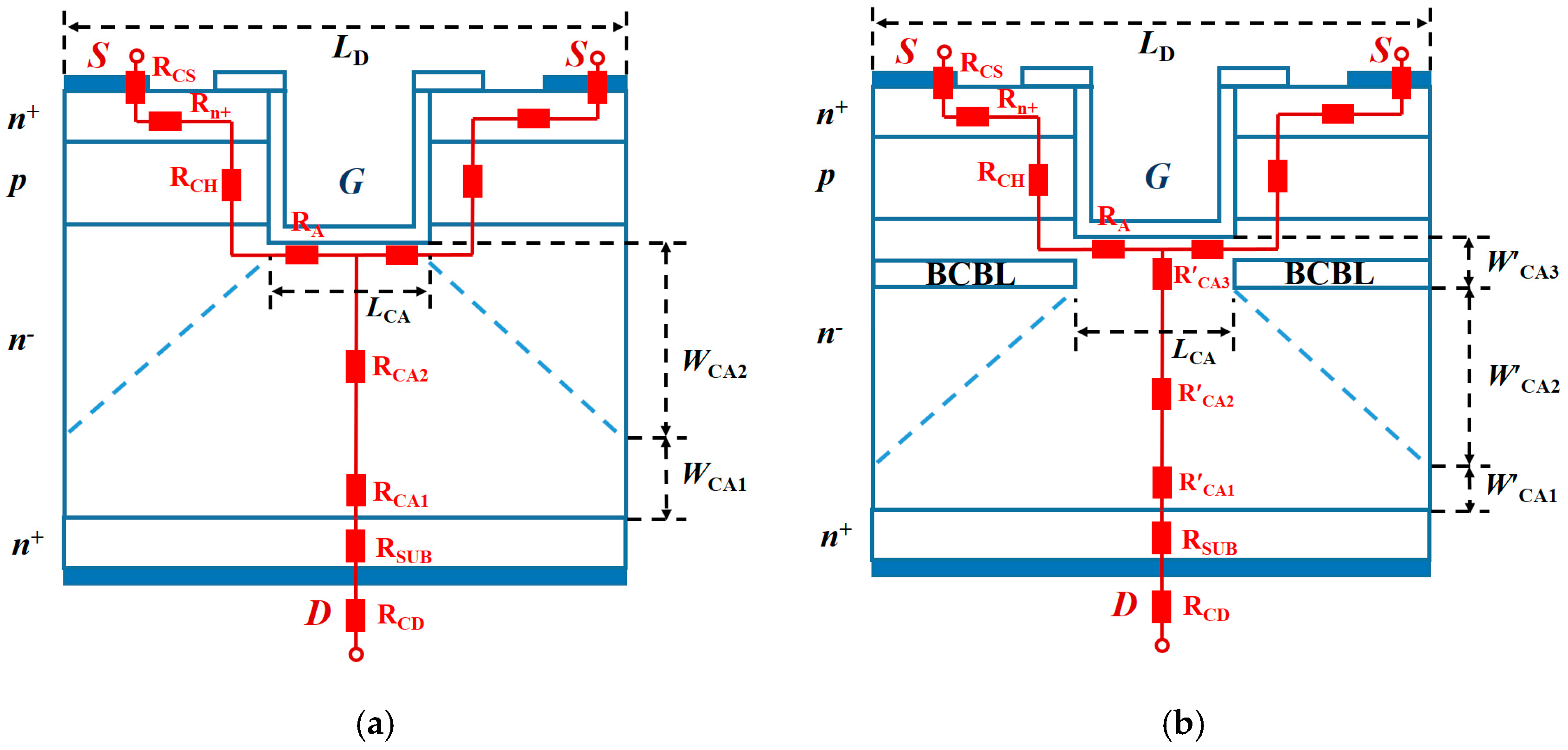
2. The Device Structure

Figure 1 shows the cross-sectional schematic of the proposed GaN BCBL-VFET. The key feature which is different from the conventional one is the introduction of the BCBL below the normal current blocking layer under the source electrode. The specifics of the device structure are listed in Table 1. In the conventional VFET, the breakdown points usually occur at the top pn-junction or at the etched gate corner under high-voltage operation because of the presence of high peak electric field. The additional insertion of the insulated BCBL will distribute the vertical voltage drop and also alleviate the crowding of the electric field around the gate corner. Hence, the BV of the proposed device will be improved significantly. Considering that the device still remains a good vertical current aperture, the output characteristics will not be degraded seriously. The structural parameters of the proposed BCBL such as the thickness, depth, and spatial location will be optimized by the theoretical calculation and simulation work, in detail.

3. Fabrication Work and Parameter Calibration

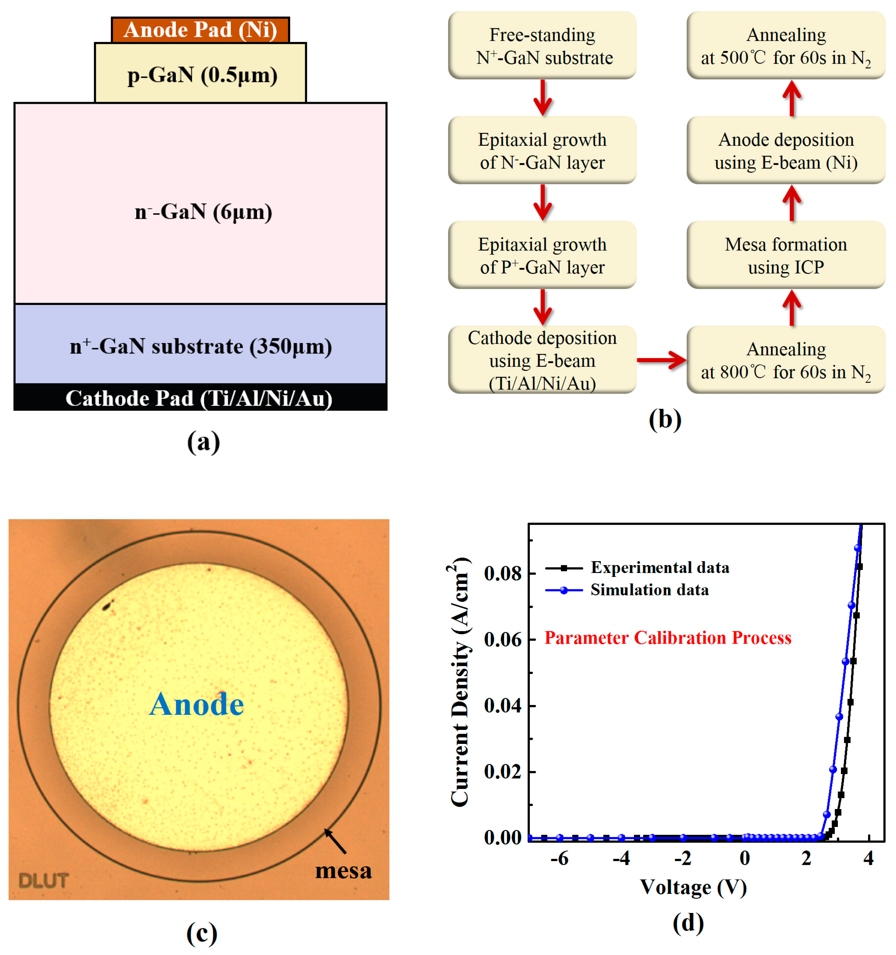
3.1. Fabrication Process of the PN-Junction Devices

The GaN pn-junction was grown on a 350 μm GaN free-standing substrate using a metal organic chemical vapor deposition (MOCVD) system. The doping concentration of n+-GaN substrate was 5 × 1018 cm–3. The epitaxial structure consisted of a 6 μm n-GaN layer with a background n-type carrier concentration of 5 × 1016 cm–3 and a 500 nm p-GaN layer with an Mg doping concentration of 3 × 1019 cm–3. The schematic cross-section, process flow, and top view of the fabricated GaN pn-junction device are shown in Figure 2. The Ti/Al/Ni/Au n-type ohmic contact was first formed on the back of the substrate by electron beam evaporation and annealing treatment under 800 ℃ for 60 s in N2 atmosphere. Edge termination was realized by mesa etching using an inductively coupled plasma (ICP) system under an ambience consisting of Cl2 and BCl3 mixed gas. The etching process was continued for 100 s. The Ni p-type ohmic contact was then formed on the p-GaN epitaxial layer also by electron beam evaporation. The annealing temperature was 500 ℃. The diameter of the anode pad was around 400 μm and the photo is shown in Figure 2c.

3.2. Parameter Calibration Process

The I–V characteristics of the pn-junction device were measured by a semiconductor characterization system (Keithley 4200) at room temperature for the purpose of the subsequent parameter calibration. In the TCAD simulation section, similar device configuration and structural parameters were employed. The physical parameters used in the simulations were calibrated by benchmarking the simulated I–V characteristics of the GaN pn-junction device with the experimental data. Figure 2d shows the comparisons of I–V curves which clearly indicates a good data match. Table 2 lists the employed physical parameters after calibration.
To accurately simulate the device behaviors, appropriate physical models must be selected. In this work, the Shockley–Read–Hall (SRH) model was employed to govern the charge-trapping behavior. The Arora model was employed to determine the doping-dependent mobility for the low-field case. Furthermore, the Canali model was used for the high-field case considering that the carrier drift velocity is no longer proportional to the electric field, instead, the velocity saturates to a finite speed under high voltage. To simulate the off-state breakdown characteristics of power devices, the van Overstraeten–de Man model was used to generate the avalanche induced electron–hole pairs.

4. Results and Discussion

4.1. Parameter Optimization of the BCBL

The pn-junction in the GaN BCBL-VFET acts as the top current blocking layer (TCBL) to sustain the main bias voltage between the drain and source electrodes, which is similar to the case in the conventional VFET. The doping concentration of 8 × 1017 cm–3 and thickness of 0.75 μm were employed for the p-GaN layer based on the previous optimal data in the VFET. The concentrations of 5 × 10¹⁸ and 1.75 × 1016 cm–3 were employed for the upper n+-GaN and the lower n-GaN layers, respectively, and the thicknesses of 0.25 and 10 μm were kept for them in the BCBL-VFET for the following simulations.
There are three important structural parameters in the BCBL, i.e., dBCBL (the distance between the source and the BCBL), LBCBL (the length of the BCBL), and TBCBL (the thickness of the BCBL). They will all be optimized systematically by analyzing the BV and RON characteristics of the BCBL-VFET. Considering the trade-off between the BV and RON, a figure of merit (FOM = BV2/RON) value is employed to evaluate the comprehensive device performance. The optimization work for the parameters dBCBL, LBCBL, and TBCBL is discussed as below.

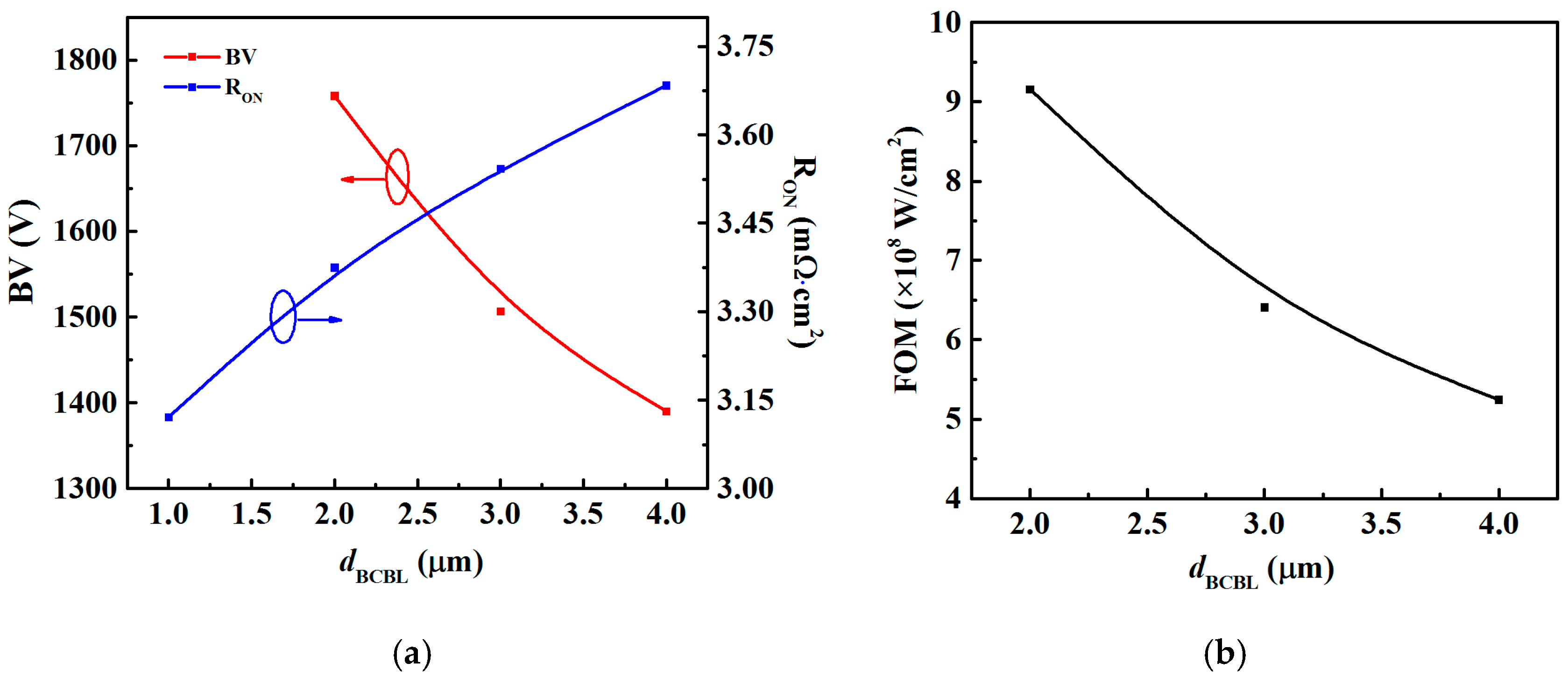
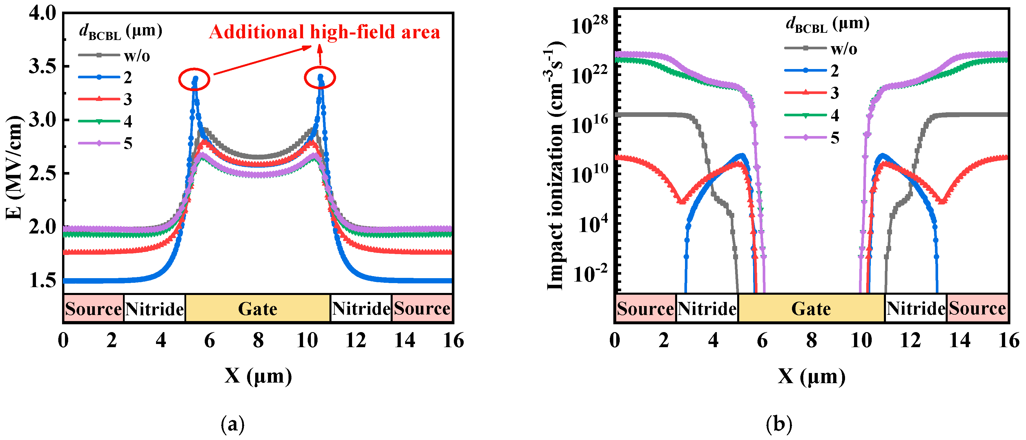
4.1.1. Optimization of dBCBL

The simulated BV and RON data and the calculated FOM values are shown in Figure 3a,b, respectively. It is clear that the BV is increased obviously when the BCBL approaches the gate. All the devices with additional BCBL exhibit obviously improved off-state characteristics. The BV value is more than 1380 V, while the conventional VFET with only TCBL shows a BV value around 1300 V. Moreover, the RON variations in the proposed devices are small even though the BCBL is very close to the gate (the reason will be explained and discussed in detail later). This proves the feasibility of the proposed scheme. Figure 3b shows the variation in FOM values with the change in dBCBL. A high FOM value around 9.1 × 10⁸ W/cm2 is found at dBCBL = 2.0 μm.
Figure 4 shows the distributions of the electric field and impact ionization concentration near the gate in the BCBL-VFET with the changed dBCBL. The additional BCBL sustains part of the vertical voltage drop and hence improves the BV characteristic. The shared voltage drop is increased with the reduced dBCBL, and the maximum BV is found at dBCBL = 2.0 μm. However, it can be observed that the BV will be decreased when the dBCBL is less than 2.0 μm since an additional high-field peak induced at the corner of the BCBL surpasses the critical electric field of the GaN material. The distributions of impact ionization concentration in Figure 4b confirm the inference. Note that the electron–hole pair production due to avalanche generation requires a certain threshold field strength and the possibility of acceleration, that is, a wide space charge region. More importantly, the ionization peak usually does not occur at the peak point of the electric field. The field peak positions of devices with various dBCBL are different and the distributions of space charge regions are also different. That is why there is a possible inconsistency between the electric field and impact ionization concentration distributions in Figure 4a,b when the data are derived from the same position inside the device. The impact ionization level induced is much lower in the device with dBCBL = 2.0 μm, compared with the other cases, although a small sharp field peak arises at the end of the BCBL.
Figure 5 shows the schematic view of the equivalent circuit in the conventional VFET and the proposed BCBL-VFET. The total resistance consists of source contact resistance (RCS), source resistance (Rn+), channel resistance (RCH), accumulation layer resistance (RA), vertical current aperture resistance (RCA), substrate resistance (RSUB), and drain contact resistance (RCD) [16]. Thus, the RON of the VFET can be written as:
R on = R CS + R n + + R CH + R A + R CA + R SUB + R CD
The RCA which is the only difference between the conventional VFET ( R CA ) and the BCBL-VFET ( R CA ) can be expressed respectively as below.
R CA = R CA 1 + R CA 2
R CA = R CA 1 + R CA 2 + R CA 3
Here R CA 1 = ρ W CA 1 / L D Z and R CA 1 = ρ W CA 1 / L D Z are the uniform resistances in the current aperture, R CA 2 = 2 ρ W CA 2 / ( L D + L CA ) Z and R CA 2 = 2 ρ W CA 2 / ( L D + L CA ) Z are the ladder-shaped resistances, and R CA 3 = ρ W CA 3 / L CA Z is the resistance between two BCBLs. ρ is the material resistivity and Z is the device dimension perpendicular to the x–y plane.
Considering that W CA 2 is approximately equal to W CA 2 , the RON variation induced by the insertion of the BCBL can be finally expressed as:
Δ R on = ρ W CA 3 Z ( 1 L CA 1 L D )
It is clear that Δ R ON has a functional dependence on the structural parameters L CA and W CA 3 . However, this should not be notable because even the total RCA makes up only a small percentage of the total RON in the BCBL-VFET.

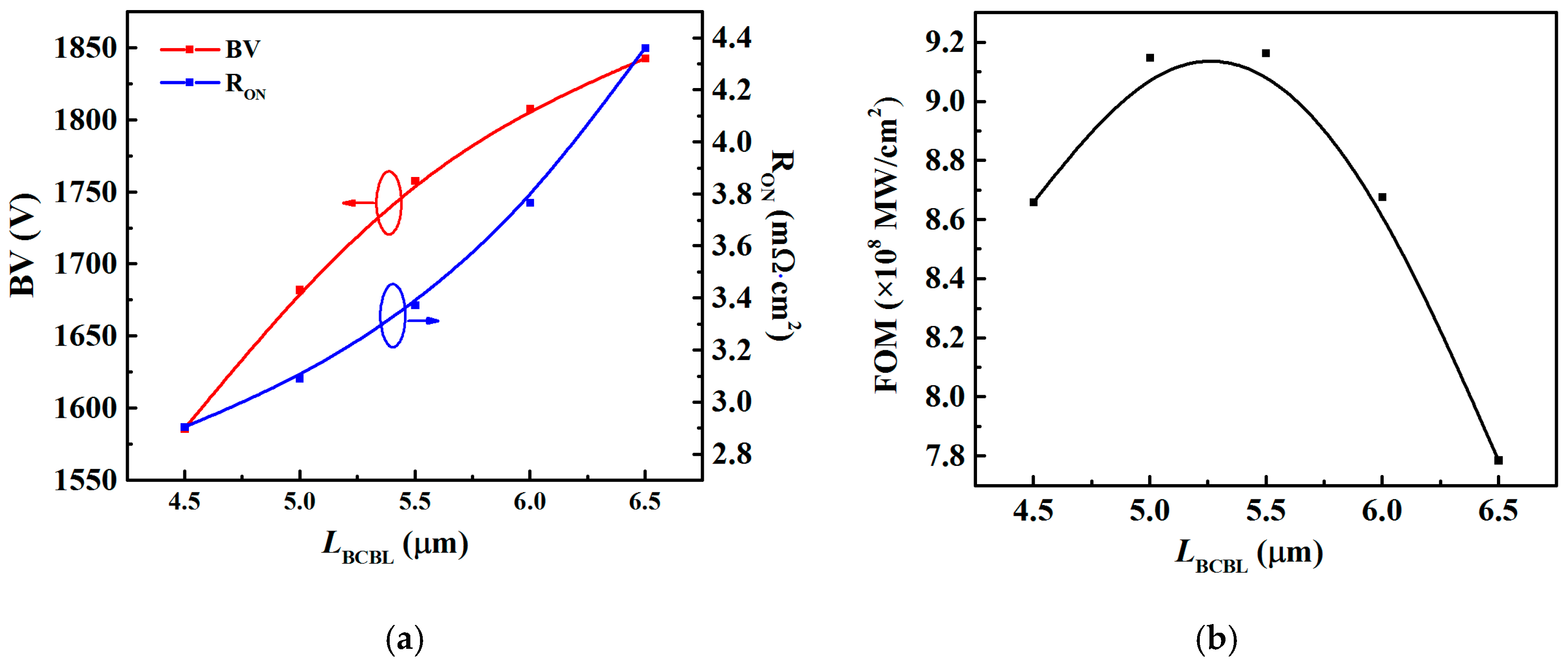
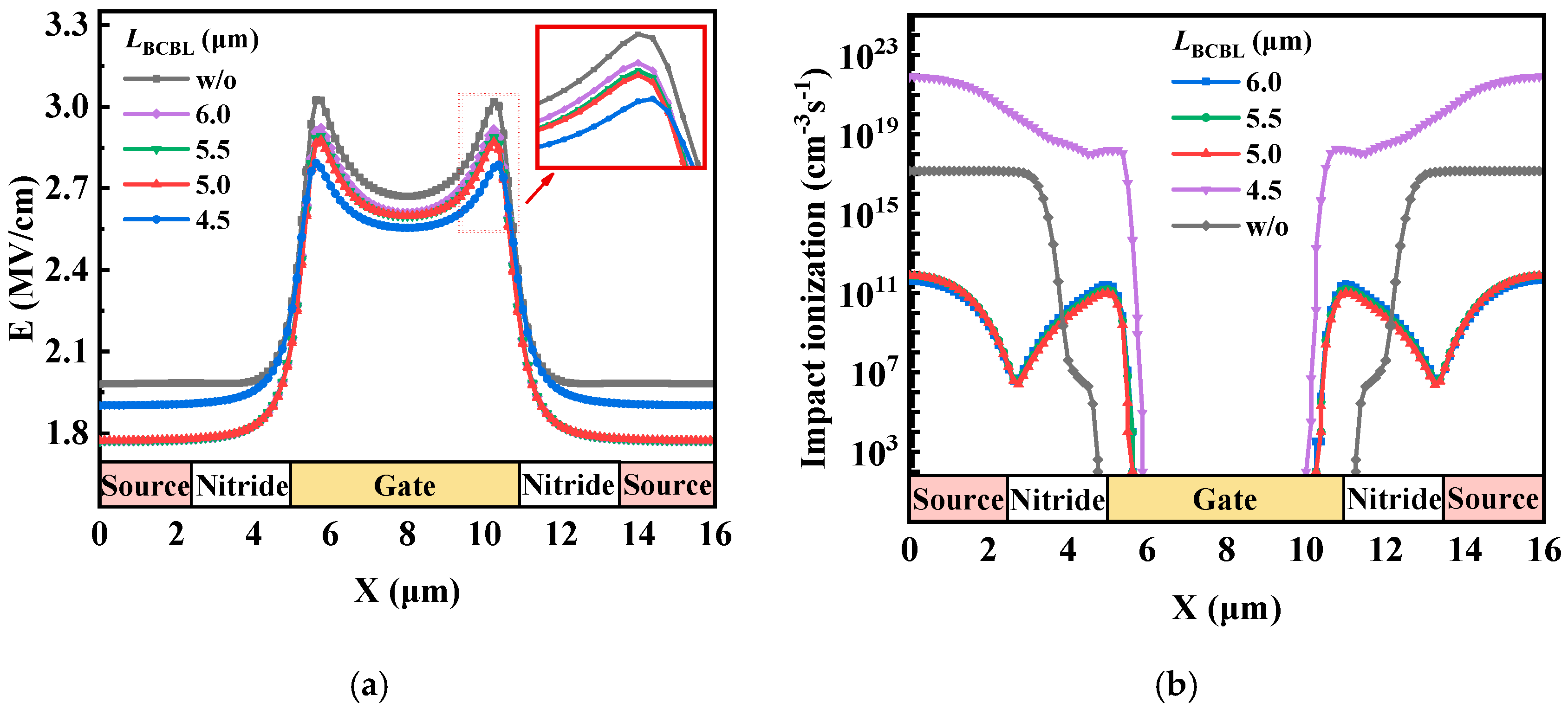
4.1.2. Optimization of LBCBL

The simulated BV and RON data and the calculated FOM values with the changed LBCBL are shown in Figure 6a,b, respectively. Both the BV and RON are increased obviously with the increasing LBCBL mainly due to the narrowing of the vertical current aperture. Figure 6b shows a trade-off between the BV and RON, and then an optimal LBCBL value at around 5.2 μm is determined. Figure 7 shows the distributions of the electric field and impact ionization concentration near the gate in the BCBL-VFET with the changed LBCBL. The additional BCBL shares the voltage drop in the vertical direction which hence improves the BV characteristics of the devices. The average impact ionization concentration in the device with an LBCBL around 5.2 μm is the lowest among all these devices which supports the above conclusions.

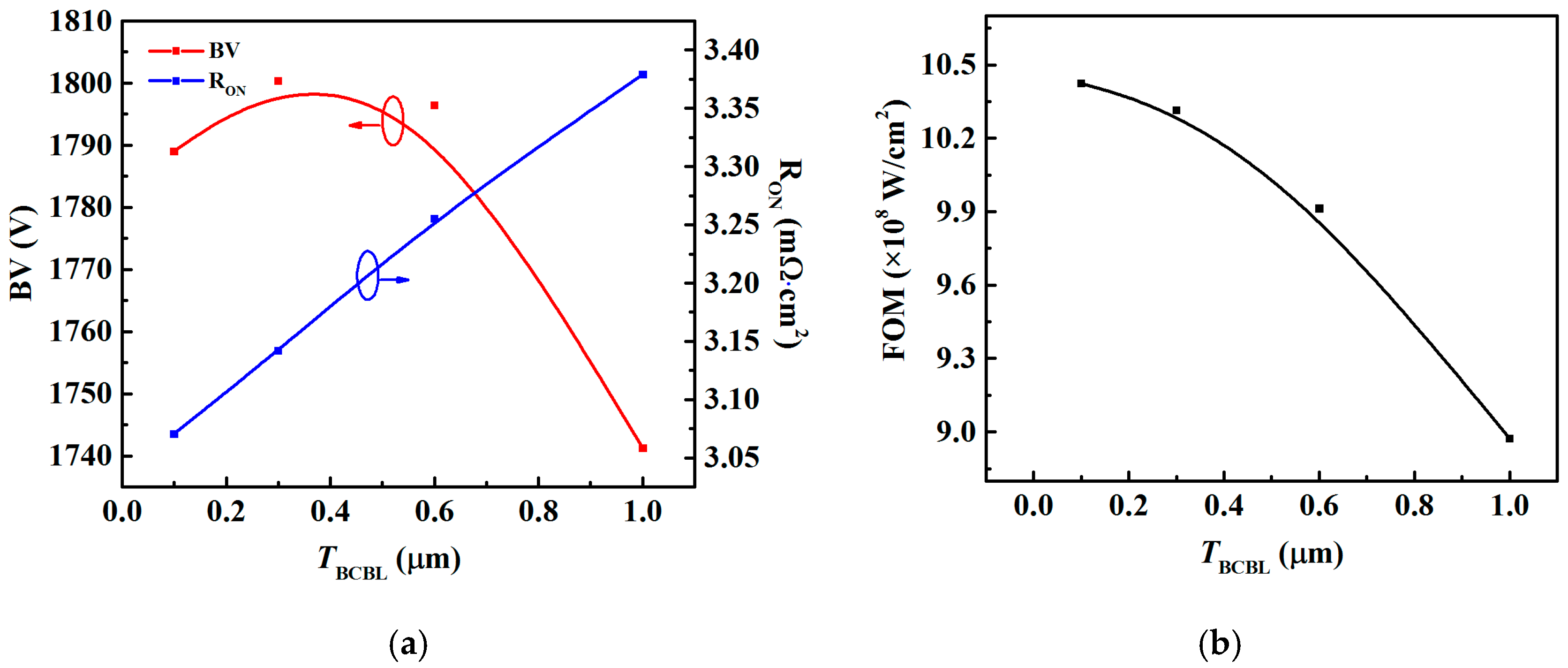
4.1.3. Optimization of TBCBL

The simulated BV and RON data and the calculated FOM values with the changed TBCBL are shown in Figure 8a,b, respectively. The effects of TBCBL variation on both the BV and RON are relatively small. Note that the BV characteristic is improved slightly when the TBCBL increases from 0.1 to 0.4 μm and then the BV decreases; however, the reduction is small and kept within 100 V. Moreover, the RON variations in the proposed devices are also found to be small even though the thickness of the BCBL reaches 1.0 μm. This tells us that a relatively free value of TBCBL can be employed in the BCBL-VFET. This is favorable in the device fabrication. Figure 9a shows the distributions of the electric field around the gate with the changed TBCBL, which are found to be nearly the same among all these devices with a BCBL. However, a different distribution of impact ionization concentration is found in Figure 9b when the thickness of the BCBL reaches 1.0 μm. An additional peak of impact ionization starts to form around the BCBL corner and hence the BV is reduced. Therefore, the TBCBL value should be kept at less than 0.6 μm.

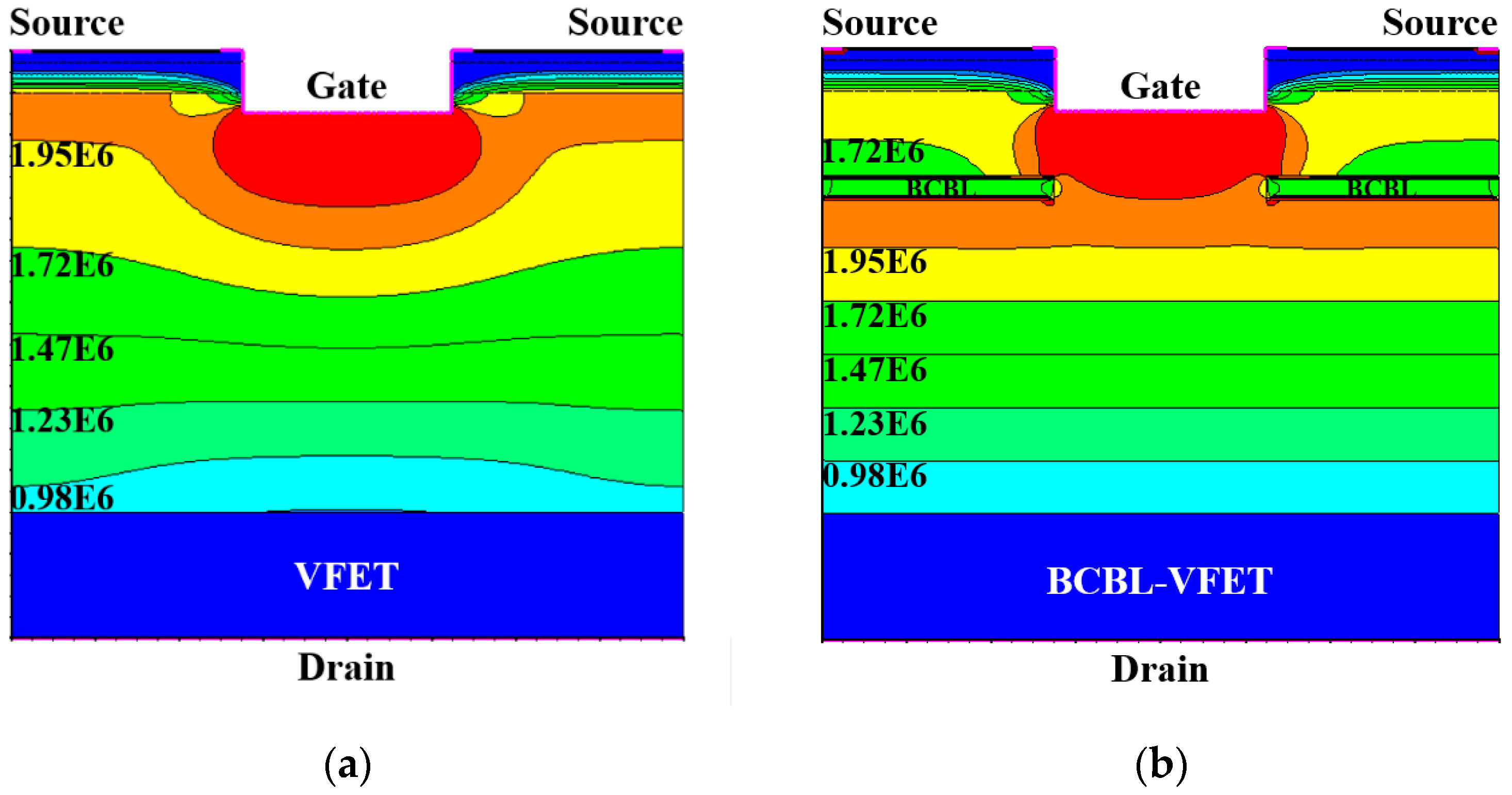
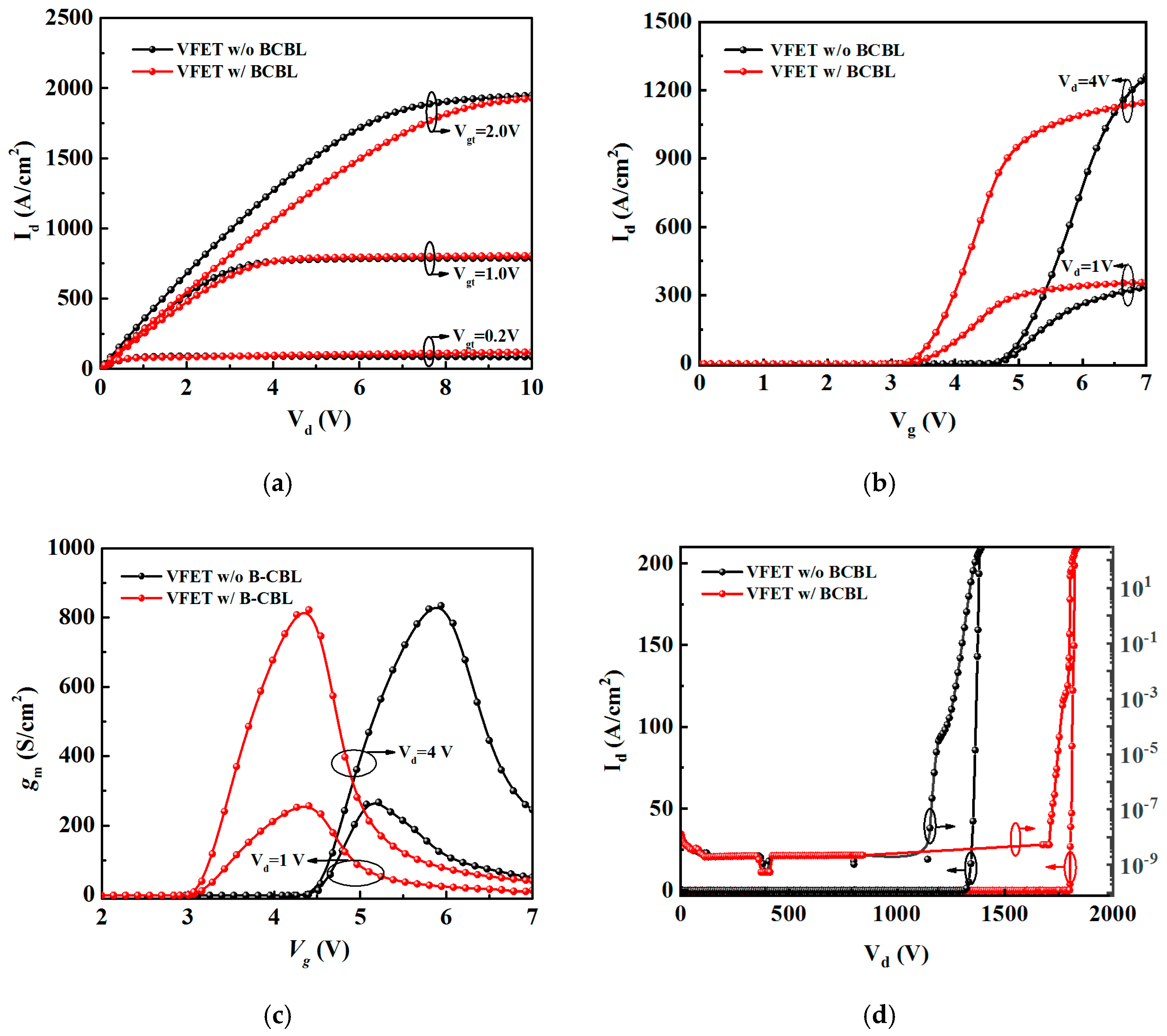
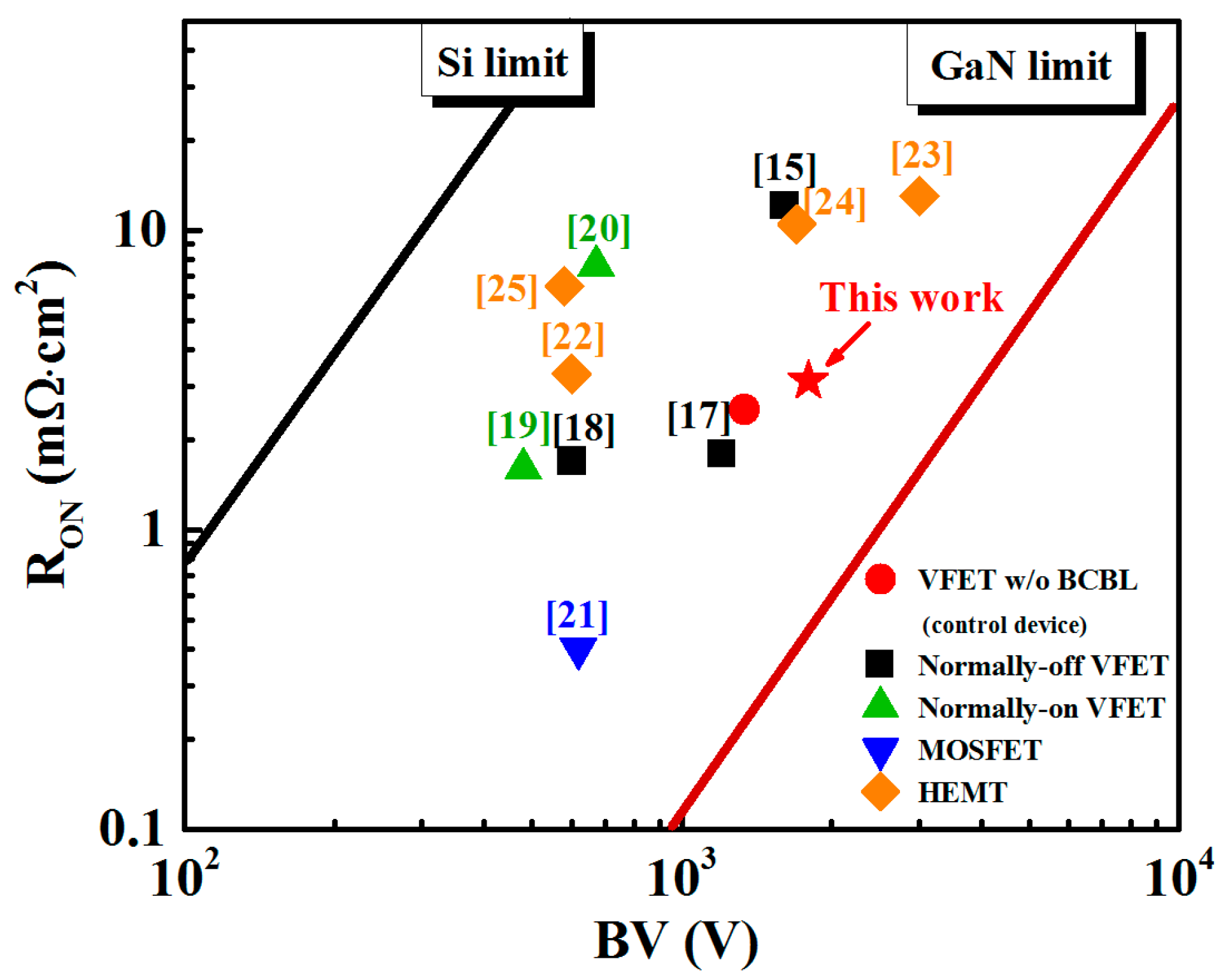
4.2. Performances of the Optimized BCBL-VFET

The optimal parameters of dBCBL, LBCBL, and TBCBL were determined to be 2.0, 5.2, and 0.6 μm, respectively. Figure 10 shows the comparisons of electric field distribution profiles between the optimized BCBL-VFET and the control device. It can be observed that the BCBL can shield the electric field from the pn-junction below the source electrode and hence efficiently protect the TCBL. Furthermore, the electric field distribution is made more uniform and the high-field area around the gate corner is reduced. The output dc Id–Vd, transfer Id–Vg, gate transconductance gm, and BV characteristics of the optimized BCBL-VFET are shown in Figure 11. It can be seen clearly that the normally off operation with a large positive Vth (~3.5 V) is realized in the BCBL-VFET. Only a slight degradation of output Id is found, although the Vth alters by about 1.0 V which might be due to the influence of the BCBL affecting the conducting channel. The degradation of drain current is relatively small at Vgt < 1.5 V and Vd > 8.0 V. To get the optimum performance, the device is recommended to work at about Vgt = 1.5 V and Vd = 10.0 V. The gm peak is around 800 S/cm2 at Vg = 4.5 V and remains nearly the same in comparison to that in the conventional VFET. The large gm value achieved in the BCBL-VFET ensures a high switching frequency of the device. Furthermore, note that the BV of the proposed device is improved significantly compared with the control one.
Figure 12 summarizes the performance comparisons between the proposed BCBL-VFET and other reported GaN-based power devices including VFET, metal-oxide-semiconductor field-effect transistor (MOSFET), and HEMT devices [17,18,19,20,21,22,23,24,25]. It can be seen that the performance of the BCBL-VFET is closer to the GaN limit, compared with the control device and other work. This demonstrates that the proposed scheme would be very promising in the applications of power electronics.
The simulation work is significant and it helps people better understand the physical mechanism in the VFET and save experimental time. The structural parameters are optimized and provided to people for a better device fabrication. However, the actual operating conditions including the operation temperature, switching process, and matching circuit should be also considered seriously for practical applications [26,27,28,29,30]. It is noteworthy that the optimal device structures in this work are based on the dc characteristics. Due to the thermal and trapping effects under actual operating conditions, the dynamic RON and BV can be quite different from the static ones [10,29]. Actually, they are usually worse than the theoretical dc performances, and this needs to be considered in the fabrication work. Nevertheless, the proposed device structure and the optimized results are still constructive and meaningful, and the theoretical trend of device performance changes with the structural parameters should be similar between the dynamic and static ones.
The gm value in the proposed BCBL-VFET is large enough to improve the device switching rate. Since a GaN semiconductor has high electron mobility and saturation rate, the on/off switching speed of the BCBL-VFET should be fast enough after having a stable fabrication technology and a matching gate drive circuit. In this work, the designed BV rating is more than 1800 V which can be applied in an electric vehicle with 600 V rating even taking into account the deviations from the realistic structural parameters and processing technology. Moreover, GaN-based power devices are very promising in the applications in high-temperature environments. The output current–voltage characteristics can remain stable after repeated high-temperature operations. Based on the previous simulation and measurement data [29], only a small Vth deviation of around 0.1 V was found in the metal-insulator-semiconductor (MIS)-gate GaN-based power devices after several rounds of high-temperature measurements from 25 to 150 ℃. More nonlinear dynamic behaviors and actual operating conditions will be considered and taken into account in the following work.

5. Conclusions

A GaN normally off VFET device with an additional BCBL is introduced and demonstrated. The BCBL can lower the peak electric field around the gate and hence make the electric field distribution uniform, which leads to an obvious improvement of the BV characteristics. The structural parameters of the proposed BCBL-VFET have been optimized through theoretical calculations and TCAD simulations. An improved BV of 1800 V and a slightly increased RON of 3.14 mΩ·cm2 are achieved in the BCBL-VFET, compared with 1300 V and 2.52 mΩ·cm2 in the control VFET device. The FOM value of the proposed device can be up to 1.03 GW/cm2, which is 52.5% higher than the control one.

Author Contributions

Writing—Original Draft, F.L.; Methodology, Z.S.; Investigation, N.S. and H.Z.; Software, F.Z.; Data Curation, Y.C.; Validation, P.T.; Writing—Review & Editing, H.H.

Funding

This research was funded by the National Science Foundation of China (grant number 51607022), the Fundamental Research Funds for the Central Universities (grant number DUT17LK13), the Open Project Program of the Key Laboratory of Semiconductor Materials Science (grant number KLSMS-1610), and the Open Project Program of the Key Laboratory of Nanodevices and Applications (grant number 18JG02) from the Chinese Academy of Sciences.

Acknowledgments

The authors are grateful for the support from the Computer Centre of the National University of Singapore.

Conflicts of Interest

The authors declare no conflict of interest.

References

  1. Chen, K.J.; Haberlen, O.; Lidow, A.; Tsai, C.L.; Ueda, T.; Uemoto, Y.; Wu, Y.F. GaN-on-Si Power Technology: Devices and Applications. IEEE Trans. Electron. Devices 2017, 64, 779–795. [Google Scholar] [CrossRef]
  2. Kachi, T. Recent progress of GaN power devices for automotive applications. Jpn. J. Appl. Phys. 2014, 53, 100210. [Google Scholar] [CrossRef] [Green Version]
  3. Ambacher, O.; Foutz, B.; Smart, J.; Shealy, J.R.; Weimann, N.G.; Chu, K.; Murphy, M.; Sierakowski, A.J.; Schaff, W.J.; Eastman, L.F.; et al. Two dimensional electron gases induced by spontaneous and piezoelectric polarization in undoped and doped AlGaN/GaN heterostructures. J. Appl. Phys. 2000, 87, 334–344. [Google Scholar] [CrossRef]
  4. Miao, M.S.; Weber, J.R.; Van de Walle, C.G. Oxidation and the origin of the two-dimensional electron gas in AlGaN/GaN heterostructures. J. Appl. Phys. 2010, 107, 123713. [Google Scholar] [CrossRef]
  5. Oka, T.; Nozawa, T. AlGaN/GaN Recessed MIS-Gate HFET With High-Threshold-Voltage Normally-Off Operation for Power Electronics Applications. IEEE Electron. Device Lett. 2008, 29, 668–670. [Google Scholar] [CrossRef]
  6. Lee, F.; Su, L.; Wang, C.; Wu, Y.; Huang, J. Impact of Gate Metal on the Performance of p-GaN/AlGaN/GaN High Electron Mobility Transistors. IEEE Electron. Device Lett. 2015, 36, 232–234. [Google Scholar] [CrossRef]
  7. Jiang, H.; Tang, C.W.; Lau, K.M. Enhancement-Mode GaN MOS-HEMTs With Recess-Free Barrier Engineering and High-k ZrO2 Gate Dielectric. IEEE Electron. Device Lett. 2018, 39, 405–408. [Google Scholar] [CrossRef]
  8. Dai, S.; Zhou, Y.; Zhong, Y.; Zhang, K.; Zhu, G.; Gao, H.; Sun, Q.; Chen, T.; Yang, H. High fT AlGa(In)N/GaN HEMTs Grown on Si With a Low Gate Leakage and a High ON/OFF Current Ratio. IEEE Electron. Device Lett. 2018, 39, 576–579. [Google Scholar] [CrossRef]
  9. Anderson, T.J.; Tadjer, M.J.; Hite, J.K.; Greenlee, J.D.; Koehler, A.D.; Hobart, K.D.; Kub, F.J. Effect of Reduced Extended Defect Density in MOCVD Grown AlGaN/GaN HEMTs on Native GaN Substrates. IEEE Electron. Device Lett. 2016, 37, 28–30. [Google Scholar] [CrossRef]
  10. Huang, H.L.; Liang, Y.C. Formation of combined partially recessed and multiple fluorinated-dielectric layers gate structures for high threshold voltage GaN-based HEMT power devices. Solid-State Electron. 2015, 114, 148–154. [Google Scholar] [CrossRef]
  11. Ben-Yaacov, I.; Seck, Y.K.; Mishra, U.K.; DenBaars, S.P. AlGaN/GaN current aperture vertical electron transistors with regrown channels. J. Appl. Phys. 2004, 95, 2073–2078. [Google Scholar] [CrossRef]
  12. Kanechika, M.; Sugimoto, M.; Soejima, N.; Ueda, H.; Ishiguro, O.; Kodama, M.; Hnyashi, E.; Itoh, K.; Uesugi, T.; Kachi, T. A vertical insulated gate AlGaN/GaN heterojunction field-effect transistor. Jpn. J. Appl. Phys. 2007, 46, L503–L505. [Google Scholar] [CrossRef]
  13. Ozbek, A.M.; Baliga, B.J. Planar Nearly Ideal Edge-Termination Technique for GaN Devices. IEEE Electron. Device Lett. 2011, 32, 300–302. [Google Scholar] [CrossRef]
  14. Chowdhury, S.; Wong, M.H.; Swenson, B.L.; Mishra, U.K. CAVET on Bulk GaN Substrates Achieved With MBE-Regrown AlGaN/GaN Layers to Suppress Dispersion. IEEE Electron. Device Lett. 2012, 33, 41–43. [Google Scholar] [CrossRef]
  15. Oka, T.; Ueno, Y.; Ina, T.; Hasegawa, K. Vertical GaN-based trench metal oxide semiconductor field-effect transistors on a free-standing GaN substrate with blocking voltage of 1.6 kV. Appl Phys Express 2014, 7, 021002. [Google Scholar] [CrossRef]
  16. Baliga, B.J. Fundamentals of Power Semiconductor Devices; Springer Science & Business Media: Berlin, Germany, 2008; pp. 359–365. [Google Scholar]
  17. Oka, T.; Ina, T.; Ueno, Y.; Nishii, J. 1.8 mΩ·cm2 vertical GaN-based trench metal–oxide–semiconductor field-effect transistors on a free-standing GaN substrate for 1.2-kV-class operation. Appl. Phys. Express 2015, 8, 054101. [Google Scholar] [CrossRef]
  18. Li, R.; Cao, Y.; Chen, M.; Chu, R. 600 V/1.7 Ω Normally-Off GaN Vertical Trench Metal–Oxide–Semiconductor Field-Effect Transistor. IEEE Electron Device Lett. 2016, 37, 1466–1469. [Google Scholar] [CrossRef]
  19. Shrestha, N.M.; Li, Y.M.; Chang, E.Y. Optimal design of the multiple-apertures-GaN-based vertical HEMTs with SiO2 current blocking layer. J. Comput. Electron. 2016, 15, 154–162. [Google Scholar] [CrossRef]
  20. Yaegassi, S.; Okada, M.; Saitou, Y.; Yokoyama, M.; Nakata, K.; Katayama, K.; Ueno, M.; Kiyama, M.; Katsuyama, T.; Nakamura, T. Vertical heterojunction field-effect transistors utilizing re-grown AlGaN/GaN two-dimensional electron gas channels on GaN substrates. Phys. Status Solidi C 2011, 8, 450–452. [Google Scholar] [CrossRef]
  21. Kang, E.G.; Kim, Y.T. Design of Trench Gate GaN Power MOSFET using Al2O3 Gate Oxide. J. Phys. Conf. Ser. 2012, 352, 012025. [Google Scholar] [CrossRef]
  22. Saito, W.; Takada, Y.; Kuraguchi, M.; Tsuda, K.; Omura, I.; Ogura, T. Design and demonstration of high breakdown voltage GaN high electron mobility transistor (HEMT) using field plate structure for power electronics applications. Jpn. J. Appl. Phys. 2004, 43, 2239–2242. [Google Scholar] [CrossRef]
  23. Dogmus, E.; Zegaoui, M.; Medjdoub, F. GaN-on-silicon high-electron-mobility transistor technology with ultra-low leakage up to 3000 V using local substrate removal and AlN ultra-wide bandgap. Appl. Phys. Express 2018, 11, 034102. [Google Scholar] [CrossRef]
  24. Zhao, Z.Q.; Zhao, Z.Y.; Luo, Q.; Du, J.F. High-voltage RESURF AlGaN/GaN high electron mobility transistor with back electrode. Electron. Lett. 2013, 49, 1638–1640. [Google Scholar] [CrossRef]
  25. Huang, H.; Liang, Y.C.; Samudra, G.S.; Ngo, C.L.L. Normally-Off AlGaN/GaN-on-Si MIS-HEMTs Using Combined Partially Recessed and Fluorinated Trap-Charge Gate Structures. IEEE Electron. Device Lett. 2014, 35, 569–571. [Google Scholar] [CrossRef]
  26. Campbell, C.F.; Balistreri, A.; Kao, M.Y.; Dumka, D.C.; Hitt, J. GaN Takes the Lead. IEEE Microw. Mag. 2012, 13, 44–53. [Google Scholar] [CrossRef]
  27. Crupi, G.; Raffo, A.; Avolio, G.; Schreurs, D.M.M.P.; Vannini, G.; Caddemi, A. Temperature Influence on GaN HEMT Equivalent Circuit. IEEE Microw. Wirel. Components 2016, 26, 813–815. [Google Scholar] [CrossRef]
  28. Nalli, A.; Raffo, A.; Crupi, G.; D’Angelo, S.; Resca, D.; Scappaviva, F.; Salvo, G.; Caddemi, A.; Vannini, G. GaN HEMT Noise Model Based on Electromagnetic Simulations. IEEE Trans. Microw. Theory 2015, 63, 2498–2508. [Google Scholar] [CrossRef]
  29. Huang, H.; Li, F.; Sun, Z.; Cao, Y. Model Development for Threshold Voltage Stability Dependent on High Temperature Operations in Wide-Bandgap GaN-Based HEMT Power Devices. Micromachines 2018, 9, 658. [Google Scholar] [CrossRef] [PubMed]
  30. Quaglia, R.; Camarchia, V.; Pirola, M.; Ghione, G. GaN Monolithic Power Amplifiers for Microwave Backhaul Applications. Electronics 2016, 5, 25. [Google Scholar] [CrossRef]
Figure 1. Cross-sectional schematic of the proposed GaN BCBL-VFET (back current blocking layer—vertical field-effect transistor).
Electronics 08 00241 g001
Figure 2. (a) Schematic cross-section, (b) fabrication process flow, (c) top view of the fabricated GaN pn-junction device, and (d) parameter calibration process by benchmarking the simulated I–V characteristics of GaN pn-junction device with the experimental data.
Electronics 08 00241 g002
Figure 3. (a) Breakdown voltage (BV) and on-resistance (RON) versus dBCBL (the distance between the source and the BCBL) and (b) figure of merit (FOM) values versus dBCBL.
Electronics 08 00241 g003
Figure 4. Distributions of (a) electric field and (b) impact ionization concentration near the gate in the BCBL-VFET with the changed dBCBL.
Electronics 08 00241 g004
Figure 5. Schematic view of the equivalent circuit for the overall resistances between source and drain terminals in (a) the conventional vertical field-effect transistor (VFET) and (b) the proposed BCBL-VFET.
Electronics 08 00241 g005
Figure 6. (a) BV and RON versus LBCBL (the length of the BCBL) and (b) FOM values versus LBCBL.
Electronics 08 00241 g006
Figure 7. Distributions of (a) electric field and (b) impact ionization concentration near the gate in the BCBL-VFET with the changed LBCBL.
Electronics 08 00241 g007
Figure 8. (a) BV and RON versus TBCBL (the thickness of the BCBL) and (b) FOM values versus TBCBL.
Electronics 08 00241 g008
Figure 9. Distributions of (a) electric field and (b) impact ionization concentration around the gate in the BCBL-VFET with the changed TBCBL.
Electronics 08 00241 g009
Figure 10. Comparisons of electric field distribution profiles between (a) the conventional VFET and (b) the proposed BCBL-VFET device.
Electronics 08 00241 g010
Figure 11. Comparisons of the typical (a) output dc Id–Vd curves, (b) transfer Id–Vg curves, (c) transconductance gm, and (d) BV characteristics between the proposed BCBL-VFET and conventional VFET devices. For a fair comparison, here Vgt (= Vg – Vth) is employed.
Electronics 08 00241 g011
Figure 12. Performance comparisons among the state-of-the-art GaN-based power devices. The red star represents this work (BCBL-VFET).
Electronics 08 00241 g012
Table 1. Specifics of the proposed GaN BCBL-VFET.
ParametersUnitsValuesParameter Captions
LDμm16.0Drain length
LCAμm5.0Length of vertical current aperture
LGμm5.0Length of the recessed gate
LTOP-CBLμm5.5Length of the top p-GaN
TTOP-CBLμm0.75Thickness of the top p-GaN
TBUFμm10.0Thickness of the buffer layer
Table 2. Physical parameters adopted in the simulations after calibration.
SymbolsUnitsValuesParameter Descriptions
EgeV3.4Band gap of GaN at 300 K
εr--9.4Relative permittivity of GaN
λSeV3.4Affinity of GaN
μncm2/Vs600Electron mobility of GaN
μpcm2/Vs20Hole mobility of GaN
vsatcm/s1.2 × 107Electron saturation velocity of GaN
EmV/cm3.5 × 106Critical electric field of GaN
NCcm−32.2 × 10¹⁸Conduction band state density

