Design of Experiment (DOE) Analysis of System Level ESD Noise Coupling to High-Speed Memory Modules


Abstract
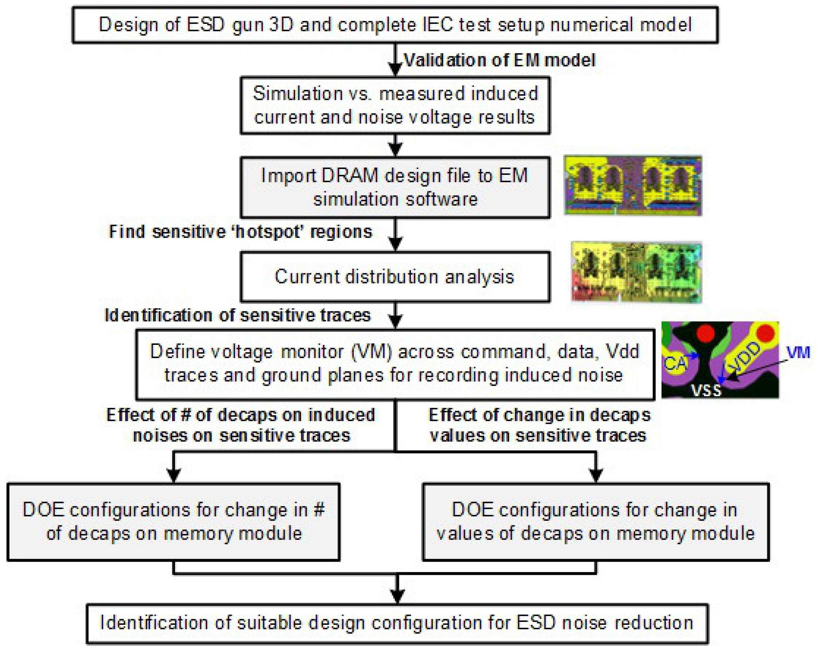
:1. Introduction
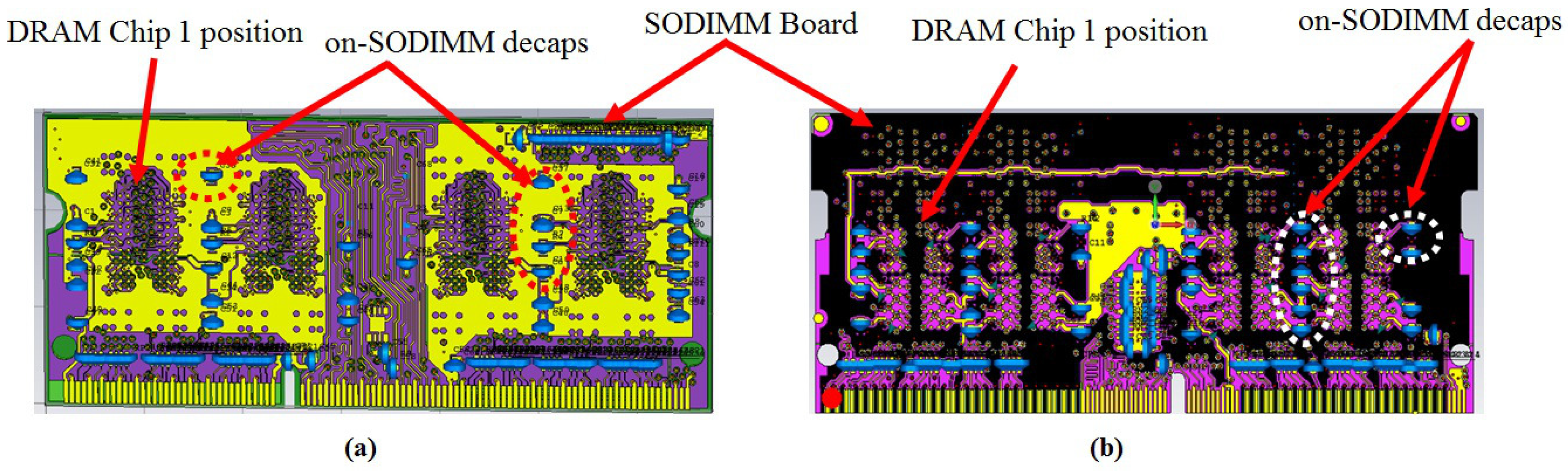
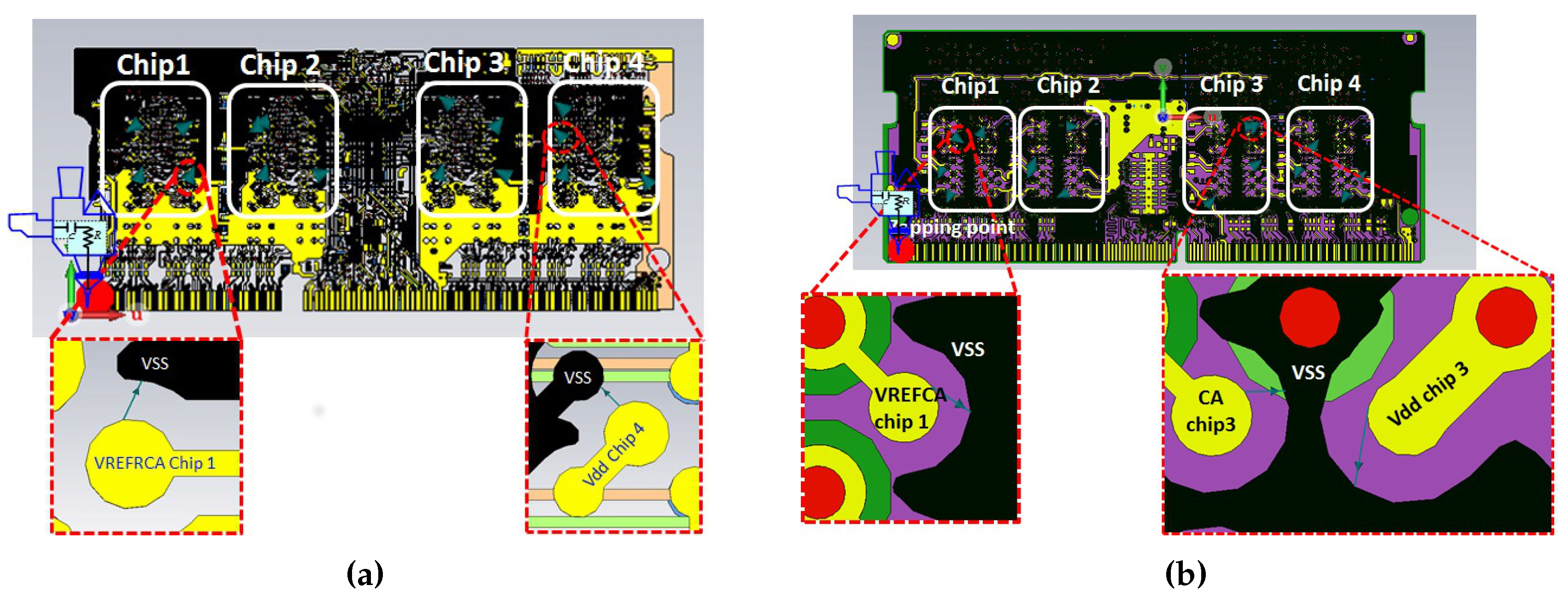
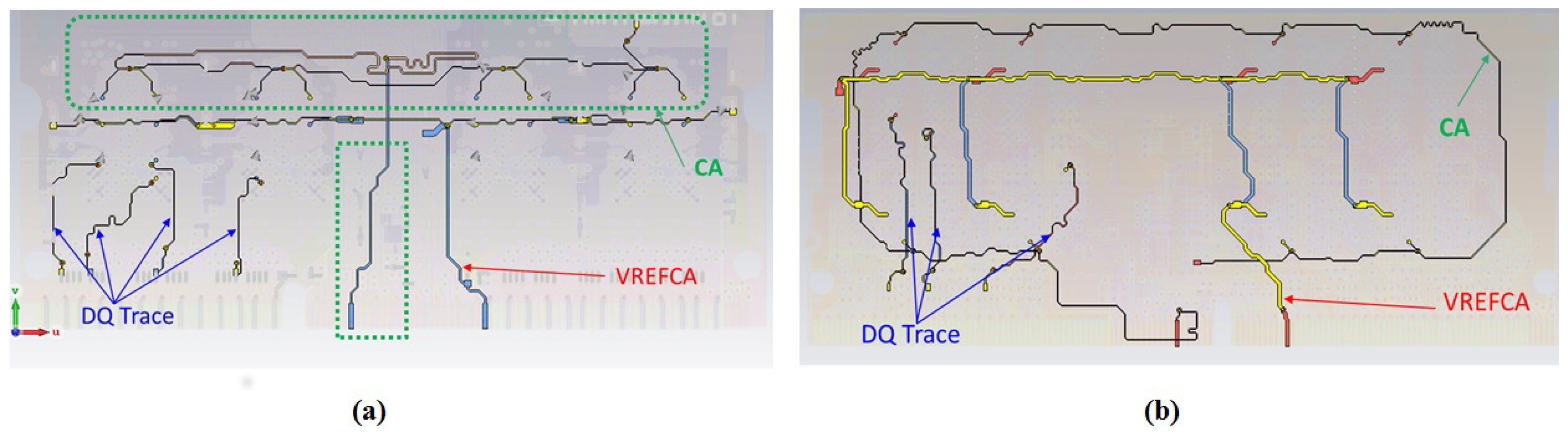
- The sensitive traces on memory modules are identified by monitoring the induced voltages across different nets (by defining the voltage monitors (VM) across the net and ground plane of memory module) around various small outline dual in-line memory module (SODIMM) chips on memory modules
- The effects of the decaps values and number of decaps on induced voltages across identified sensitive traces are analyzed.
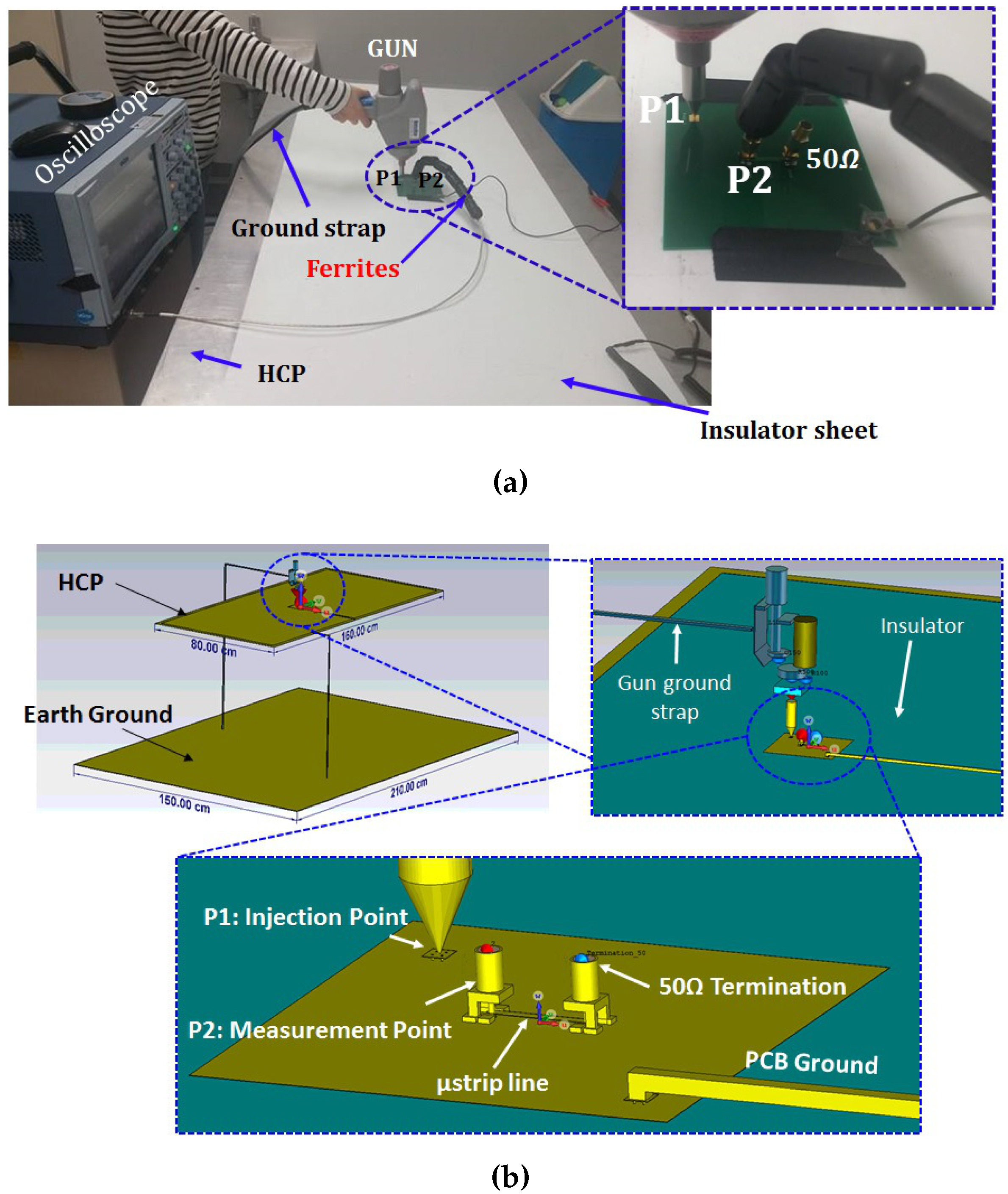
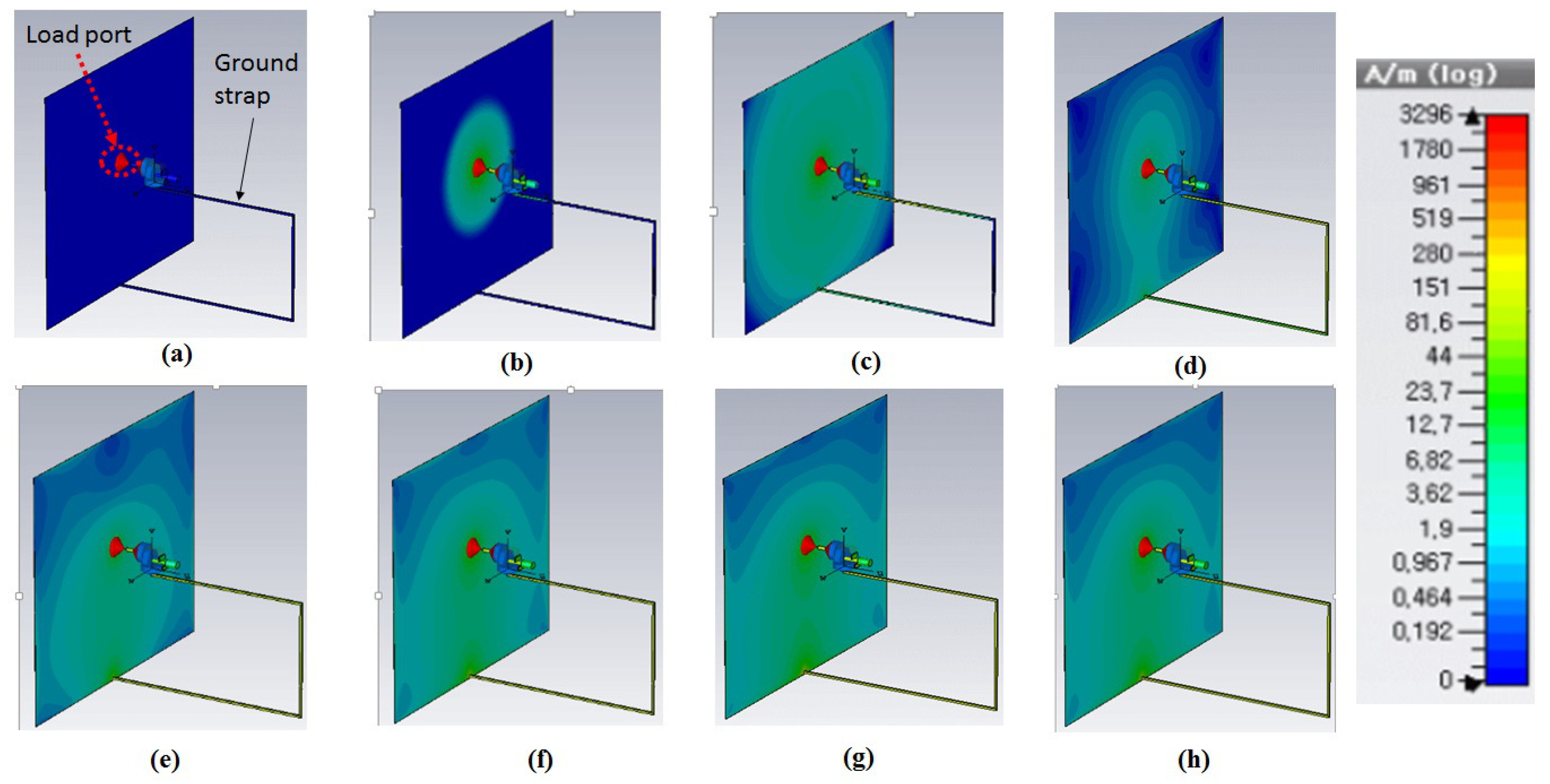
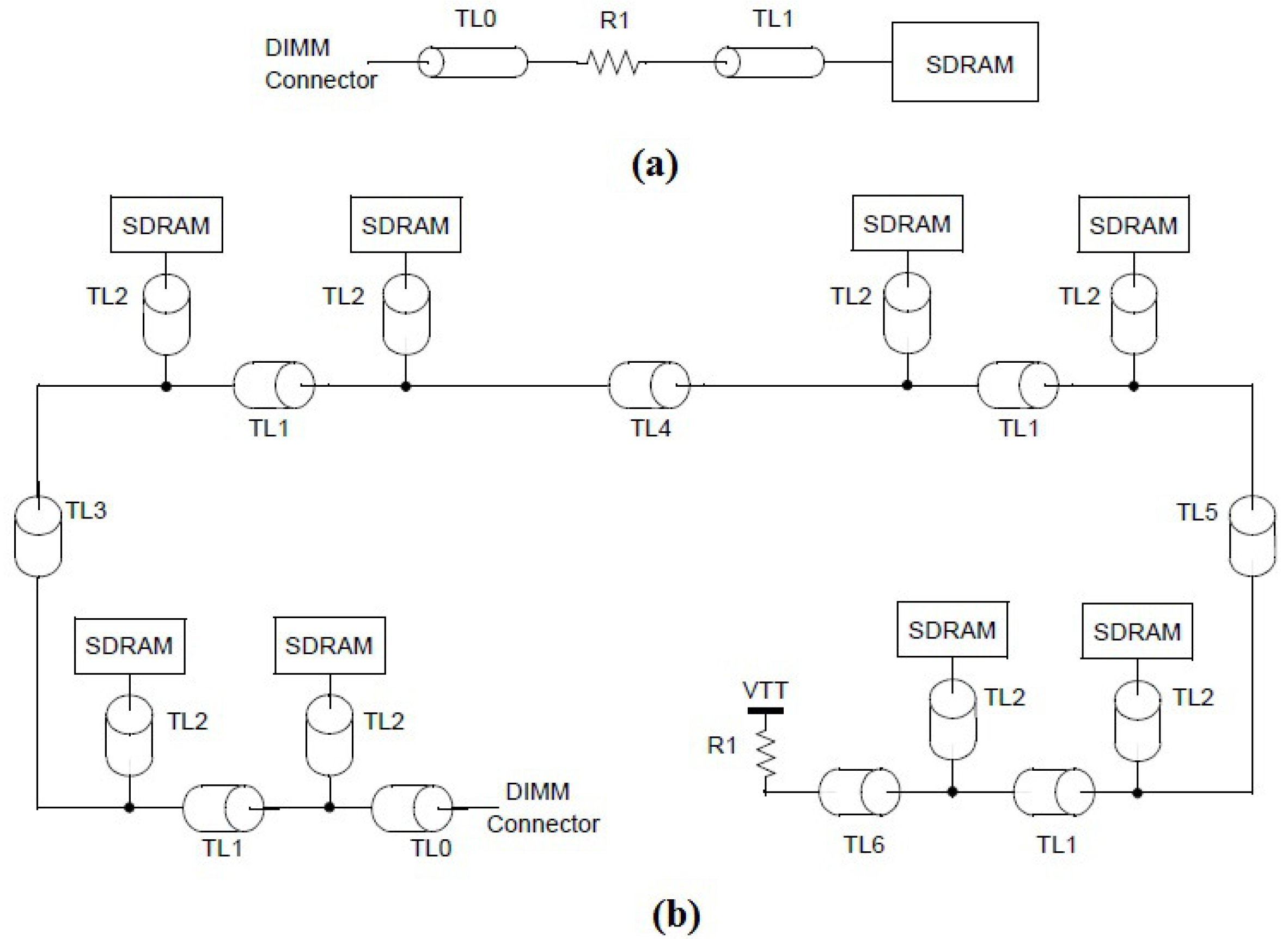
2. Validation of Estimation of Induced ESD Noise Using 3D EM Model
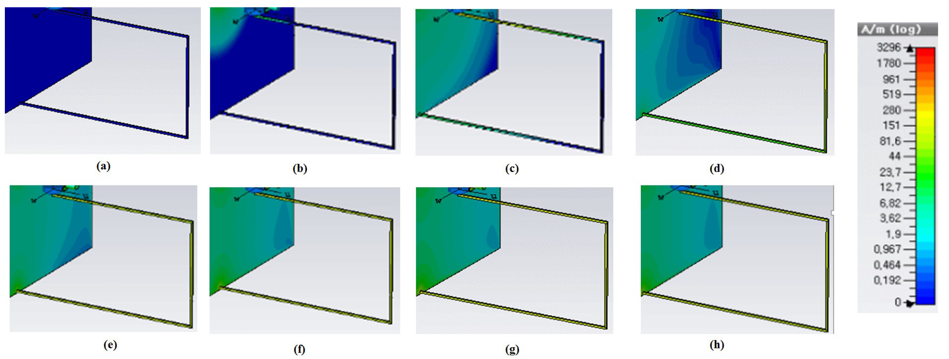
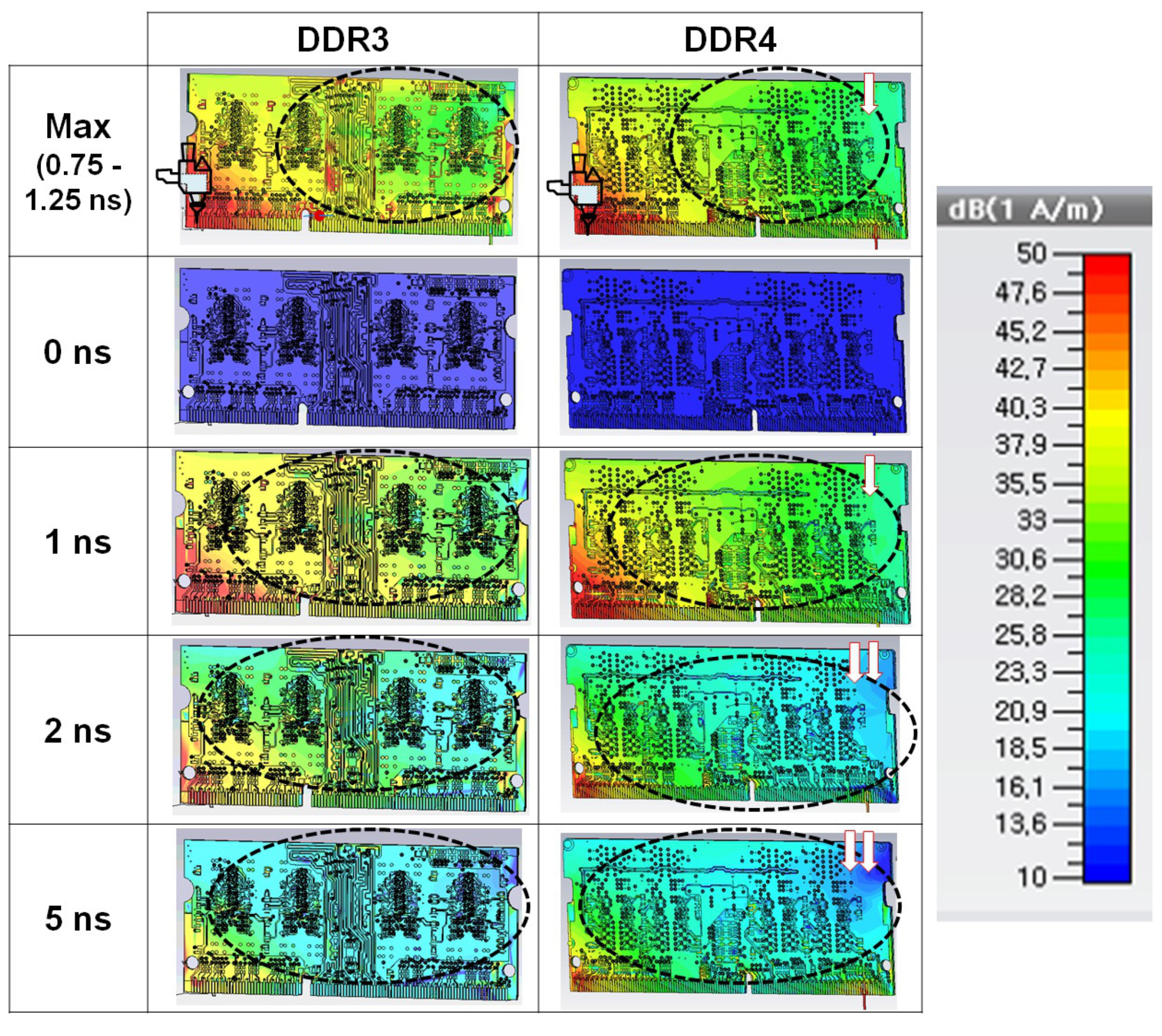
3. Current Distribution Analysis Due to ESD Noise
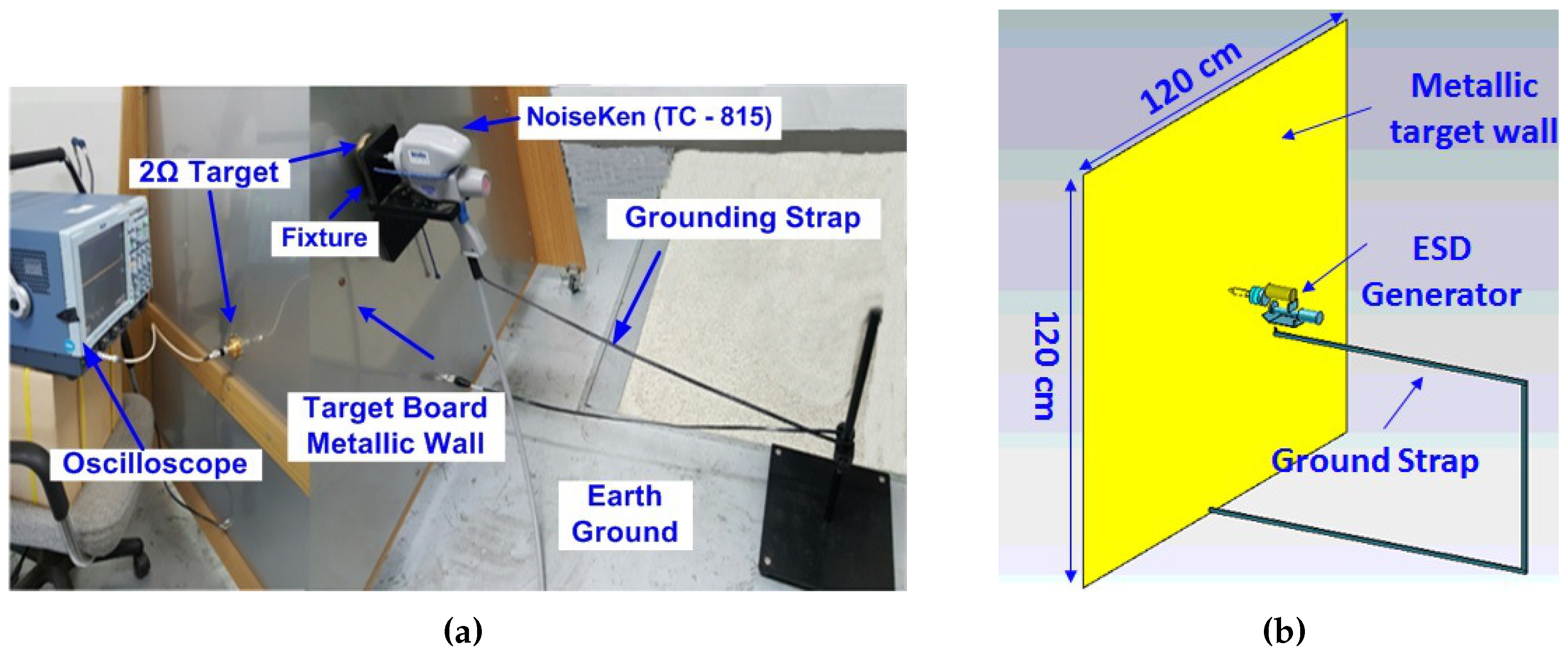
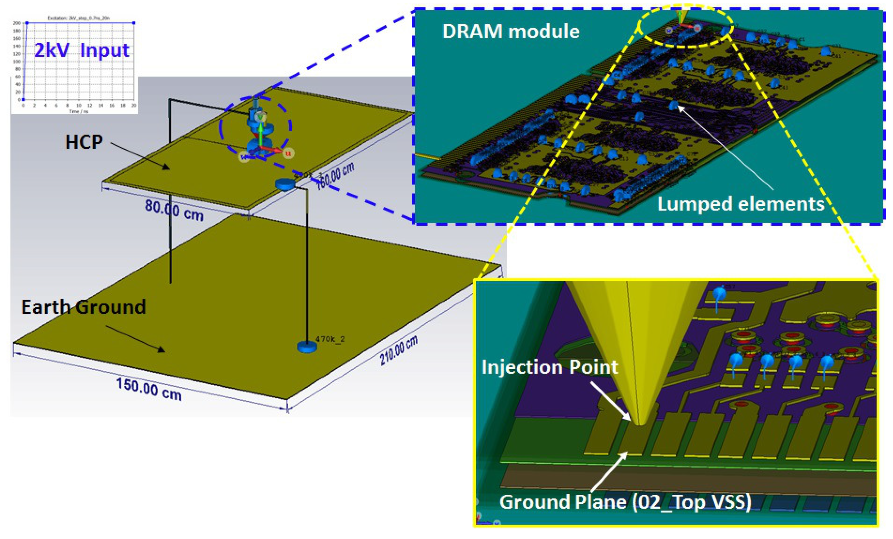
3.1. ESD Gun
3.2. DRAM Memory Modules
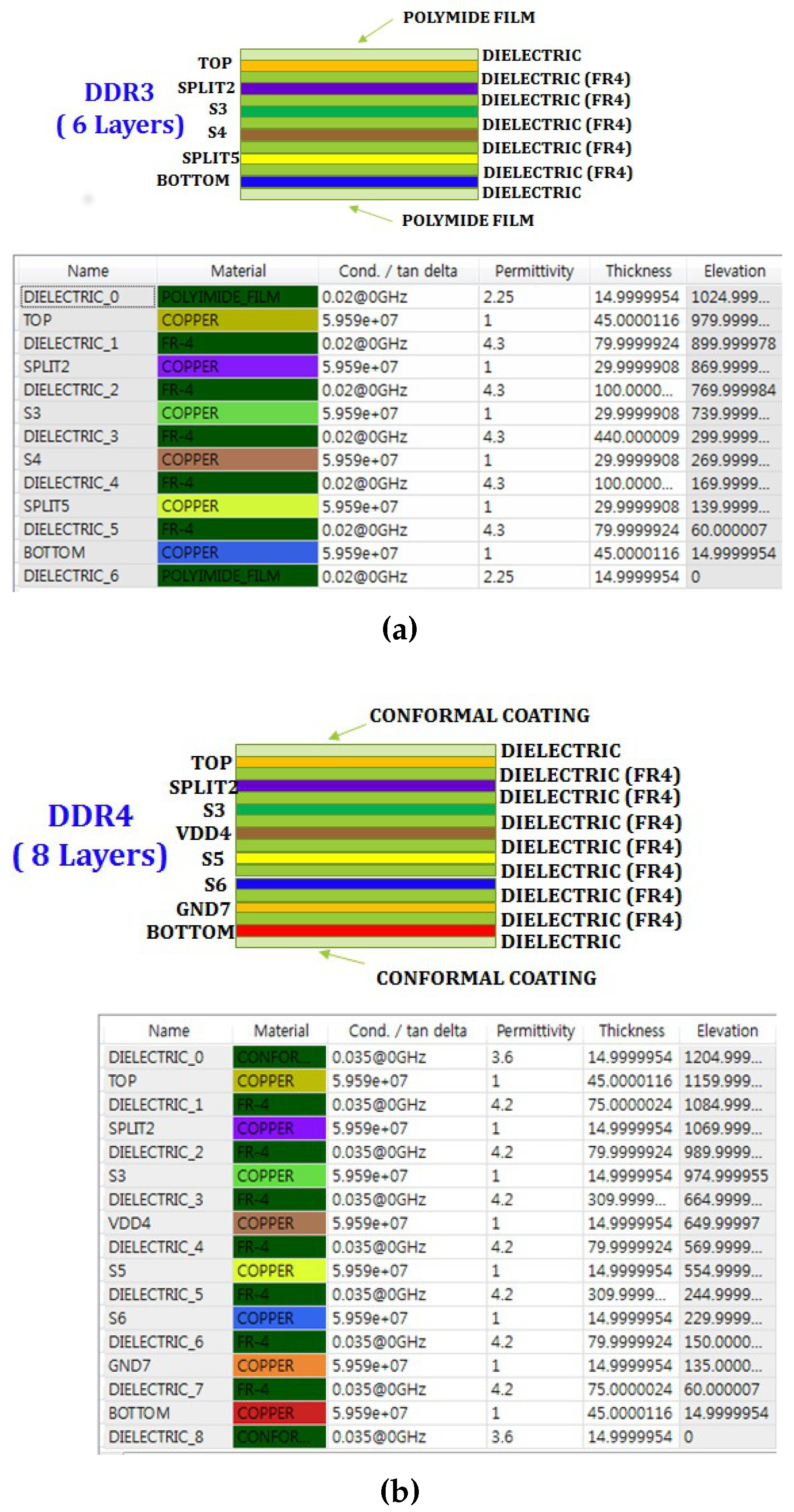
3.2.1. Design Files Importing
3.2.2. Current Distribution Analysis
4. Identification of Sensitive Nets through DOE Analysis
5. Analysis of Effect of Decaps on Coupled Noise on Sensitive Nets through DOE Methodology
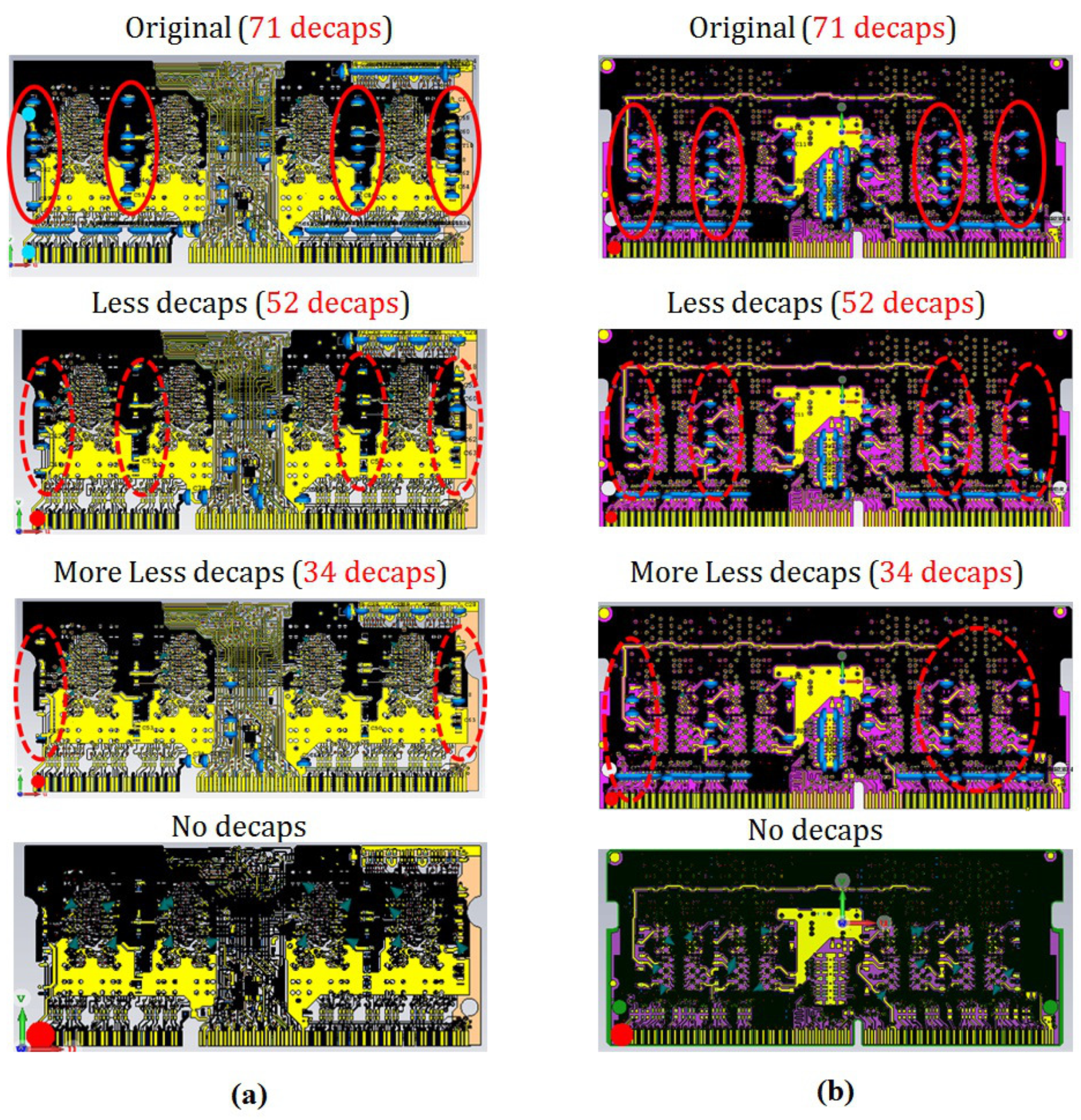
5.1. Effect of Change of Number of Decaps
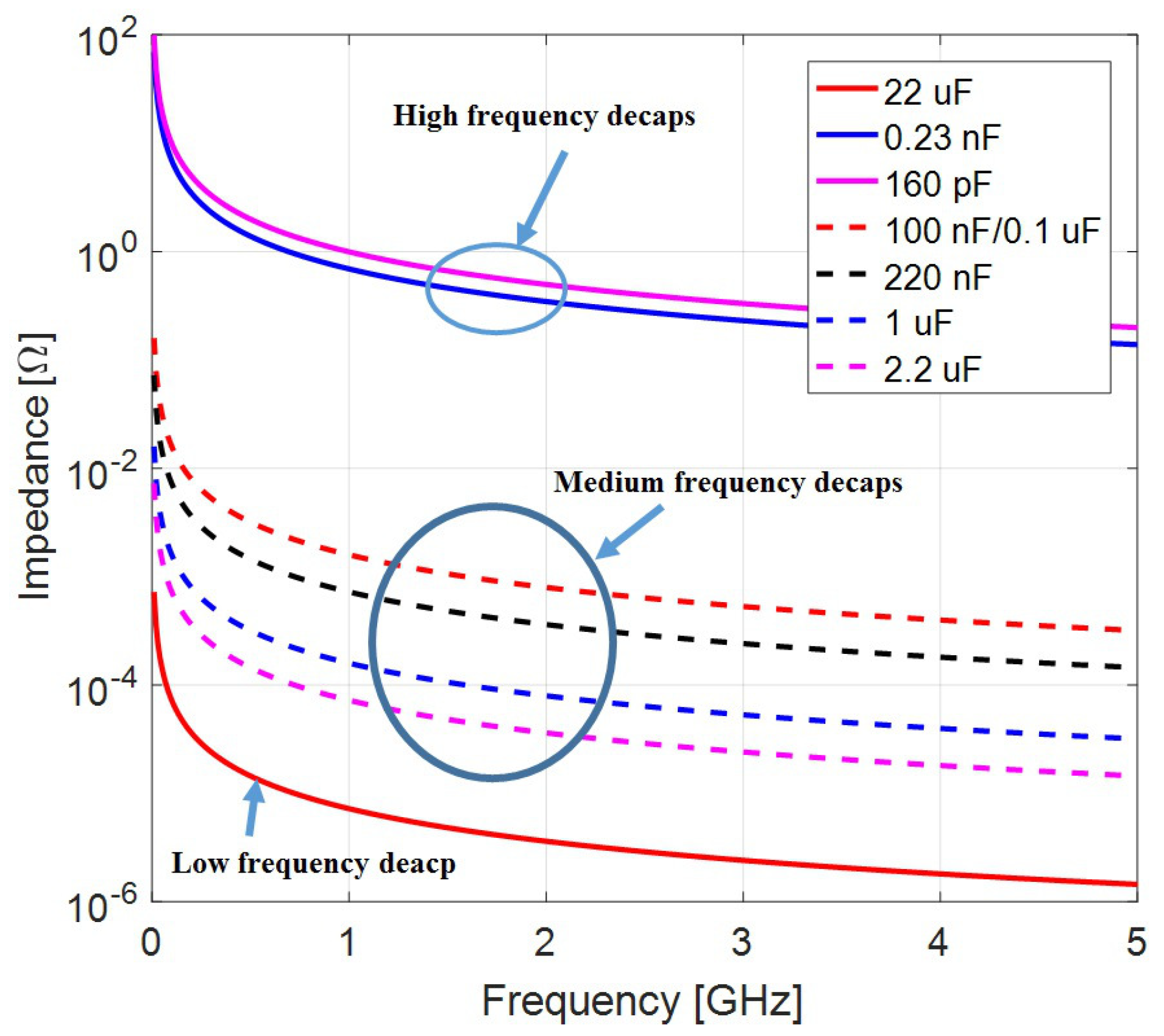
5.2. Effect of Change of Values of Decaps
5.3. Analysis Summary
6. Conclusions
Author Contributions
Funding
Acknowledgments
Conflicts of Interest
Abbreviations
| DOE | Design of experiment |
| ESD | Electrostatic discharge |
| 3D | Three-dimensional |
| HCP | Horizontal coupling plane |
| DRAM | Dynamic random access memory |
| JEDEC | Joint electron device engineering council |
| SODIMM | Small outline dual in-line memory module |
| Decap | Decoupling capacitor |
| MWS | Microwave studio |
| CA | Command address |
| DQ | Data signal |
| GND | Ground |
| VREFCA | Reference voltage for command address |
| OEM | Original equipment manufacturer |
| MLCC | Multi-layer ceramic capacitor |
| MOS | Metal oxide semiconductor |
| EM | Electromagnetic |
| DUT | Device under test |
| IC | Integrated circuit |
| PCB | Printed circuit board |
| VM | Voltage monitor |
| -strip | Microstrip |
| PP | Peak to peak |
| MAX | Maximum |
| ESR | Equivalent series resistance |
| ESL | Equivalent series inductance |
| LF | Low frequency |
| HF | High frequency |
References
- Yousaf, J.; Lee, H.; Nah, W. System Level ESD Analysis-A Comprehensive Review I on ESD Generator Modeling. J. Electr. Eng. Technol. 2018, 13, 2017–2032. [Google Scholar] [CrossRef]
- Yousaf, J.; Lee, H.; Nah, W. System Level ESD Analysis-A Comprehensive Review II on ESD Coupling Analysis Techniques. J. Electr. Eng. Technol. 2018, 13, 2033–2044. [Google Scholar] [CrossRef]
- Koo, J.; Cai, Q.; Wang, K.; Maas, J.; Takahashi, T.; Martwick, A.; Pommerenke, D. Correlation Between EUT Failure Levels and ESD Generator Parameters. IEEE Trans. Electromagn. Compat. 2008, 50, 794–801. [Google Scholar] [CrossRef]
- Fournaris, A.P.; Pocero Fraile, L.; Koufopavlou, O. Exploiting Hardware Vulnerabilities to Attack Embedded System Devices: A Survey of Potent Microarchitectural Attacks. Electronics 2017, 6, 52. [Google Scholar] [CrossRef]
- Muchaidze, G.; Koo, J.; Cai, Q.; Li, T.; Han, L.; Martwick, A.; Wang, K.; Min, J.; Drewniak, J.L.; Pommerenke, D. Susceptibility Scanning as a Failure Analysis Tool for System-Level Electrostatic Discharge (ESD) Problems. IEEE Trans. Electromagn. Compat. 2008, 50, 268–276. [Google Scholar] [CrossRef]
- Kim, K.H.; Kim, Y. Systematic Analysis Methodology for Mobile Phone’s Electrostatic Discharge Soft Failures. IEEE Trans. Electromagn. Compat. 2011, 53, 611–618. [Google Scholar] [CrossRef]
- Baek, S.; Ahn, H.; Ryu, H.; Nam, I.; An, D.; Choi, D.-H.; Byun, M.-S.; Jeong, M.; Kim, B.-E.; Lee, O. A Fully Integrated Dual-Band WLP CMOS Power Amplifier for 802.11n WLAN Applications. J. Electromagn Eng. Sci. 2017, 17, 20–28. [Google Scholar] [CrossRef]
- Lee, Y.S.; Lee, H.-S.; Choi, H.-D. A Study on the Convenient EMF Compliance Assessment for Base Station Installations at a Millimeter Wave Frequency. J. Electromagn Eng. Sci. 2018, 18, 242–247. [Google Scholar] [CrossRef]
- Yousaf, J.; Shin, J.; Leqian, R.; Nah, W.; Youn, J.; Lee, D.; Hwang, C. Effect of ESD generator ground strap configuration on ESD waveform. In Proceedings of the 2017 Asia-Pacific International Symposium on Electromagnetic Compatibility (APEMC), Seoul, Korea, 20–23 June 2017; pp. 121–123. [Google Scholar] [CrossRef]
- Yousaf, J.; Shin, J.; Kim, K.; Youn, J.; Lee, D.; Hwang, C.; Nah, W. System Level ESD Coupling Analysis Using Coupling Transfer Impedance Function. IEEE Trans. Electromagn. Compat. 2018, 60, 310–321. [Google Scholar] [CrossRef]
- Yousaf, J.; Lee, H.; Park, M.; Nah, W.; Youn, J.; Lee, D.; Hwang, C. Efficient analysis of ESD noise coupling to mobile device memory module. In Proceedings of the 2018 IEEE International Symposium on Electromagnetic Compatibility and 2018 IEEE Asia-Pacific Symposium on Electromagnetic Compatibility (EMC/APEMC), Singapore, 14–18 May 2018; pp. 1198–1202. [Google Scholar] [CrossRef]
- Yousaf, J.; Han, J.; Lee, H.; Nah, W.; Youn, J.; Mun, S.; Lee, D.; Hwang, C. Fast Characterization of System Level ESD Noise Coupling to Real Motherboard in Notebook. In Proceedings of the 2018 International Symposium on Electromagnetic Compatibility (EMC EUROPE), Amsterdam, The Netherlands, 27–30 August 2018; pp. 957–962. [Google Scholar] [CrossRef]
- Koo, J.; Cai, Q.; Muchaidze, G.; Martwick, A.; Wang, K.; Pommerenke, D. Frequency-Domain Measurement Method for the Analysis of ESD Generators and Coupling. IEEE Trans. Electromagn. Compat. 2007, 49, 504–511. [Google Scholar] [CrossRef]
- Park, M.; Park, J.; Choi, J.; Kim, J.; Jeong, S.; Seung, M.; Lee, S.; Kim, J. Measurement and Analysis of Statistical IC Operation Errors in a Memory Module Due to System-Level ESD Noise. IEEE Trans. Electromagn. Compat. 2018, 1–11. [Google Scholar] [CrossRef]
- Xiao, J.; Pommerenke, D.; Drewniak, J.L.; Shumiya, H.; Maeshima, J.; Yamada, T.; Araki, K. Model of Secondary ESD for a Portable Electronic Product. IEEE Trans. Electromagn. Compat. 2012, 54, 546–555. [Google Scholar] [CrossRef]
- Liu, D.; Nandy, A.; Pommerenke, D.; Kwon, S.J.; Kim, K.H. Full wave model for simulating a Noiseken ESD generator. In Proceedings of the 2009 IEEE International Symposium on Electromagnetic Compatibility, Austin, TX, USA, 17–21 August 2009; pp. 334–339. [Google Scholar] [CrossRef]
- Qing, C.; Koo, J.; Nandy, A.; Pommerenke, D.; Lee, J.S.; Seol, B.S. Advanced full wave ESD generator model for system level coupling simulation. In Proceedings of the 2008 IEEE International Symposium on Electromagnetic Compatibility, Detroit, MI, USA, 18–22 August 2008; pp. 1–6. [Google Scholar] [CrossRef]
- Caniggia, S.; Maradei, F. Numerical Prediction and Measurement of ESD Radiated Fields by Free-Space Field Sensors. IEEE Trans. Electromagn. Compat. 2007, 49, 494–503. [Google Scholar] [CrossRef]
- Yousaf, J.; Park, M.; Lee, H.; Youn, J.; Lee, D.; Hwang, C.; Nah, W. Efficient Circuit and an EM Model of an Electrostatic Discharge Generator. IEEE Trans. Electromagn. Compat. 2018, 60, 1078–1086. [Google Scholar] [CrossRef]
- Jiya, I.N.; Gurusinghe, N.; Gouws, R. Electrical Circuit Modelling of Double Layer Capacitors for Power Electronics and Energy Storage Applications: A Review. Electronics 2018, 7, 268. [Google Scholar] [CrossRef]
- Lee, J.S.; Pommerenke, D.; Lim, J.D.; Seol, B. ESD field coupling study in relation with PCB GND and metal chassis. In Proceedings of the 2009 20th International Zurich Symposium on Electromagnetic Compatibility, Zurich, Switzerland, 12–16 January 2009; pp. 153–156. [Google Scholar] [CrossRef]
- Yousaf, J.; Shin, J.; Lee, H.; Nah, W.; Youn, J.; Lee, D.; Hwang, C. Efficient circuit and EM model of electrostatic discharge generator. In Proceedings of the 2017 IEEE International Symposium on Electromagnetic Compatibility Signal/Power Integrity (EMCSI), Washington, DC, USA, 7–11 August 2017; pp. 164–168. [Google Scholar] [CrossRef]
- Electromagnetic Compatibility (EMC)-Part 4-2: Testing and Measurement Techniques Electrostatic Discharge (ESD) Immunity Test; IEC 61000-4-2: 2008; Technical Report for IEC: Piscataway, NJ, USA, 2008.
- PC3-14900/PC3L-12800 SO-DIMM. Available online: https://www.jedec.org/content/pc3-14900pc3l-12800-so-dimm (accessed on 2 March 2018).
- PC4-2133 Unbuffered SODIMM. Available online: https://www.jedec.org/content/pc4-2133-unbuffered-sodimm-0 (accessed on 2 March 2018).
- Kim, D.; Rieh, J.-S. Comparison of Two Layout Options for 110-GHz CMOS LC Cross-Coupled Oscillators. J. Electromagn Eng. Sci. 2018, 18, 141–143. [Google Scholar] [CrossRef]
- Lee, I.; Kim, J.; Jeon, S. A G-Band Frequency Doubler Using a Commercial 150 nm GaAs pHEMT Technology. J. Electromagn Eng. Sci. 2017, 17, 147–152. [Google Scholar] [CrossRef]
- Meng, X.; Saleh, R. An Improved Active Decoupling Capacitor for ’Hot-Spot’ Supply Noise Reduction in ASIC Designs. IEEE J. Solid-State Circuits 2009, 44, 584–593. [Google Scholar] [CrossRef]
- Park, J.; Kim, J.; Lee, J.; Jo, C.; Seol, B. System-level ESD noise induced by secondary discharges at voltage suppressor devices in a mobile product. In Proceedings of the 2017 Asia-Pacific International Symposium on Electromagnetic Compatibility (APEMC), Seoul, Korea, 20–23 June 2017; pp. 70–72. [Google Scholar] [CrossRef]
- Lin, S.W.; Chen, S.C. Predicting the Yield Rate of DRAM Modules by Support Vector Regression. In Global Perspective for Competitive Enterprise, Economy and Ecology; Springer: London, UK, 2009; pp. 747–755. [Google Scholar]


| DDR3 | DDR4 | |
|---|---|---|
| Memory standard | JEDEC | JEDEC |
| DIMM version | 204-pin Unbuffered SODIMMs | 260-pin Unbuffered SODIMMs |
| Title | PC3-SODIMM_V210_RC_B4_20111220 | PC4-SODIMM_V090_RC_A0_20131025 |
| Raw card revision | B4 | A0 |
| Reference Specification | DDR3 Unbuffered SODIMM Reference Design Standard Rev. 2.1 | DDR4 SO-DIMM Design Specification Annex-A0 Item 2228.08 |
| DDR3 | DDR4 | ||
|---|---|---|---|
| Configuration | 1R × 8 SODIMM | 1R × 8 SODIMM | |
| # of layers | 6 | 8 | |
| BOM | R | 15 × 24 ea 30 × 2 ea 36 × 9 ea 75 × 1 ea 240 × 8 ea | 15 × 37 ea 36 × 2 ea 39 × 7 ea 51 × 1 ea 75 × 1 ea 120 × 1 ea 240 × 8 ea |
| Total R | 44 | 57 | |
| C | 1 × 5 ea 2.2 × 4 ea 100 × 52 ea 220 × 9 ea 3.3 × 1 ea | 0.01 × 1 ea 0.1 × 9 ea 1 × 61 ea 100 × 1 ea 3.3 × 1 ea | |
| Total C | 71 | 73 | |
| Chip 1 | Chip 2 | Chip 3 | Chip 4 | |||||
|---|---|---|---|---|---|---|---|---|
| Trace | Max [V] | PP [V] | Max [V] | PP [V] | Max [V] | PP [V] | Max [V] | PP [V] |
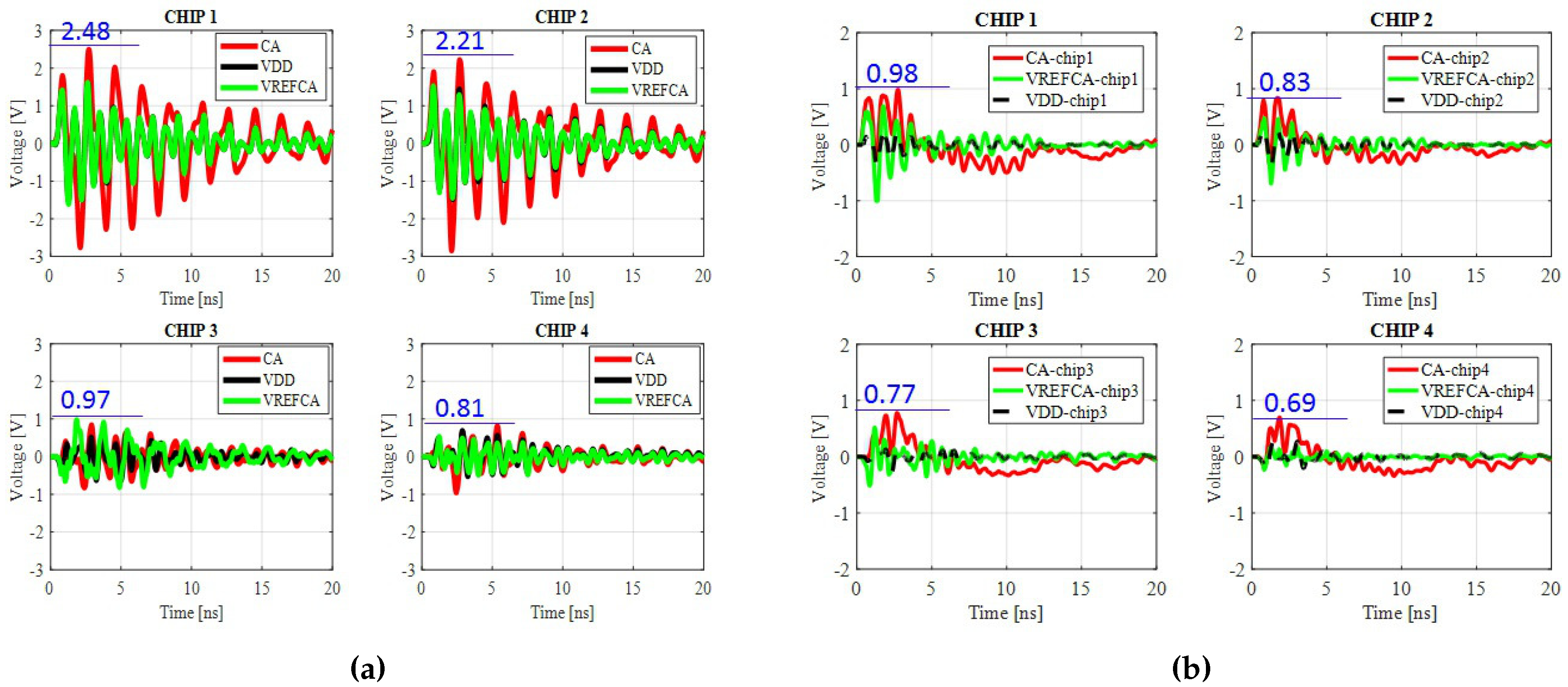
| CA | 2.48 | 5.25 | 2.21 | 5.06 | 0.83 | 1.66 | 0.81 | 1.77 |
| VREFCA | 1.61 | 3.22 | 1.52 | 2.97 | 0.97 | 1.78 | 0.53 | 1.01 |
| VDD | 1.60 | 3.13 | 1.48 | 2.96 | 0.61 | 1.23 | 0.68 | 1.21 |
| Chip 1 | Chip 2 | Chip 3 | Chip 4 | |||||
|---|---|---|---|---|---|---|---|---|
| Trace | Max [V] | PP [V] | Max [V] | PP [V] | Max [V] | PP [V] | Max [V] | PP [V] |
| CA | 0.98 | 1.49 | 0.83 | 1.20 | 0.77 | 1.10 | 0.69 | 1.03 |
| VREFCA | 0.68 | 1.69 | 0.68 | 1.69 | 0.51 | 1.03 | 0.17 | 0.40 |
| VDD | 0.29 | 0.65 | 0.47 | 1.17 | 0.14 | 0.41 | 0.26 | 0.48 |
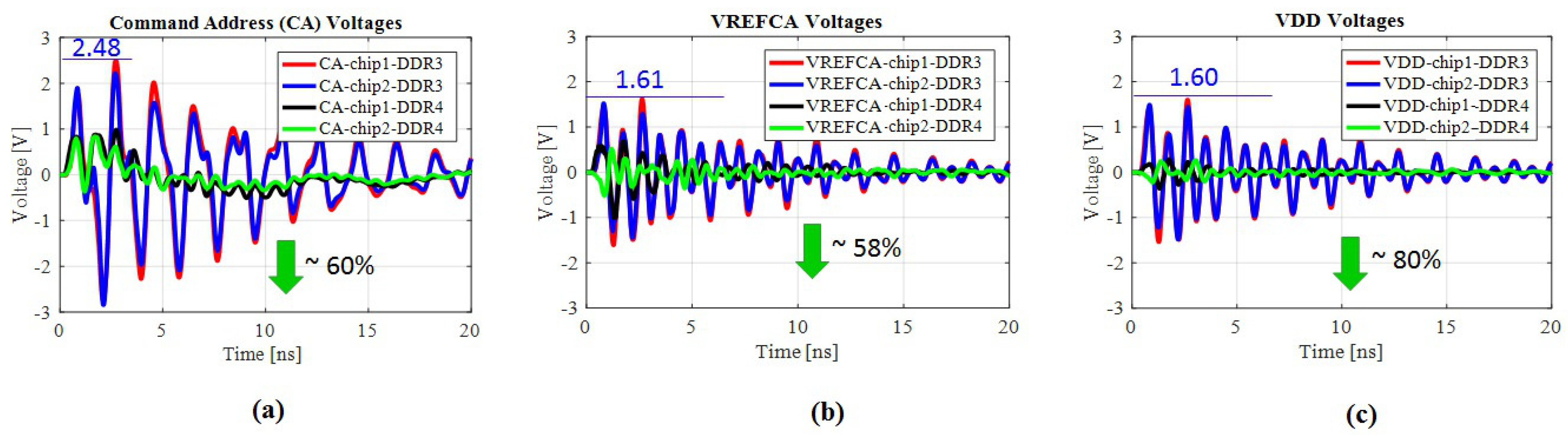
| Trace | CA-Chip 1 | CA-Chip 2 | VREFCA-Chip 1 | VREFCA-Chip 2 | VDD-Chip 1 | VDD-Chip 2 |
|---|---|---|---|---|---|---|
| DDR3 | 2.48 | 2.21 | 1.61 | 1.52 | 1.60 | 1.48 |
| DDR4 | 0.98 | 0.83 | 0.68 | 0.68 | 0.29 | 0.47 |
| Reduction in DDR4 (%) | −60 | −62 | −58 | −55 | −82 | −68 |
| Installed Decaps | ||
|---|---|---|
| Connection Planes | DDR3 | DDR4 |
| VREFCA-VDD | 100 × 9 ea | 0.1 × 8 ea |
| VREFDQ-VSS | 100 × 9 ea | - |
| VDD-VSS(GND) | 100 × 18 ea 220 × 9 ea 1 × 5 ea 2.2 × 4 ea | 1 × 31 ea |
| VTT-VDD | 100 × 14 ea | 1 × 14 ea |
| VPP-GND | - | 1 × 16 ea |
| Case | 1 | 2 | 3 | 4 |
|---|---|---|---|---|
| DUT | DDR3 | |||
| Case Description | Original Decaps (71) | Less decaps (52) | More less decaps (34) | No deacp |
| DUT | DDR4 | |||
| Case Description | Original Decaps (73) | Less decaps (52) | More less decaps (34) | No deacp |
| Case # | 1 | 2 | 3 | 4 | ||||
|---|---|---|---|---|---|---|---|---|
| DUT | DDR3 | |||||||
| Trace | Max [V] | PP [V] | Max [V] | PP [V] | Max [V] | PP [V] | Max [V] | PP [V] |
| CA | 2.48 | 5.25 | 2.90 | 6.22 | 5.63 | 11.1 | 15.73 | 23.33 |
| VREFCA | 1.61 | 3.13 | 2.43 | 5.33 | 5.48 | 11 | 17.55 | 26.1 |
| VDD | 1.60 | 3.22 | 2.54 | 5.46 | 6.51 | 12.7 | 13.1 | 19.3 |
| DUT | DDR4 | |||||||
| CA | 0.98 | 1.49 | 1.45 | 2.17 | 1.74 | 2.67 | 2.57 | 3.64 |
| VREFCA | 0.68 | 1.69 | 1.07 | 2.70 | 1.50 | 3.31 | 2.54 | 3.85 |
| VDD | 0.29 | 0.65 | 0.37 | 0.84 | 0.49 | 1.12 | 0.71 | 1.53 |
| Connection Planes | VRREFCA-VDD | VREFDQ-VSS | VDD-VSS (GND) | VTT-VDD | VPP-GND | Total # of Changed Values Decaps |
|---|---|---|---|---|---|---|
| DUT | DDR3 | |||||
| Case 1 (Original configuration) | 100 × 9 | 100 × 9 | 100 × 18 220 × 9 1 × 5 2.2 × 4 | 100 × 14 | - | |
| Case 5 (# of changed values decaps) | 100 → 0.23 (9) | 100 → 160 (9) | 100 → 160 (13) 220 → 160 (6) 1 → 160 (5) | NC | - | 42 |
| Case 6 (# of changed values decaps) | 100 → 22 (9) | 100 → 22 (9) | 100 → 22 (13) 220 → 22 (6) 1 → 22 (5) | NC | - | 42 |
| Case 7 (# of changed values decaps) | 100 → 0.23 (5) | 100 → 160 (5) | 100 → 160 (12) | NC | - | 22 |
| DUT | DDR4 | |||||
| Case 1 (Original configuration) | 0.1 × 8 | - | 1 × 31 | 1 × 14 | 1 × 16 | - |
| Case 5 (# of changed values decaps) | 0.1 → 160 (8) | - | 1 → 160 (31) | NC | NC | 39 |
| Case 6 (# of changed values decaps) | 0.1 → 22 (8) | - | 1 → 22 (31) | NC | NC | 39 |
| Case 7 (# of changed values decaps) | 0.1 → 160 (4) | - | 1 → 160 (14) | NC | NC | 18 |
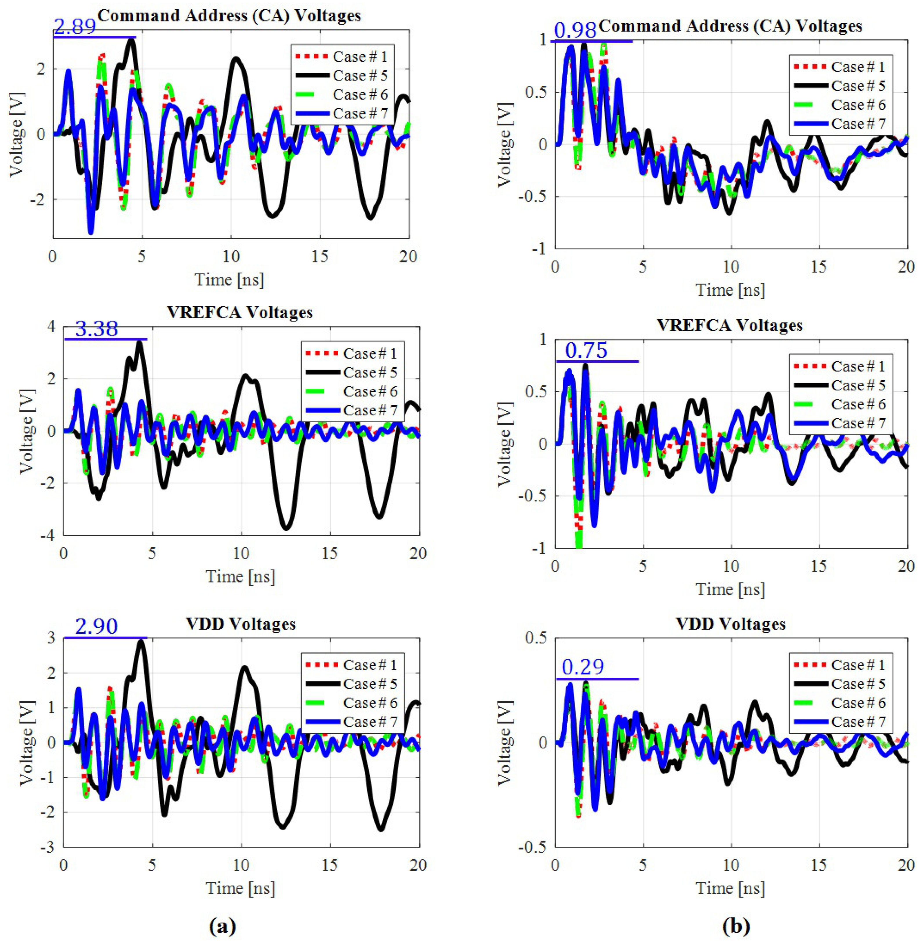
| Case | 1 | 5 | 6 | 7 | ||||
|---|---|---|---|---|---|---|---|---|
| DUT | DDR3 | |||||||
| Trace | Max [V] | PP [V] | Max [V] | PP [V] | Max [V] | PP [V] | Max [V] | PP [V] |
| CA | 2.48 | 5.25 | 2.89 | 5.47 | 2.48 | 5.25 | 1.94 | 4.96 |
| VREFCA | 1.60 | 3.13 | 3.38 | 7.12 | 1.61 | 3.22 | 1.56 | 3.16 |
| VDD | 1.61 | 3.22 | 2.90 | 5.40 | 1.60 | 3.13 | 1.53 | 3.14 |
| DUT | DDR4 | |||||||
| CA | 0.98 | 1.49 | 0.96 | 1.61 | 0.96 | 1.46 | 0.93 | 1.52 |
| VREFCA | 0.68 | 1.69 | 0.75 | 1.41 | 0.68 | 1.69 | 0.70 | 1.48 |
| VDD | 0.29 | 0.65 | 0.28 | 0.57 | 0.27 | 0.62 | 0.27 | 0.59 |
© 2019 by the authors. Licensee MDPI, Basel, Switzerland. This article is an open access article distributed under the terms and conditions of the Creative Commons Attribution (CC BY) license (http://creativecommons.org/licenses/by/4.0/).
Share and Cite
Yousaf, J.; Faisal, M.; Youn, J.; Nah, W. Design of Experiment (DOE) Analysis of System Level ESD Noise Coupling to High-Speed Memory Modules. Electronics 2019, 8, 210. https://doi.org/10.3390/electronics8020210
Yousaf J, Faisal M, Youn J, Nah W. Design of Experiment (DOE) Analysis of System Level ESD Noise Coupling to High-Speed Memory Modules. Electronics. 2019; 8(2):210. https://doi.org/10.3390/electronics8020210
Chicago/Turabian StyleYousaf, Jawad, Muhammad Faisal, Jinsung Youn, and Wansoo Nah. 2019. "Design of Experiment (DOE) Analysis of System Level ESD Noise Coupling to High-Speed Memory Modules" Electronics 8, no. 2: 210. https://doi.org/10.3390/electronics8020210
APA StyleYousaf, J., Faisal, M., Youn, J., & Nah, W. (2019). Design of Experiment (DOE) Analysis of System Level ESD Noise Coupling to High-Speed Memory Modules. Electronics, 8(2), 210. https://doi.org/10.3390/electronics8020210