A Low-Power Spike-Like Neural Network Design


Abstract
1. Introduction
- A fully customizable hardware design for a SNN-like neural network. A software application automatically generates the hardware code for the integration of all neurons in the network. In addition, comparisons with a standard multiply-and-add NN version are provided;
- Use of duty-cycle encoding for the signals between neurons. This allows for efficient routing and for hardware usage minimization;
- Implementation of thrifting, i.e., limiting the number of inputs for a neuron. This was first tested in software and then validated on the hardware architecture;
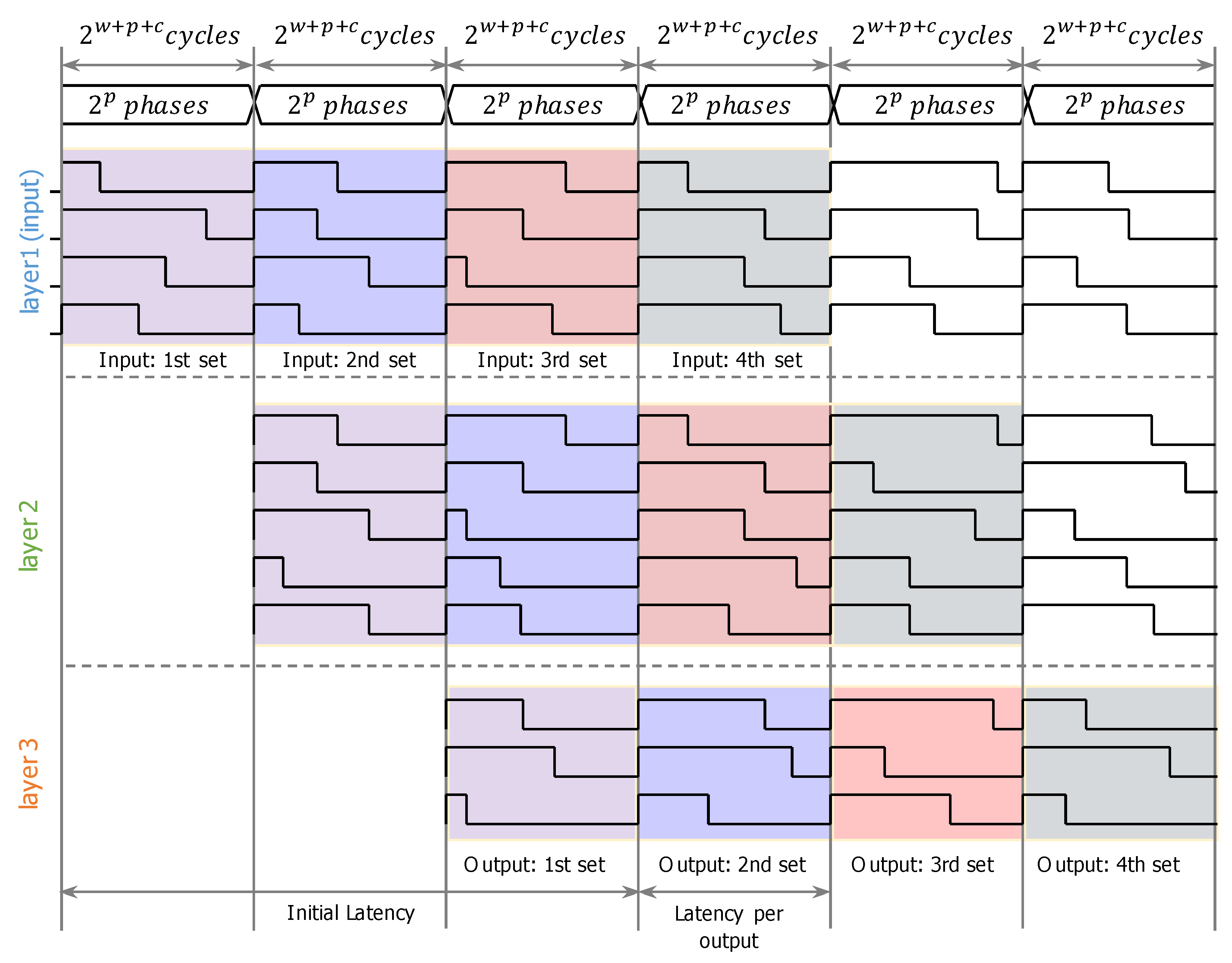
- Pipelined neural network: Each layer is always processing data. Output results are generated as one set per frame, where a frame is defined as the processing time of a layer. The frame time only depends on the hardware parameters, and not on the data;
- A bit-serial neuron design that only requires a counter, 1-bit multiplexors, and comparators.
2. Background
2.1. Artificial Neural Network Fundamentals
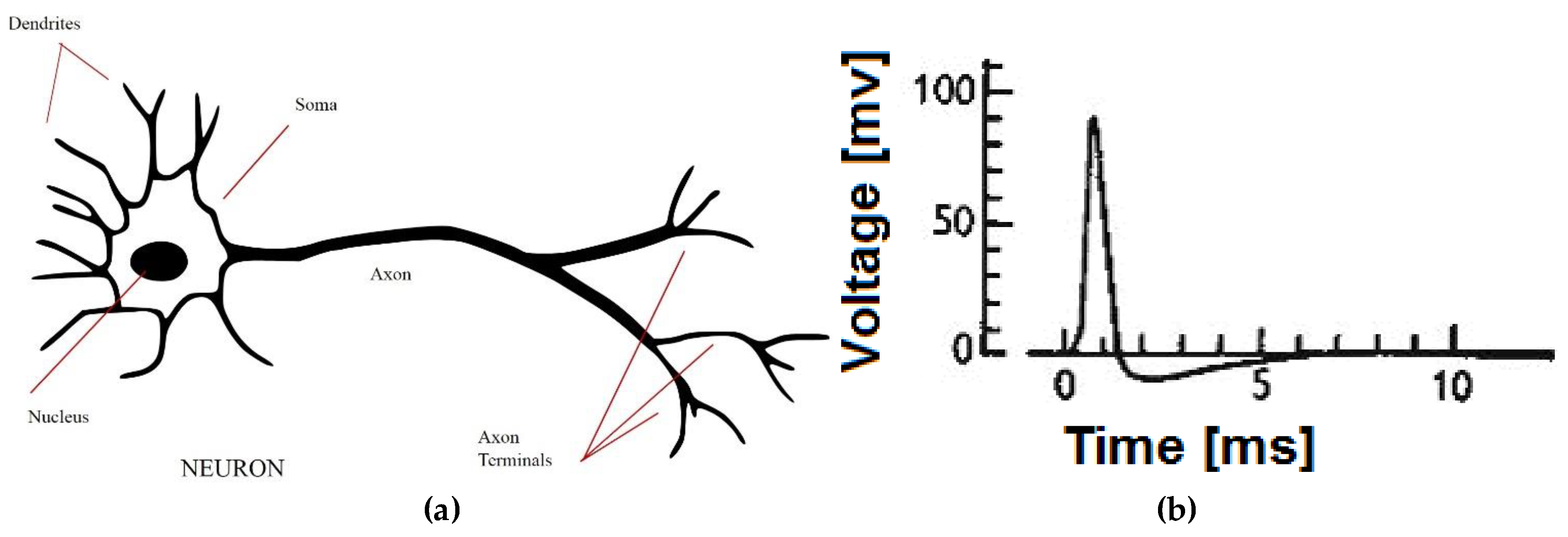
2.2. Spiking Neural Networks
- The output of a given unit can be represented by a single wire rather than by an 8-bit or 16-bit bus. This simplifies routing in the FPGA and reduces the size of registers and other elements;
- Spikes (as pulses) can be easily counted (up/down counter), making the integration a straightforward process rather than utilizing multi-bit accumulators;
- Weights (gain factors) for input connections can be realized by repeated sampling of the input pulse as per the gain level or by ‘step counting’ after receiving each input pulse;
- In the analog domain, specially-designed transistors may be used to better implement the integrate and fire behavior with very few active components by using a special charge-accumulating semiconductor layer. Also, analog signals are more robust to modest amounts of signal pulse collision (two signals hit the bus at the same time), within the limits of saturation.
- However, there exist some challenges to applying SNNs in applications, such as:
- Many existing processors, input, and output devices are designed to work with multi-bit digitized signals. Spike-oriented encoding methods are uncommon among current electronics components and system designs, although there are some examples of duty-cycle encoding (variable pulse width for a set pulse frequency) or pulse-rate encoding. Pure analog-domain transducers exist, and components such as voltage-controlled oscillators (VCOs) may be a useful front-end interface. If SNNs become more prominent, interfacing mechanisms will improve;
- If spikes are represented by 1-bit pulses, if two of more outputs feeding a single input are firing at the same time, it will be received as a single spike pulse, and any multiplicity of spikes will be lost. For a large and robust enough network, the signal loss due to spike collision may not impact the accuracy significantly. This collision effect can be minimized if the pulses are kept short and each unit producing an output delays the timing of the output by a variable amount within a longer time window. This delay could be random, pre-configured to avoid conflict with other units, or externally-triggered and coordinated to minimize conflict. Alternatively, the multiple output spikes can be held over a longer period so the receiving unit may sample each one using a series of sub-spike sampling period. These techniques, however, introduce latency;
- Some types of neural network layers, such as the softmax layer that emphasizes one output among a set of outputs (the best classification out of multiple possibilities) and normalizes them in a likelihood-based ration, are difficult to implement in a SNN. It is possible to make do without such layers, but interpretation of SNN output becomes somewhat less intelligible;
- Perhaps the most fundamental challenge is that training of SNNs is not as straightforward as the conventional ANNs. Back-propagation of network error compared to the expected results is a gradient descent operation where the local slope of an error surface is expected to be smooth due to differentiability of the neuron internal operation. Depending on the SNN design, there may be internal variables that provide a smooth error surface for gradient descent. Alternatively, we can train an ANN proxy of the intended SNN with gradient descent and map the gain and bias values to the SNN representation with reasonable overall performance. We also note that there are training approaches unique to SNNs such as Spike-Timing-Dependent Plasticity (STDP) that reinforces connections in the network where the input spike is temporally coincident or proximal to a rewarded output spike, while weakening others [15].
2.3. Our Implementation
3. Methodology
3.1. Design Considerations
3.1.1. Single-Wire Connection between Neurons in Adjacent Layers
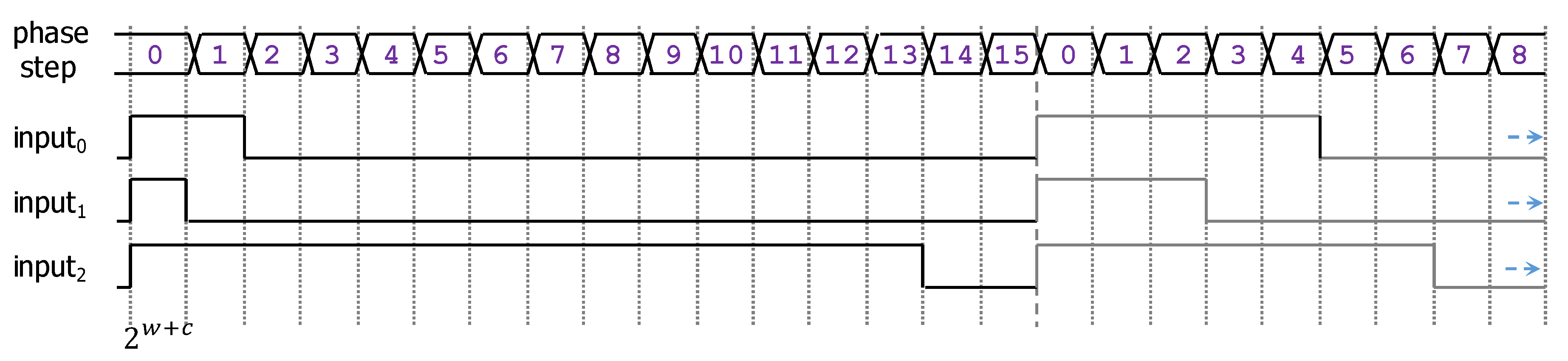
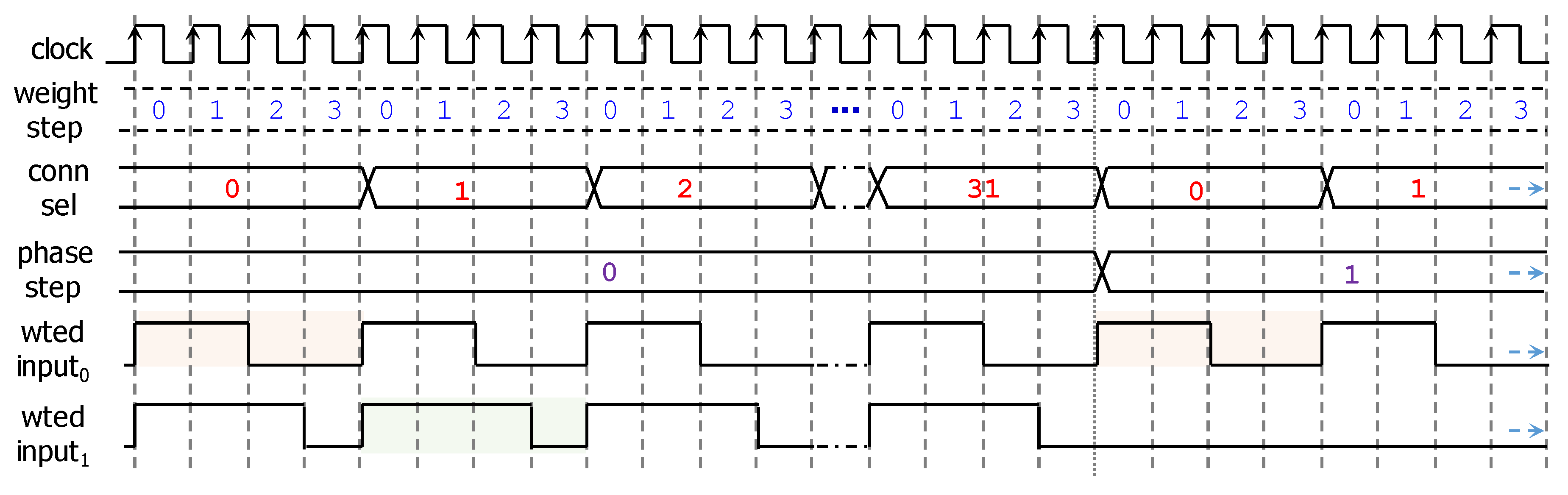
3.1.2. Duty-Cycle Encoding for the Neuron Inputs
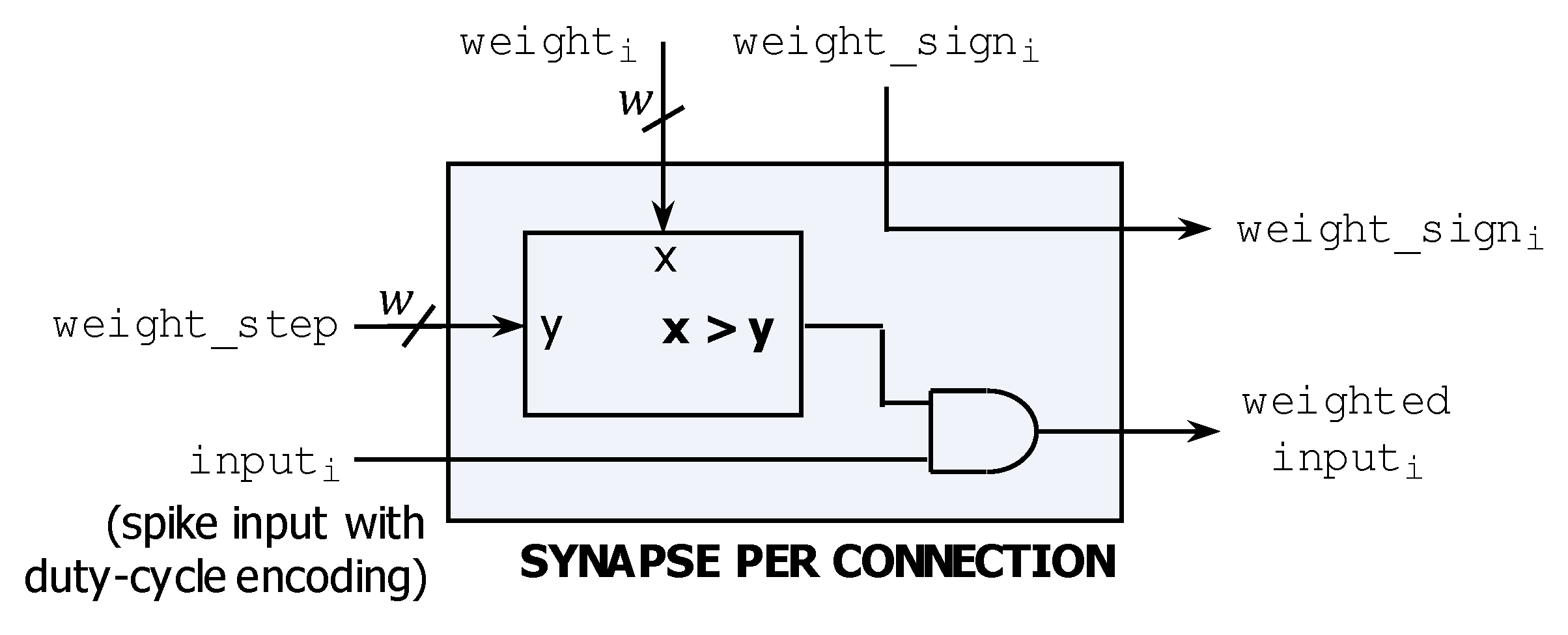
3.1.3. Weights (Connection Gain)
3.1.4. Bias
3.1.5. Computation of the Membrane Potential ()
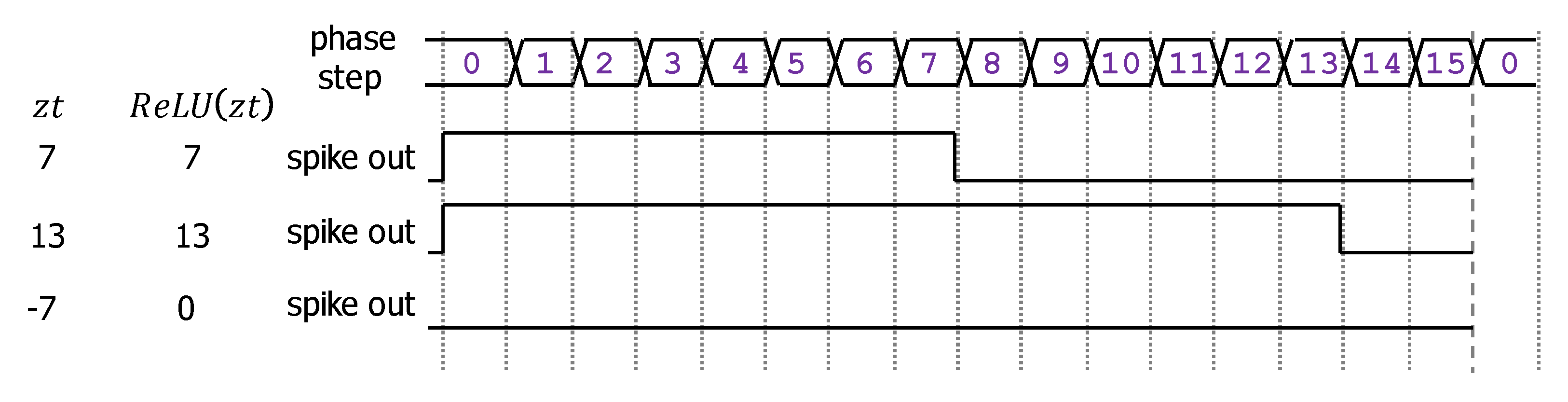
3.1.6. Output Activation Function
3.2. Implementation Details
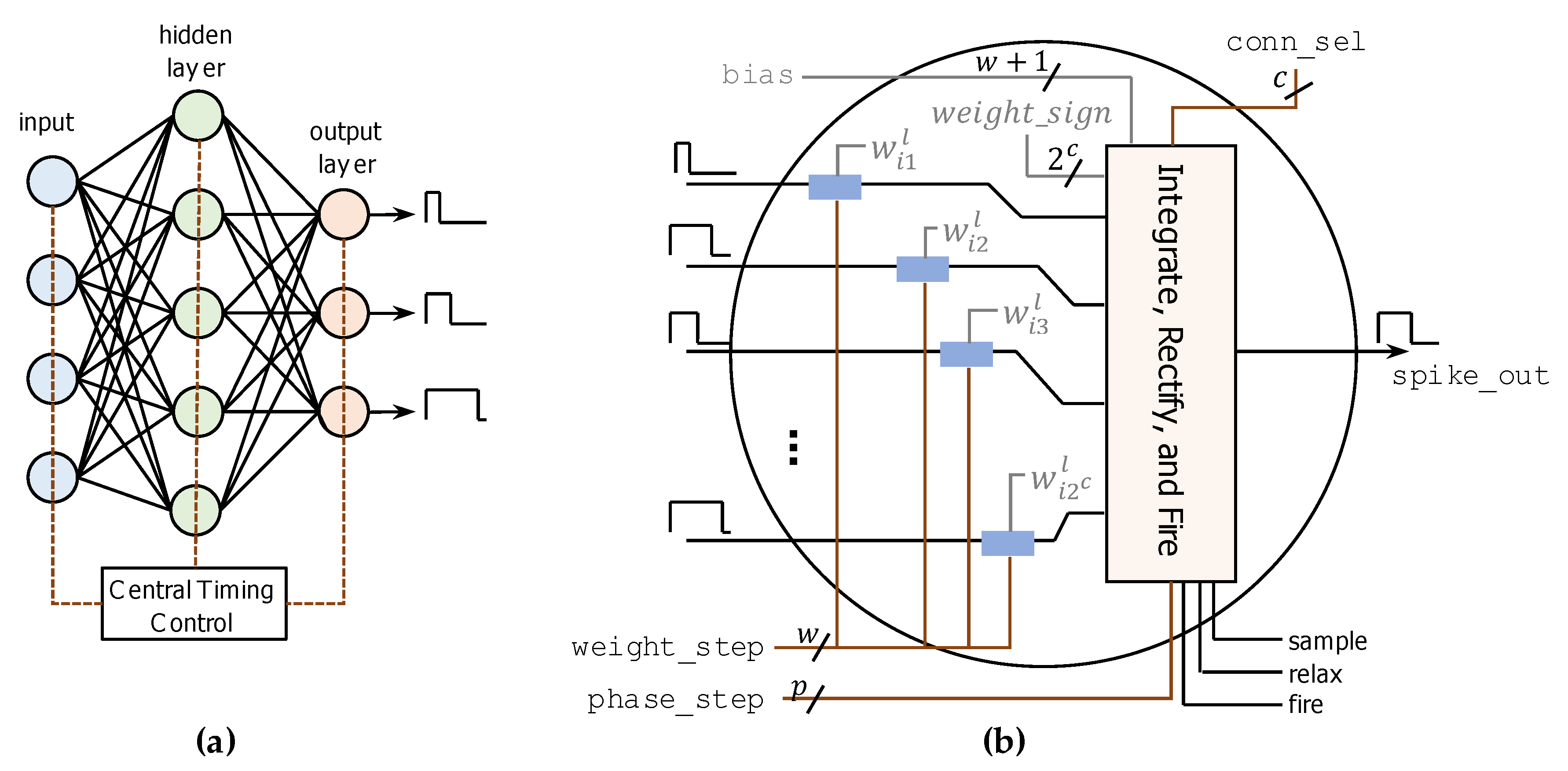
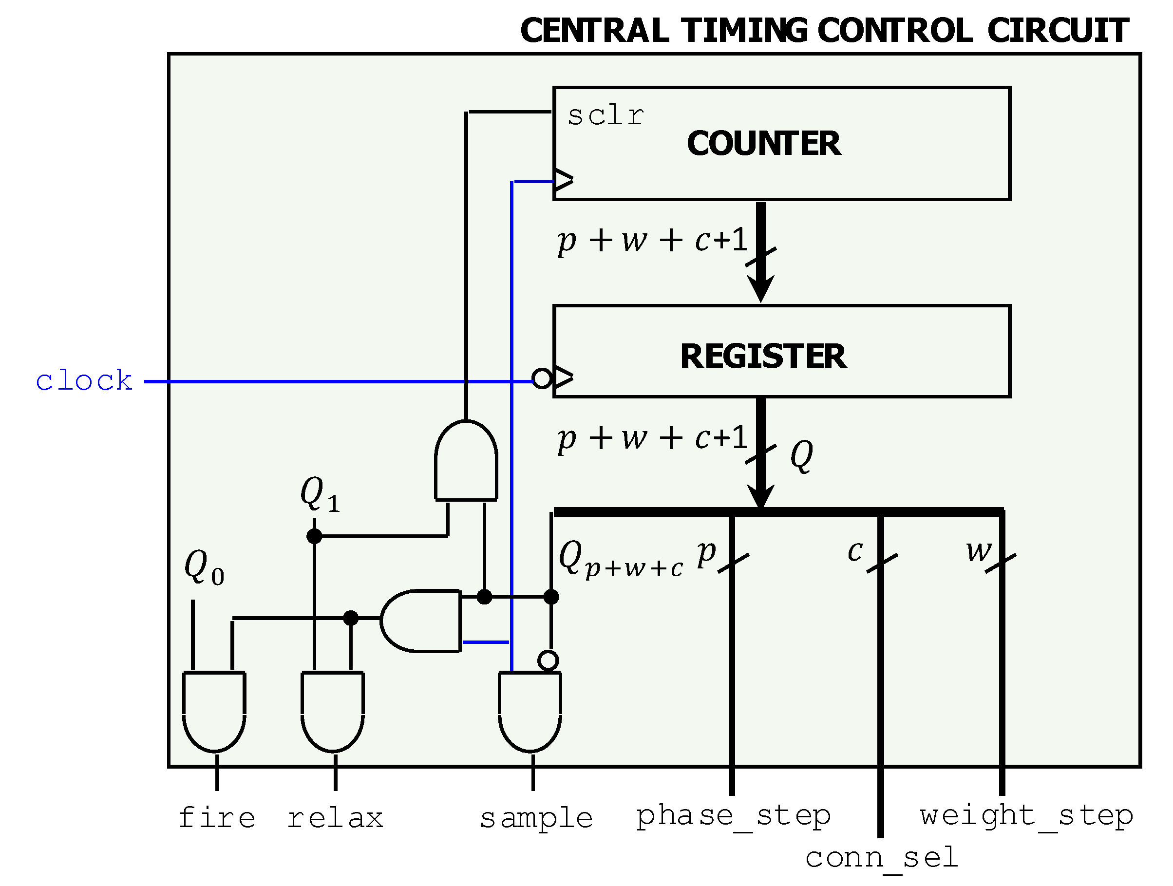
3.2.1. Central Timing Control Circuit
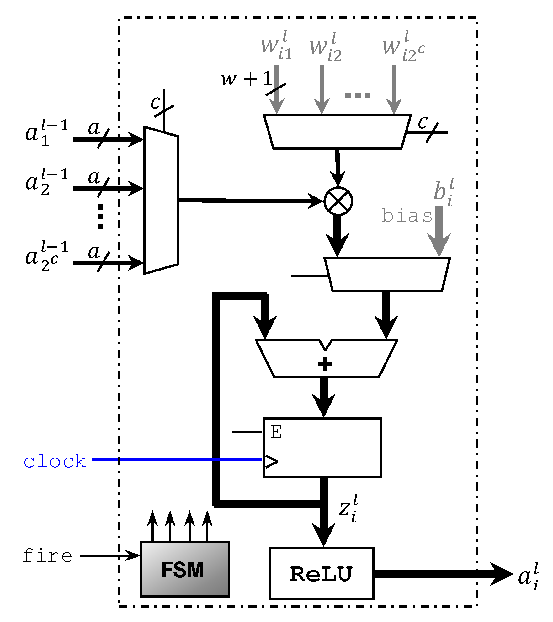
3.2.2. SHiNe Neuron—Multiplicative Effect of Each Connection Weight
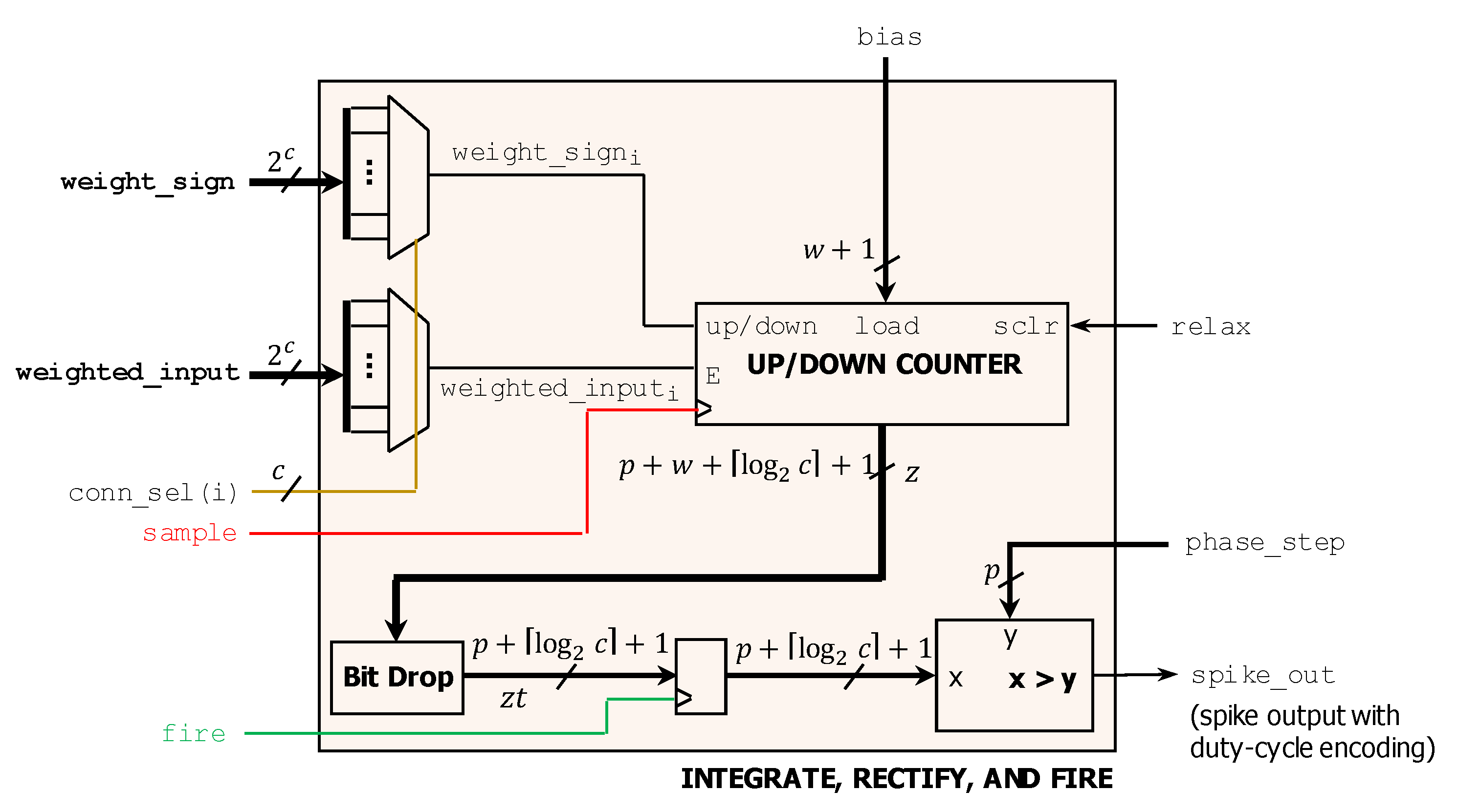
3.2.3. SHiNe Neuron—‘Integrate, Rectification and Fire’ Circuit
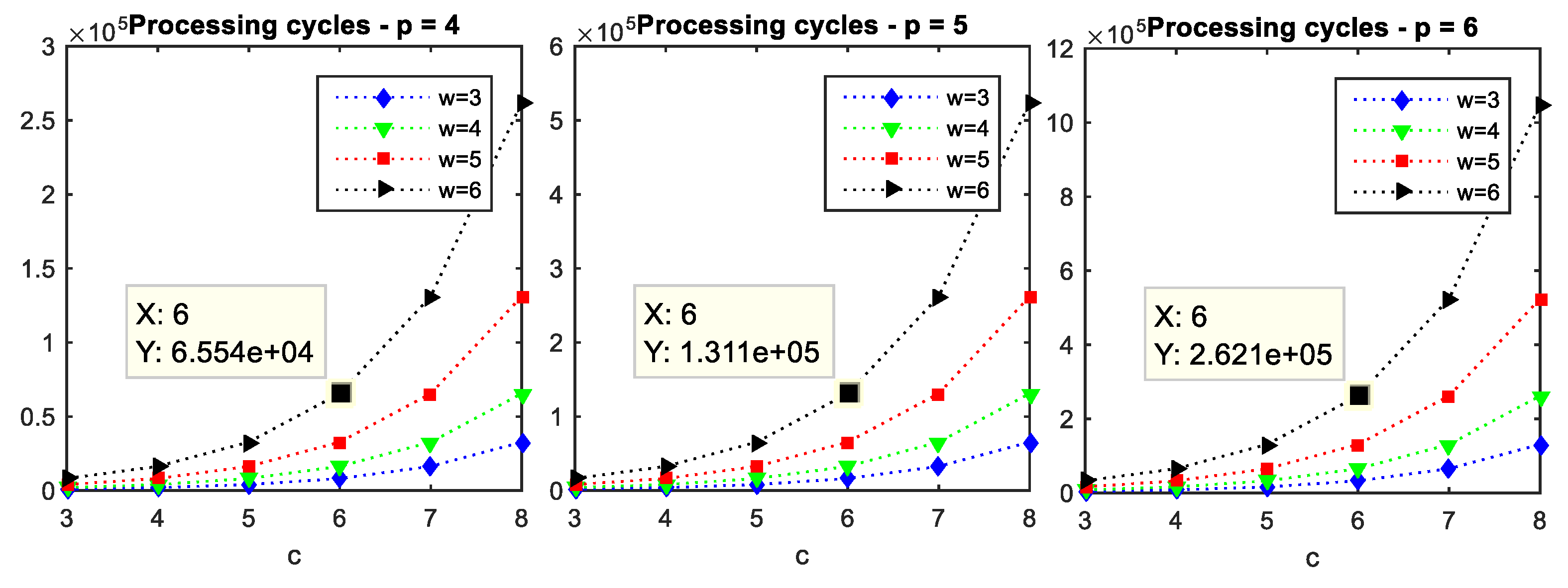
3.3. Hardware Processing Time
3.4. Training Approach and Software Tools
3.5. Circuit Synthesis and Simulation
3.5.1. Synthesis Details
- SHiNe_neuron.vhd: This code describes one neuron, assuming certain timing and control inputs, a set of input lines, input weights (sign and magnitude), and a signed bias value. All of these inputs are passed in from a higher-level module once it is instantiated. Bit-widths for several parameters are defined in a generic fashion. Once the fire input arrives, the new version of the output signal is prepared, and a relax resets the neuron to its biased initial value;
- ShiNe_ctrl.vhd: This is the Central Timing and Control Circuit that generates a set of multi-bit index signals, and some additional trigger signals, including sample, fire and relax. It includes a reset input so the control indexes can be reset to allow a frame to be processed at power-up;
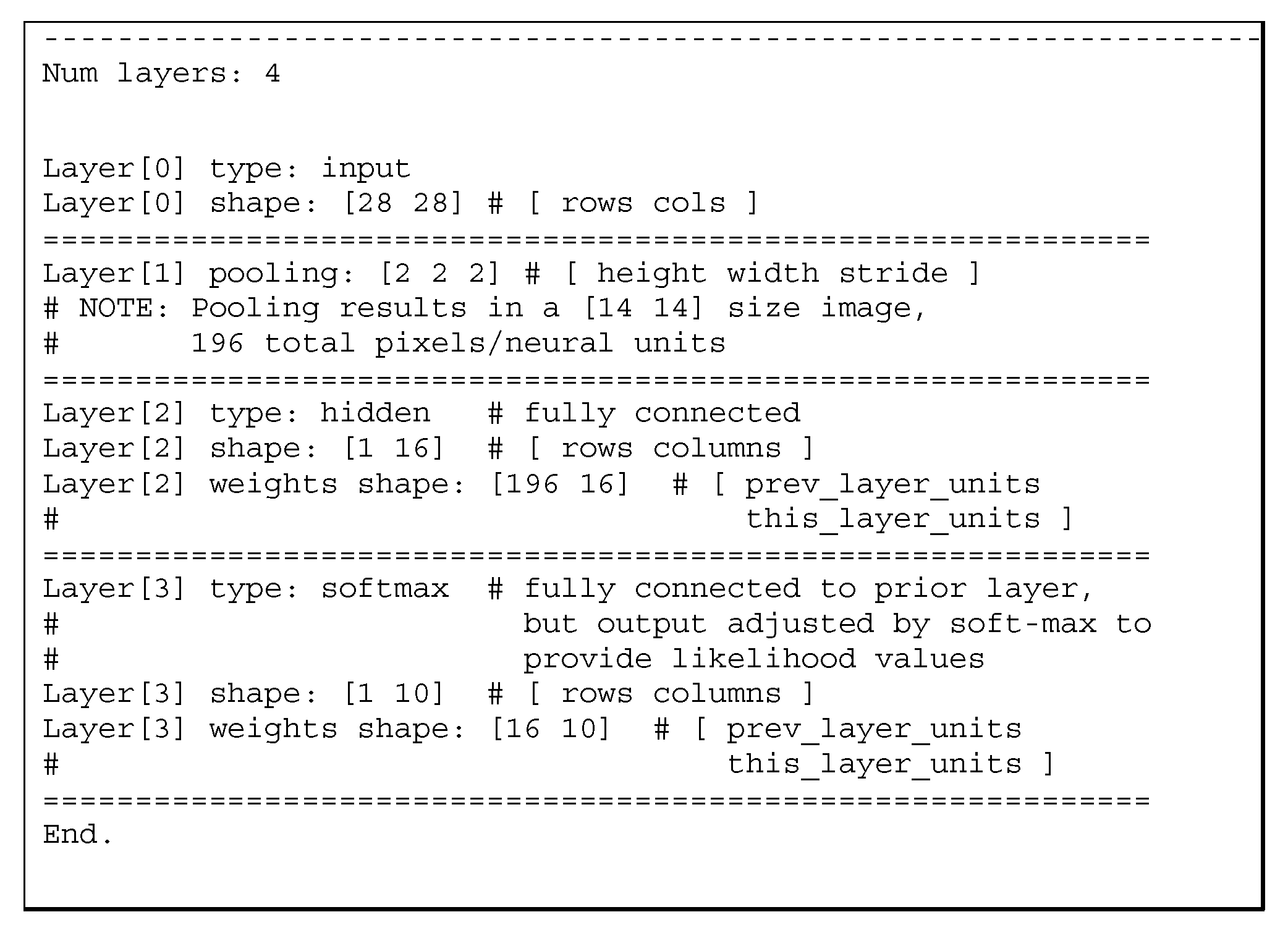
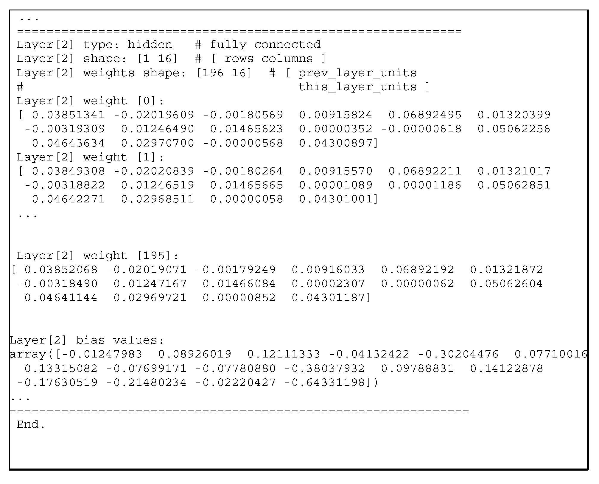
- top_{net name}_net.vhd: Automatically generated by cnn. This is the top-level circuit for a neural network. It instantiates the control circuit configured to specific bit-widths for the control indices, a set of neurons organized into layers according the network configuration file. The trained weight and bias are set as constant values that are fed into each neuron instance. If a connection is not needed because a prior layer has fewer units than the maximum allowed number of connections, the unused neurons inputs are tied to ‘0’;
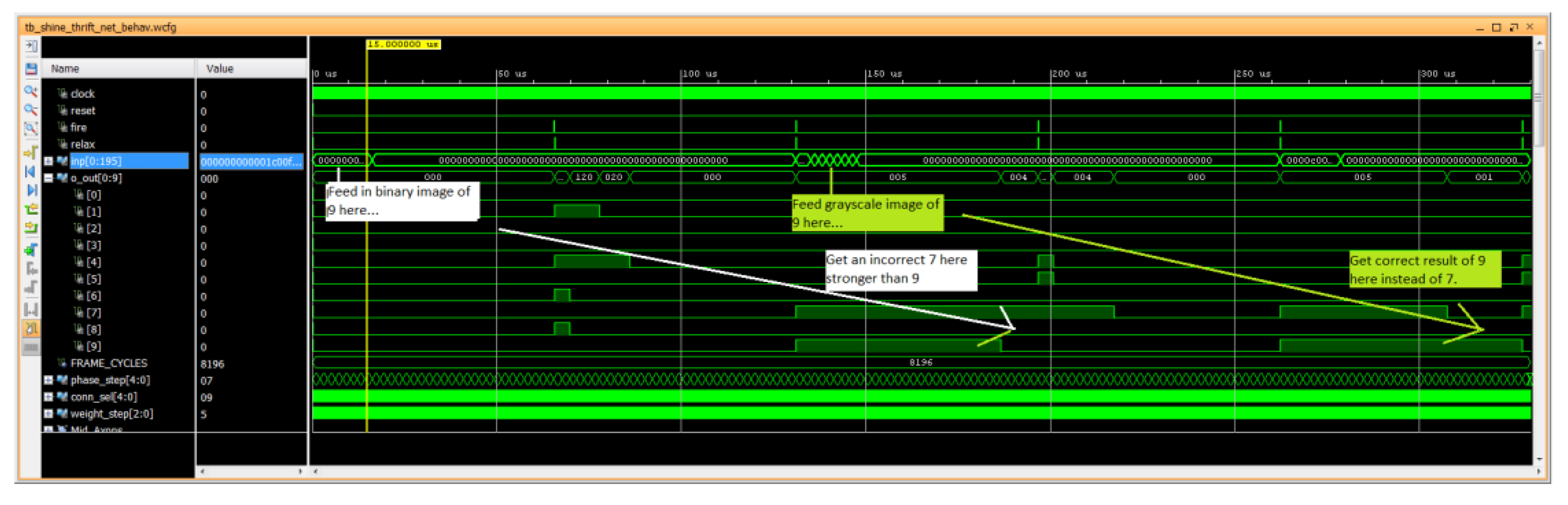
- tb_{net name}_net.vhd: This is the testbench for simulation. It feeds the input images (binary or grayscale) to the circuit so that the output lines can be retrieved at simulation. For example, in hand-digit recognition, we have an output line per each numeric digit we can recognize.
3.5.2. Simulation
4. Results
4.1. Neural Network Trade-Off Evaluation
4.1.1. Experiment with a Small Neural Network
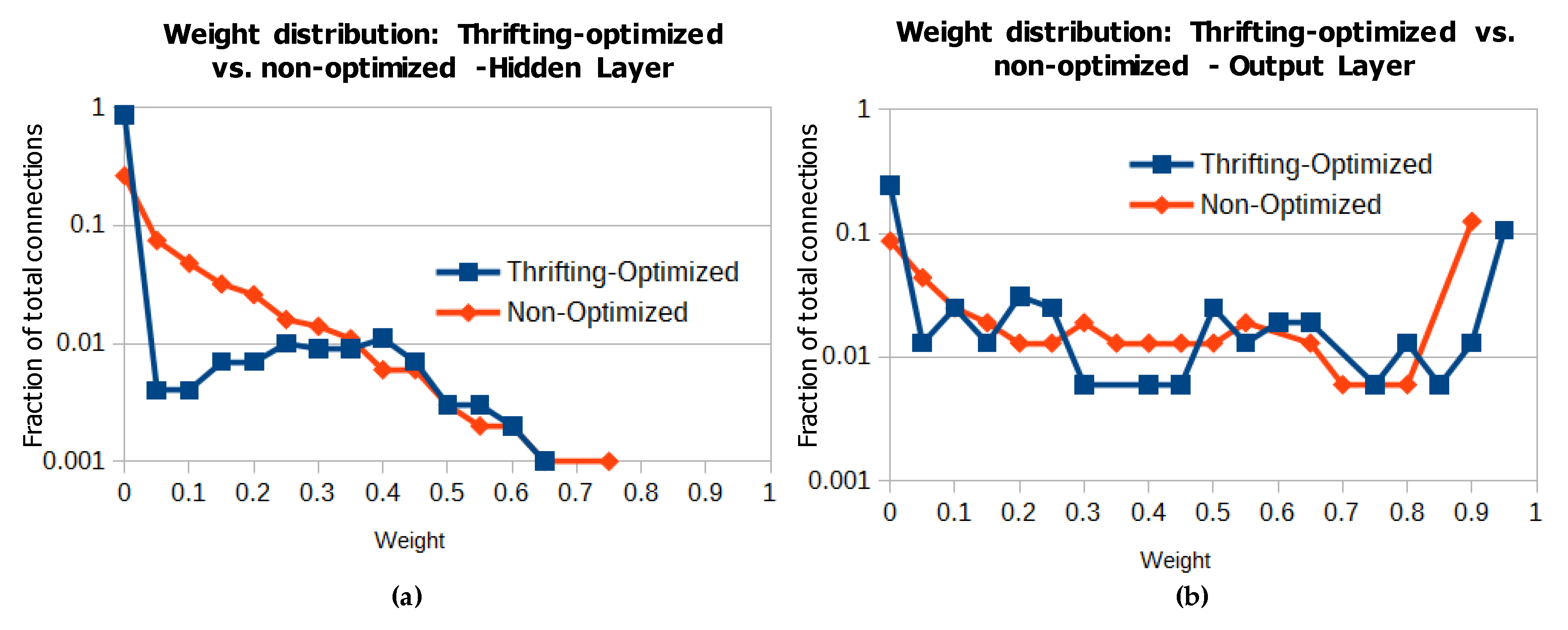
4.1.2. Thrifting to Reduce Hardware Resources
4.2. Hardware Accuracy (or Network Performance) Evaluation
4.3. Hardware Processing Time
4.4. Hardware Resources
4.5. Hardware Power Consumption
4.6. Power Consumption—Comparison with Other Implementations
5. Conclusions
Author Contributions
Funding
Conflicts of Interest
Appendix A
Appendix A.1. Available Neuron Types
- Input—always outs a specific value taken from a test data set, or real-world phenomenon.
- Convolution—a unit that applies convolution to a portion of a prior layer. A convolutional layer (not addressed in this work) may be arranged into multiple portions called feature maps.
- Pooling—a unit that passes a reduced version of the connected inputs, usually a compact set (e.g., 2 × 2). The most common pooling function is the max-pool, that achieves a down-sampling effect.
- Fully-Connected—a unit that can receive input from any unit in the prior layer, according to the weights. Weights are allowed to be zero, effectively meaning that it is disconnected.
- Soft-Max—a fully-connected unit with normalized output relative to all other units in the layer to emphasize a unit’s output in the layer and assign a likelihood-type value to each unit’s output.


- -p: Whether to print the network configuration before and after the training process (needed if one wants to capture training to a file).
- -d: Print additional intermediate values useful in debugging.
- -err: For each wrong classification result, print input image and classification info.
- -thrift{N}: Keep only the N largest-magnitude weights for each neuron (others are zeroed out) after loading a network configuration and before performance evaluation and optional training, and again after each optional training batch). N defaults to 32 if not specified.
- -pos: Whether to scale test inputs to non-negative values and assume non-negative only when printing graphical representations of layer activation levels.
- -q{n}: Whether to quantize weights, biases, and excitation/activation signal values so that it can be represented by fractional bits. Fractional step size is , and a real-value can be scaled up to an integer-equivalent by a factor of . Defaults to 4 if not specified.
- -m: Whether to limit weights to to and biases to to . Assumes quantization level set by -q or a default value of 1/16 quantization steps (4 fractional bits).
- -bininp{I}: Down-sample 2 × 2 patches of pixels and threshold the input pixel values at value of I to produce a binary image. ‘I’ should be an integer 0 to 255, or defaults to 200.
- -weightbins: Print a tabular histogram of the distribution of network weights, 0.05 per bin.
- -im{N}: Print a picture of the specified image number (0 to 59999 for the MNIST data), and a binary-thresholded version, according to the default threshold or the threshold set with the -bininp{I] option. N defaults to 0 if not provided.
- -one: Test only the image specified in the -imN option, print the expected (labeled) result and actual network-classified result, then quit.
- -train: Perform training. The best-performing overall weight and bias set from each training and evaluation batch is remembered then used during the network configuration printing if enabled by the -p option. Print summary metrics of the training and evaluation at each batch.
- -bN: Train up to N batches, each of which has 500 trials of an image selected randomly from the 50000 training examples in the MNIST data set, followed by back-propagation. The batch of training is followed by a full 10000 image performance assessment. N must be specified, but if -b is not used, the default batch limit is 5000.
- -etaF: Set the training rate eta to the floating-point value F (0.005 by default). Eta is how much of the full back-propagation error correction to apply to each weight after each training image is presented, and can be thought of as how ‘fast’ to descend the local error surface gradient.
- -etafactorF: How much of eta to keep after each training batch once the overall performance is at least 80% correct. F should be a factor between 0.0 and 1.0. The default Eta factor is 0.999.
- -weightdecayF: At each training step where the root mean square (RMS) of weights are >0.25, weights will be decayed by this much (multiplicative factor of 1.0 −F). F can be thought of fractional loss at each training step, and it is 0.004 (0.4%) by default, and is intended to keep weights relatively small and bounded through the training period.
- -vhdl: Generate a VHDL top-level circuit with the proper layers of SHiNe neurons, connected as per the thrifting limit, with connections weights and biased according to the trained parameters. The current implementation is limited to two active layers after both an input and down-sampling (max-pool) layer.
- -fxp_vhdl: Generate a VHDL top-level circuit with the correct layers of fixed-point multiply-and accumulate neurons, connected according to the thrifting limit (e.g., fan-in of 32), with connections weighted and biased according to the trained parameters.
- -xray{I},{J}: Print details about how each connection is contributing to unit J’s activation in layer I. Note: only fully-connected or soft-max layers are supported.
Appendix A.2. Compile-Time Options
References
- Chen, Y.; Krishna, T.; Emer, J.S.; Sze, V. Eyeriss: An Energy-Efficient Reconfigurable Accelerator for Deep Convolutional Neural Networks. IEEE J. Solid State Circuits 2017, 52, 127–138. [Google Scholar] [CrossRef]
- Zhang, C.; Li, P.; Sun, G.; Guan, Y.; Xiao, B.; Cong, J. Optimizing FPGA-based Accelerator Design for Deep Convolutional Neural Networks. In Proceedings of the 2015 ACM/SIGDA International Symposium on Field-Programmable Gate Arrays, Monterey, CA, USA, 22–24 February 2015; ACM: New York, NY, USA, 2015; pp. 161–170. [Google Scholar]
- Chakradhar, S.; Sankaradas, M.; Jakkula, V.; Cadambi, S. A dynamically configurable coprocessor for convolutional neural networks. ACM SIGARCH Comput. Archit. News 2010, 38, 247–257. [Google Scholar] [CrossRef]
- Hardieck, M.; Kumm, M.; Möller, K.; Zipf, P. Reconfigurable Convolutional Kernels for Neural Networks on FPGAs. In Proceedings of the 2019 ACM/SIGDA International Symposium on Field-Programmable Gate Arrays, Seaside, CA, USA, 24–26 February 2019; ACM: New York, NY, USA, 2019; pp. 43–52. [Google Scholar]
- Markidis, S.; Chien, S.; Laure, E.; Pong, I.; Vetter, J.S. NVIDIA Tensor Core Programmability, Performance & Precision. In Proceedings of the 2018 IEEE International Parallel and Distributed Processing Symposium Workshops, Vancouver, BC, Canada, 21–25 May 2018. [Google Scholar]
- Misra, J.; Saha, I. Artificial neural networks in hardware: A survey of two decades of progress. Neurocomputing 2010, 74, 239–255. [Google Scholar] [CrossRef]
- Renteria-Cedano, J.; Rivera, J.; Sandoval-Ibarra, F.; Ortega-Cisneros, S.; Loo-Yau, R. SoC Design Based on a FPGA for a Configurable Neural Network Trained by Means of an EKF. Electronics 2019, 8, 761. [Google Scholar] [CrossRef]
- Nurvitadhi, E.; Venkatesh, G.; Sim, J.; Marr, D.; Huang, R.; Hock, J.O.G.; Liew, Y.T.; Srivatsan, K.; Moss, D.; Subhaschandra, S.; et al. Can FPGAs beat GPUs in accelerating next-generation Deep Neural Networks? In Proceedings of the 2017 ACM/SIGDA International Symposium on Field-Programmable Gate Arrays, Monterey, CA, USA, 22–24 February 2017; ACM: New York, NY, USA, 2017; pp. 5–14. [Google Scholar]
- Gomperts, A.; Ukil, A.; Zurfluh, F. Development and Implementation of Parameterized FPGA-Based General-Purpose Neural Networks for Online Applications. IEEE Trans. Ind. Inform. 2011, 7, 78–89. [Google Scholar] [CrossRef]
- Himavathi, S.; Anitha, D.; Muthuramalingam, A. Feedforward Neural Network Implementation in FPGA using layer multiplexing for effective resource utilization. IEEE Trans. Neural Netw. 2007, 18, 880–888. [Google Scholar] [CrossRef] [PubMed]
- Tavanaei, A.; Ghodrati, M.; Kheradpisheh, S.R.; Masquelier, T.; Maida, A.S. Deep Learning in Spiking Neural Networks. Neural Netw. 2019, 111, 47–63. [Google Scholar] [CrossRef] [PubMed]
- Iakymchuk, T.; Rosado, A.; Frances, J.V.; Batallre, M. Fast Spiking Neural Network Architecture for low-cost FPGA devices. In Proceedings of the 7th International Workshop on Reconfigurable and Communication-Centric Systems-on-Chip (ReCoSoC), York, UK, 9–11 July 2012. [Google Scholar]
- Rice, K.; Bhuiyan, M.A.; Taha, T.M.; Vutsinas, C.N.; Smith, M. FPGA Implementation of Izhikevich Spiking Neural Networks for Character Recognition. In Proceedings of the 2019 International Conference on Reconfigurable Computing and FPGAs, Cancun, Mexico, 9–11 December 2009. [Google Scholar]
- Pearson, M.J.; Pipe, A.G.; Mitchinson, B.; Gurney, K.; Melhuish, C.; Gilhespy, I.; Nibouche, N. Implementing Spiking Neural Networks for Real-Time Signal Processing and Control Applications. IEEE Trans. Neural Netw. 2007, 18, 1472–1487. [Google Scholar] [CrossRef] [PubMed]
- Belyaev, M.; Velichko, A. A Spiking Neural Network Based on the Model of VO2-Neuron. Electronics 2019, 8, 1065. [Google Scholar] [CrossRef]
- Arbib, M.A. The Handbook of Brain Theory and Neural Networks, 2nd ed.; MIT Press: Cambridge, MA, USA, 2002. [Google Scholar]
- Nielsen, M.A. Neural Networks and Deep Learning; Determination Press: San Francisco, CA, USA, 2015. [Google Scholar]
- Minsky, M.L.; Papert, S.A. Perceptrons: An Introduction to Computational Geometry, 3rd ed.; MIT Press: Cambridge, MA, USA, 2017. [Google Scholar]
- Glorot, X.; Bordes, A.; Bengio, Y. Deep sparse rectifier neural networks. In Proceedings of the 14th International Conference on Artificial Intelligence and Statistics, Ft. Lauderdale, FL, USA, 11–13 April 2011; pp. 315–323. [Google Scholar]
- Deng, L. The MNIST database of handwritten digit images for machine learning research [best of web]. IEEE Signal Process. Mag. 2012, 29, 141–142. [Google Scholar] [CrossRef]
- Lecun, Y.; Bottou, L.; Bengio, Y.; Haffner, P. Gradient-based learning applied to document recognition. Proc. IEEE 1998, 86, 2278–2324. [Google Scholar] [CrossRef]
- Llamocca, D. Self-Reconfigurable Architectures for HEVC Forward and Inverse Transform. J. Parallel Distrib. Comput. 2017, 109, 178–192. [Google Scholar] [CrossRef]
- Reagen, B.; Whatmough, P.; Adolf, R.; Rama, S.; Lee, H.; Lee, S.; Hernandez-Lobato, J.; Wei, G.; Brooks, D. Minerva: Enabling Low-Power, Highly-Accurate Deep Neural Network Accelerators. In Proceedings of the 2016 ACM/IEEE 43rd Annual International Symposium on Computer Architecture (ISCA), Seoul, Korea, 18–22 June 2016. [Google Scholar]
- Gokhale, V.; Jin, J.; Dundar, A.; Martini, B.; Culurciello, E. A 240 G-Ops/s mobile coprocessor for deep neural networks. In Proceedings of the 2014 IEEE Conference on Computer Vision and Pattern Recognition Workshops, Columbus, OH, USA, 23–28 June 2014. [Google Scholar]
- Farabet, C.; Martini, B.; Akselrod, P.; Talay, S.; LeCun, Y.; Culurciello, E. Hardware accelerated convolutional neural networks for synthetic vision systems. In Proceedings of the 2010 IEEE International Symposium on Circuits and Systems, Paris, France, 30 May–2 June 2010. [Google Scholar]
- Umuroglu, Y.; Fraser, N.J.; Gambardella, G.; Blott, M.; Leong, P.; Jahre, M.; Vissers, K. FINN: A framework for Fast, Scalable Binarized Neural Network Interface. In Proceedings of the 2017 ACM/SIGDA International Symposium on Field-Programmable Gate Arrays, Monterey, CA, USA, 22–24 February 2017; ACM: New York, NY, USA, 2017; pp. 65–74. [Google Scholar]
- Strigl, D.; Kofler, K.; Podlipnig, S. Performance and scalability of GPU-based convolutional neural networks. In Proceedings of the 2018 18th Euromicro Conference on Parallel, Distributed and Network-based Processing, Pisa, Italy, 17–19 February 2010. [Google Scholar]
- Song, S.; Su, C.; Rountree, B.; Cameron, K.W. A simplified and accurate model of power-performance efficiency on emergent GPU architectures. In Proceedings of the 2013 IEEE 27th International Symposium on Parallel and Distributed Processing, Boston, MA, USA, 20–24 May 2013. [Google Scholar]
- Hauswald, J.; Kang, Y.; Laurenzano, M.A.; Chen, Q.; Li, C.; Mudge, T.; Dreslinski, R.; Mars, J.; Tang, L. DjiNN and Tonic: DNN as a service and its implications for future warehouse scale computers. In Proceedings of the 2015 ACM/IEEE 42nd Annual International Symposium on Computer Architecture (ISCA), Portland, OR, USA, 13–17 June 2015. [Google Scholar]


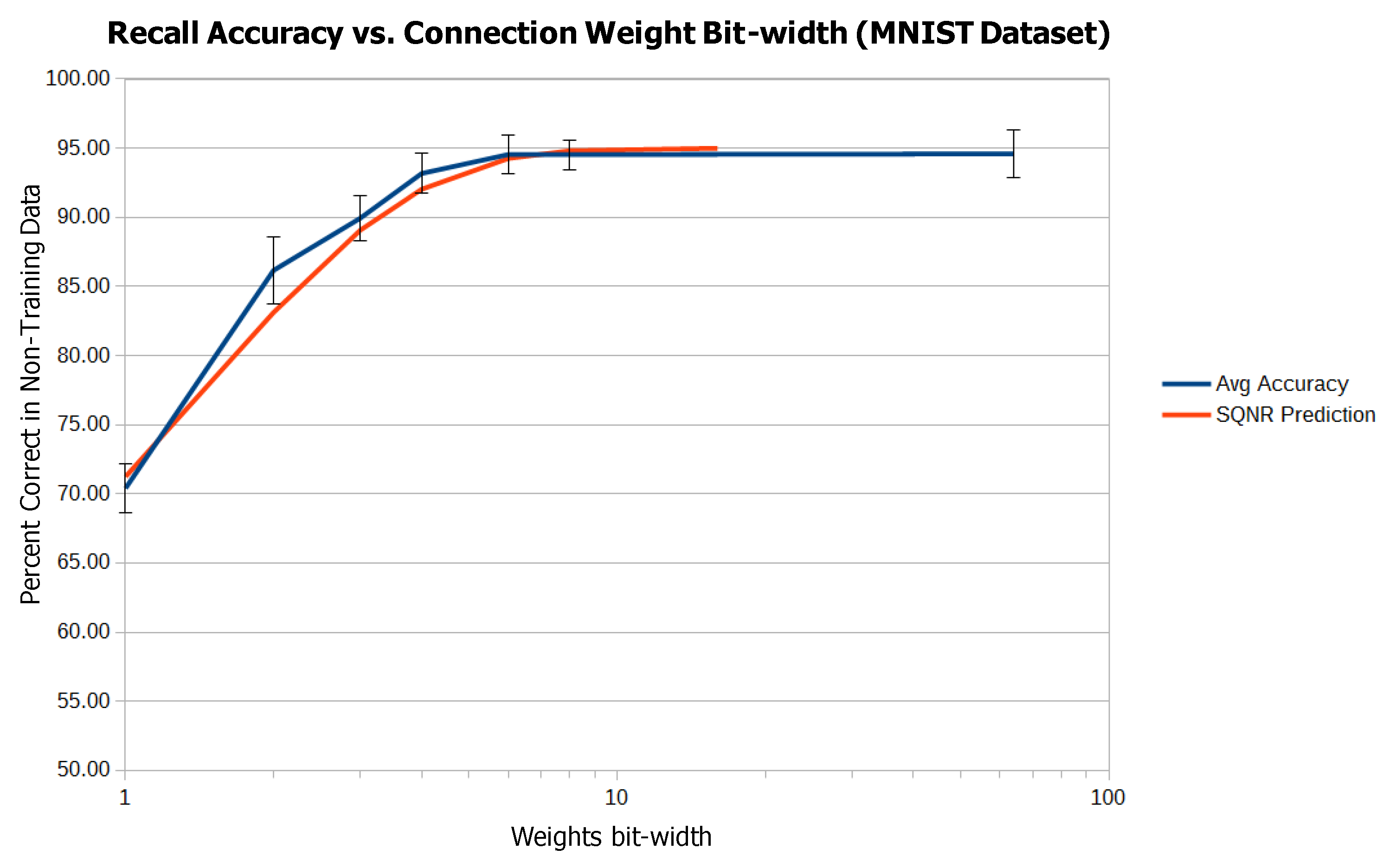
| Bits Per Connection | Average Accuracy (%) |
|---|---|
| 0 | 26.67 |
| 1 | 70.42 |
| 2 | 86.17 |
| 3 | 89.94 |
| 4 | 93.17 |
| 6 | 94.57 |
| 8 | 94.54 |
| 64 | 94.60 |
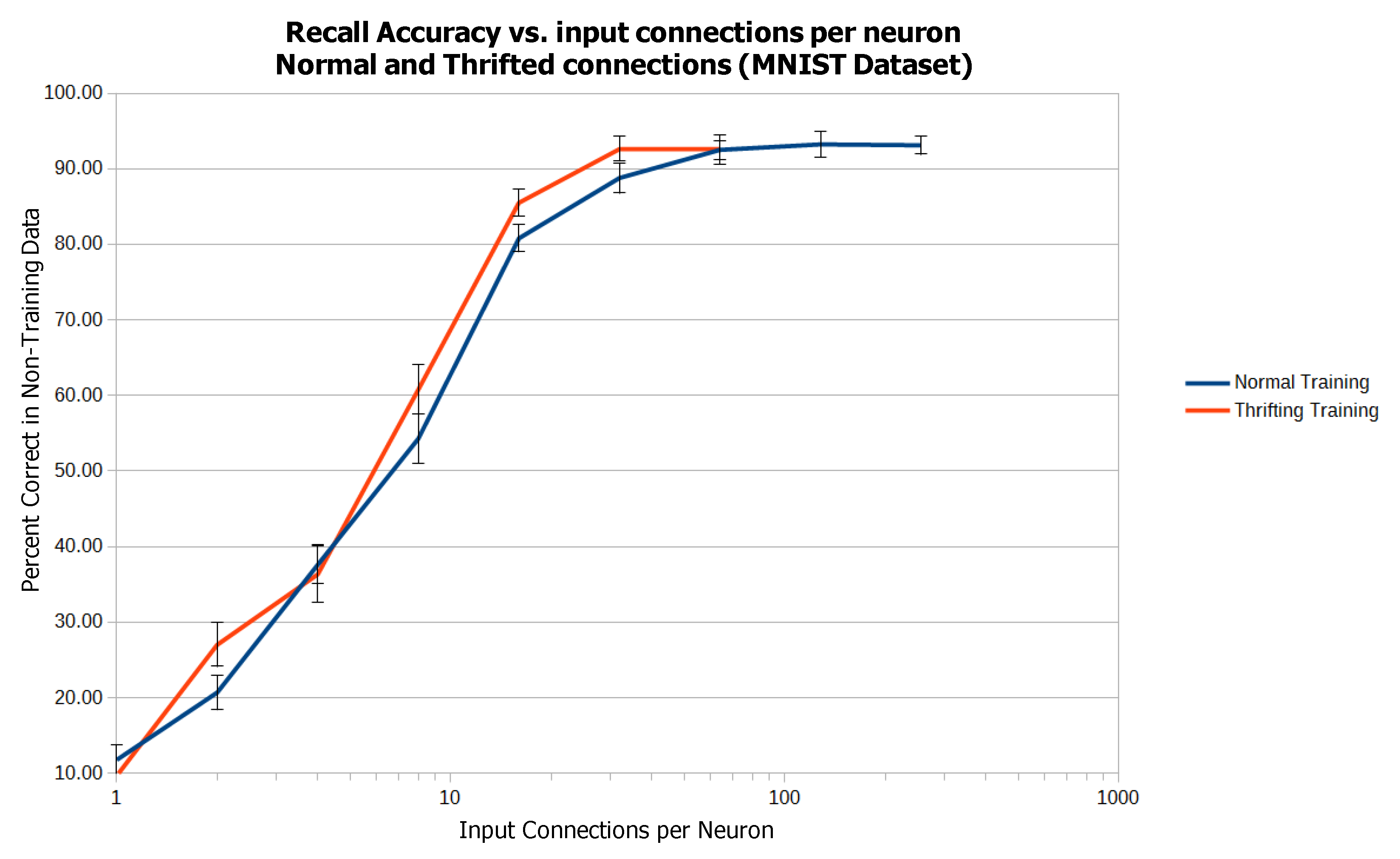
| Fan-In | Normal Training (%) | Thrifted Training (%) |
|---|---|---|
| 1 | 11.78 | 9.67 |
| 2 | 20.69 | 27.01 |
| 4 | 37.61 | 36.33 |
| 8 | 54.28 | 60.79 |
| 16 | 80.79 | 85.50 |
| 32 | 88.78 | 92.65 |
| 64 | 92.51 | 92.54 |
| 128 | 93.24 | |
| 256 | 93.12 |
| Network | Name | Input Layer | Hidden Layer | Output Layer |
|---|---|---|---|---|
| 1 | SHiNe_f16_m10_net | 196 | 16 | 10 |
| 2 | SHiNe_f32_m10_net | 196 | 32 | 10 |
| 3 | SHiNe_f64_m10_net | 196 | 64 | 10 |
| Pass | Tie | Fail | Total | |
|---|---|---|---|---|
| Tallies | 39 | 1 | 3 | 43 |
| SHiNe (vhdl) % | 90.70% | 2.33% | 6.98% | |
| C-Sim % | 91.97% | For grayscale input images | ||
| C-Sim % | 89.60% | For Binary-thresholded input images | ||
| Neurons | FXP_N | SHinE | SHiNe Hardware (LUT) Savings (%) | |||
|---|---|---|---|---|---|---|
| LUTs | FFs | LUTs | FFs | |||
| 1 | 16 + 10 = 26 | 1635 | 720 | 814 | 646 | 50.1% |
| 2 | 32 + 10 = 42 | 1955 | 930 | 1091 | 824 | 44.1% |
| 3 | 64 + 10 = 74 | 2402 | 1260 | 1335 | 1003 | 44.2% |
| Neural Network | Neurons | FXP_N | SHinE | % of Design Power Savings of SHiNe | ||
|---|---|---|---|---|---|---|
| Design Power | Total Power | Design Power | Total Power | |||
| 1 | 16 + 10 = 26 | 90 | 182 | 69 | 161 | 23.3% |
| 2 | 32 + 10 = 42 | 79 | 171 | 60 | 152 | 24.1% |
| 3 | 64 + 10 = 74 | 66 | 158 | 50 | 142 | 24.2% |
| Work | Platform | Power | Details | |
|---|---|---|---|---|
| [23] | ASIC | 18.3 mW | 40 nm CMOS technology | CNN, fixed point |
| Ours | FPGA | 161 mW | Estimated power of the design | ANN (SHiNe_f64), 196 × 196 image |
| [24] | FPGA | 4000 mW | Device power: Zynq XC7Z045 Zynq (ARM-Cortex + FPGA) + memory | CNN, fixed point, 500 × 350 image |
| [25] | FPGA | 15 W | Power of a custom board: Virtex-4 SX35 FPGA + QDR-SRAM. | CNN 500 × 500 image |
| [26] | FPGA | 7.3W | Power of the XC7Z045 device | Binarized Neural Network (BNN) |
| [25] | CPU | 90 W | Core 2 Duo CPU | CNN |
| [27] | CPU | 95 W | Core i7 860 CPU | CNN |
| [28] | GPU | 133 W | Tesla C2075 GPU | ANN |
| [29] | GPU | 240 W | K40 GPU | CNN |
| [27] | GPU | 216 W | GeForce GTX 275 GPU | CNN |
© 2019 by the authors. Licensee MDPI, Basel, Switzerland. This article is an open access article distributed under the terms and conditions of the Creative Commons Attribution (CC BY) license (http://creativecommons.org/licenses/by/4.0/).
Share and Cite
Losh, M.; Llamocca, D. A Low-Power Spike-Like Neural Network Design. Electronics 2019, 8, 1479. https://doi.org/10.3390/electronics8121479
Losh M, Llamocca D. A Low-Power Spike-Like Neural Network Design. Electronics. 2019; 8(12):1479. https://doi.org/10.3390/electronics8121479
Chicago/Turabian StyleLosh, Michael, and Daniel Llamocca. 2019. "A Low-Power Spike-Like Neural Network Design" Electronics 8, no. 12: 1479. https://doi.org/10.3390/electronics8121479
APA StyleLosh, M., & Llamocca, D. (2019). A Low-Power Spike-Like Neural Network Design. Electronics, 8(12), 1479. https://doi.org/10.3390/electronics8121479