A Low-Voltage Multi-Band ZigBee Transceiver


Abstract
1. Introduction
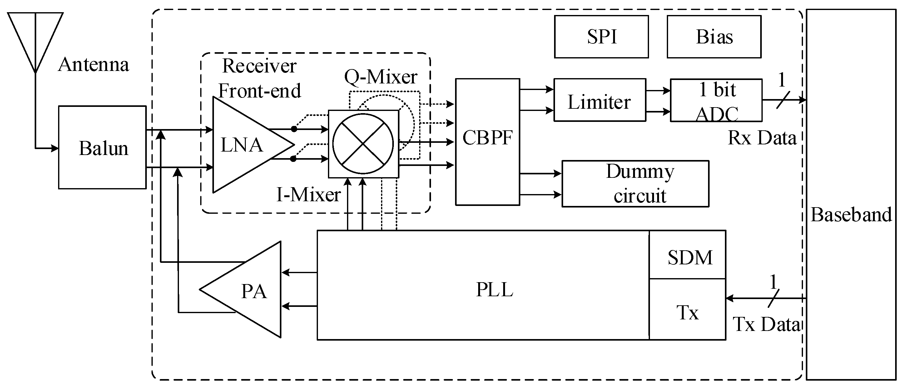
2. ZigBee Transceiver Architecture
2.1. Transceiver Architecture
2.2. System Consideration
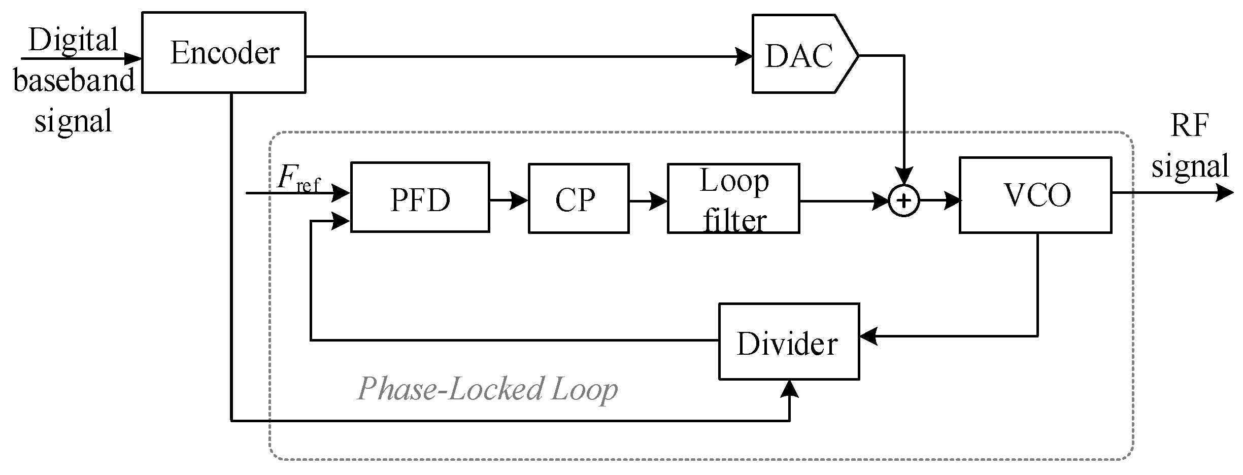
3. Transmitter Design
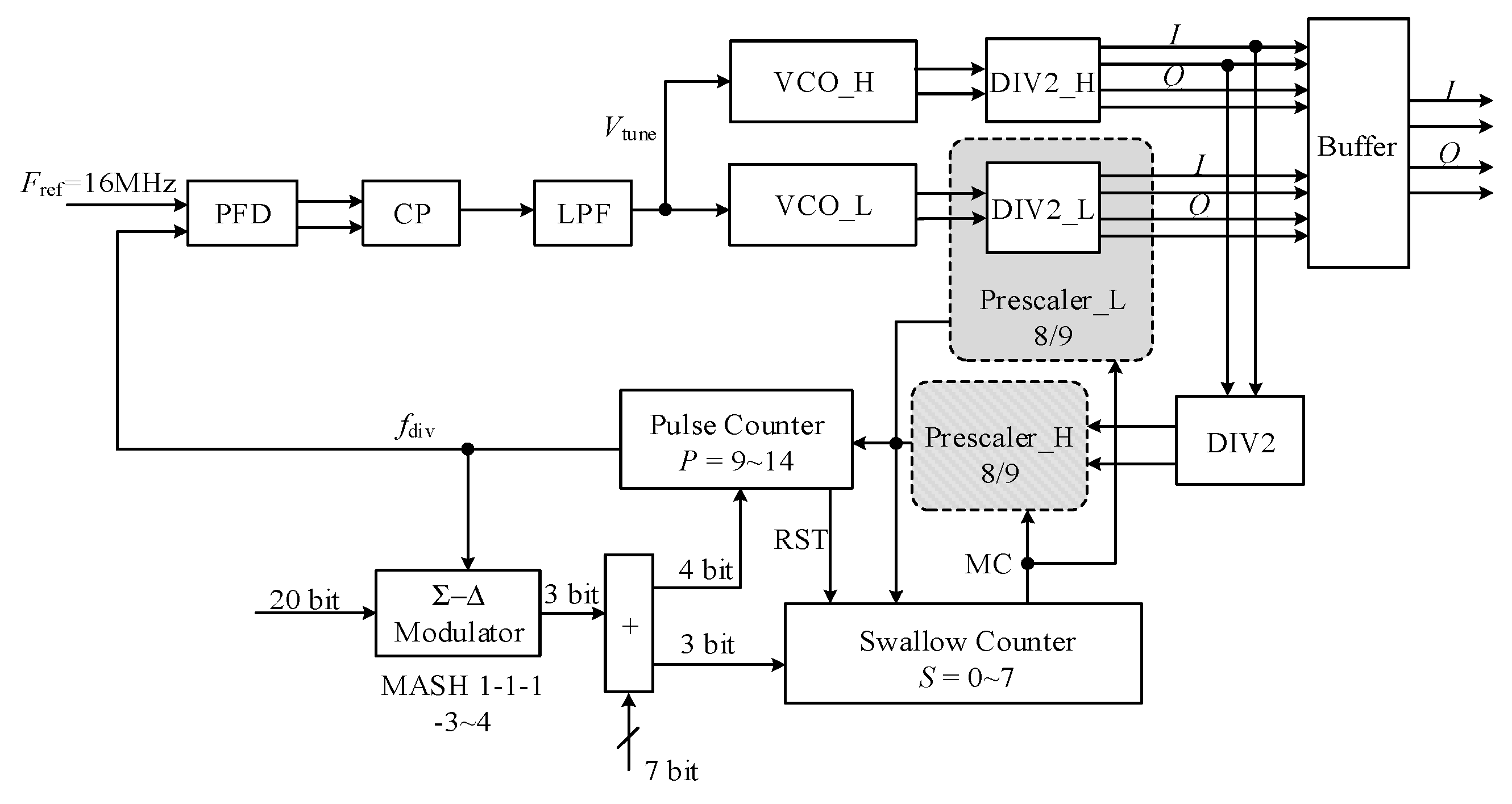
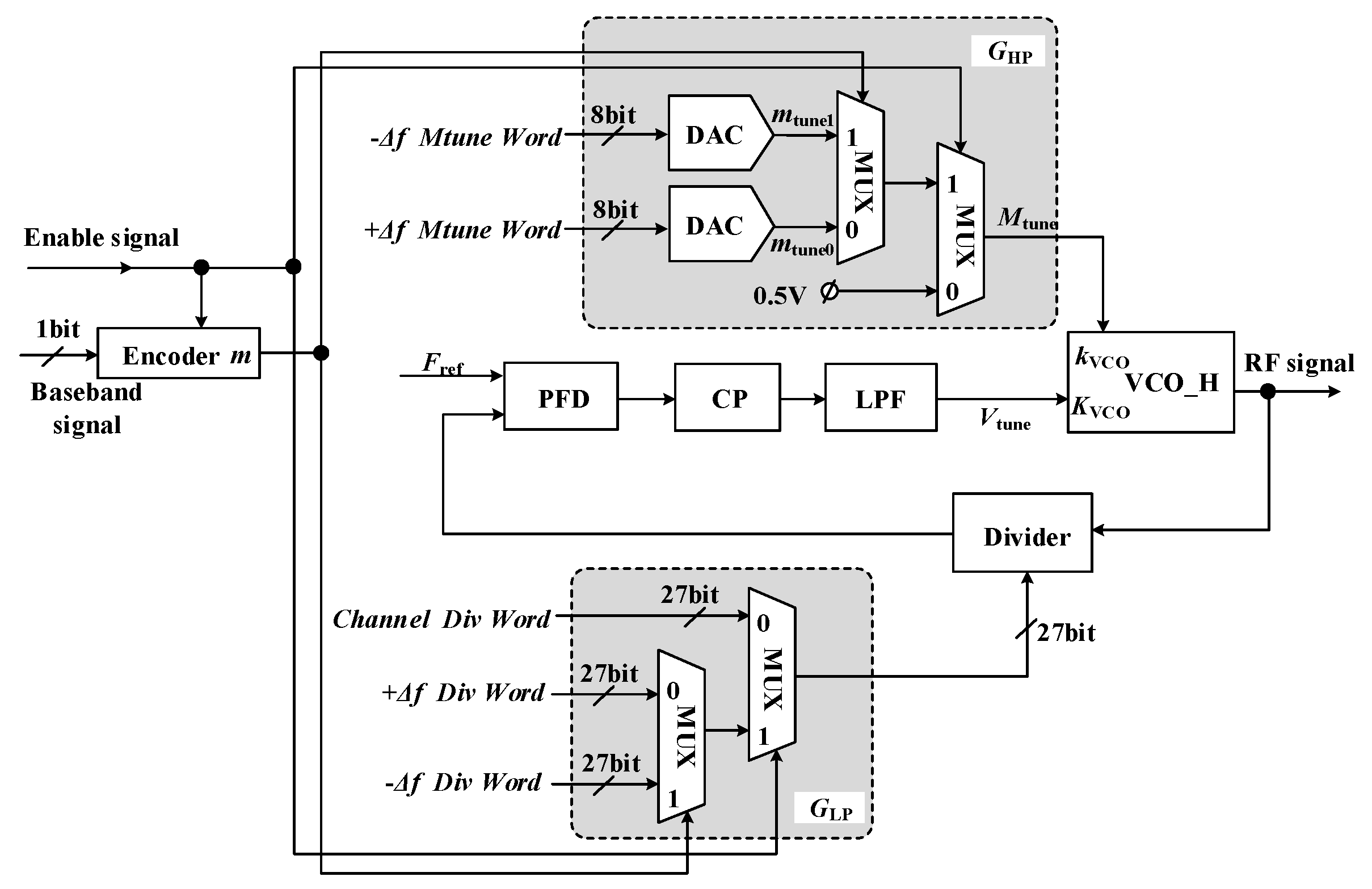
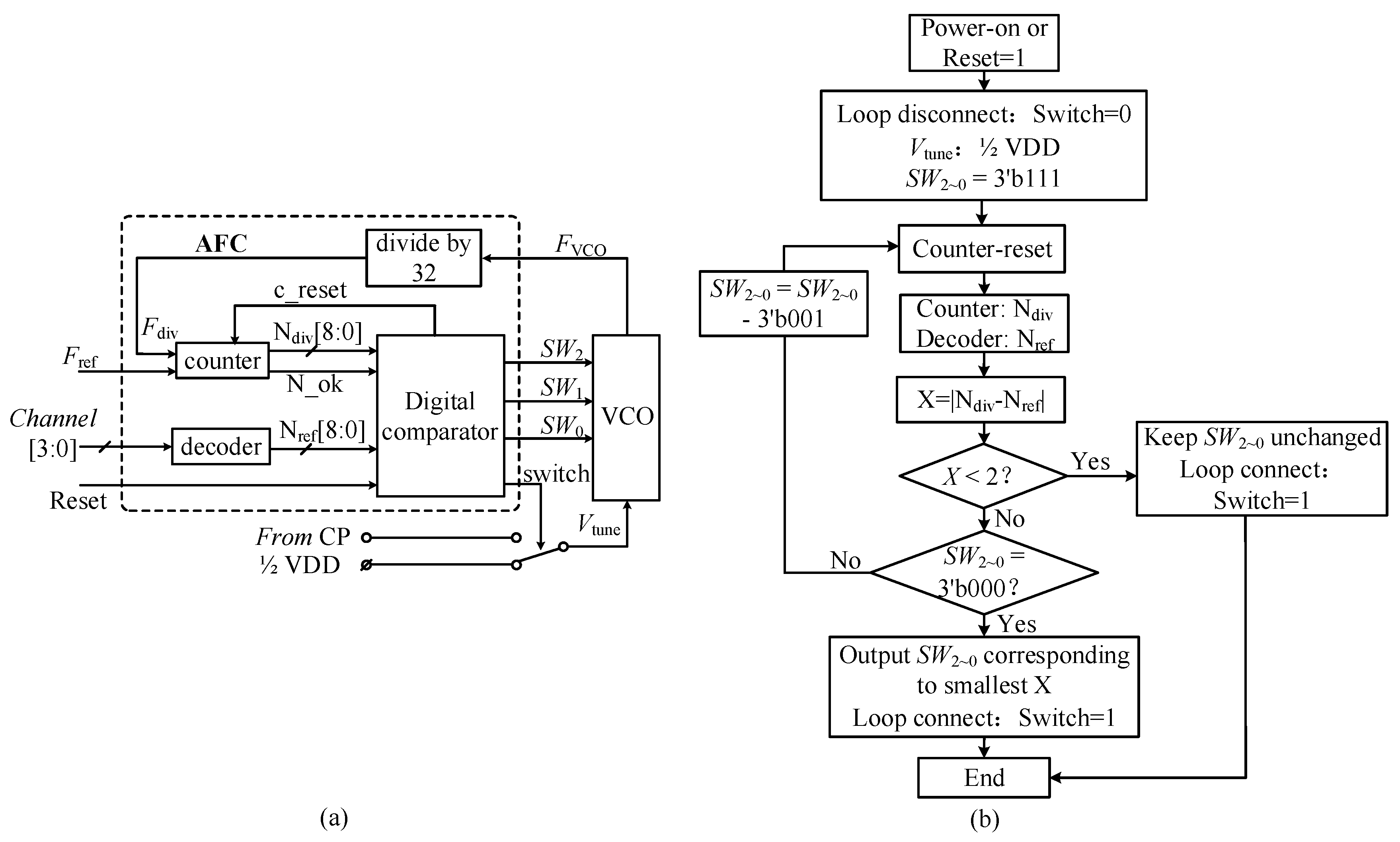
3.1. Implementation of Two-Point Modulation Frequency Synthesizer
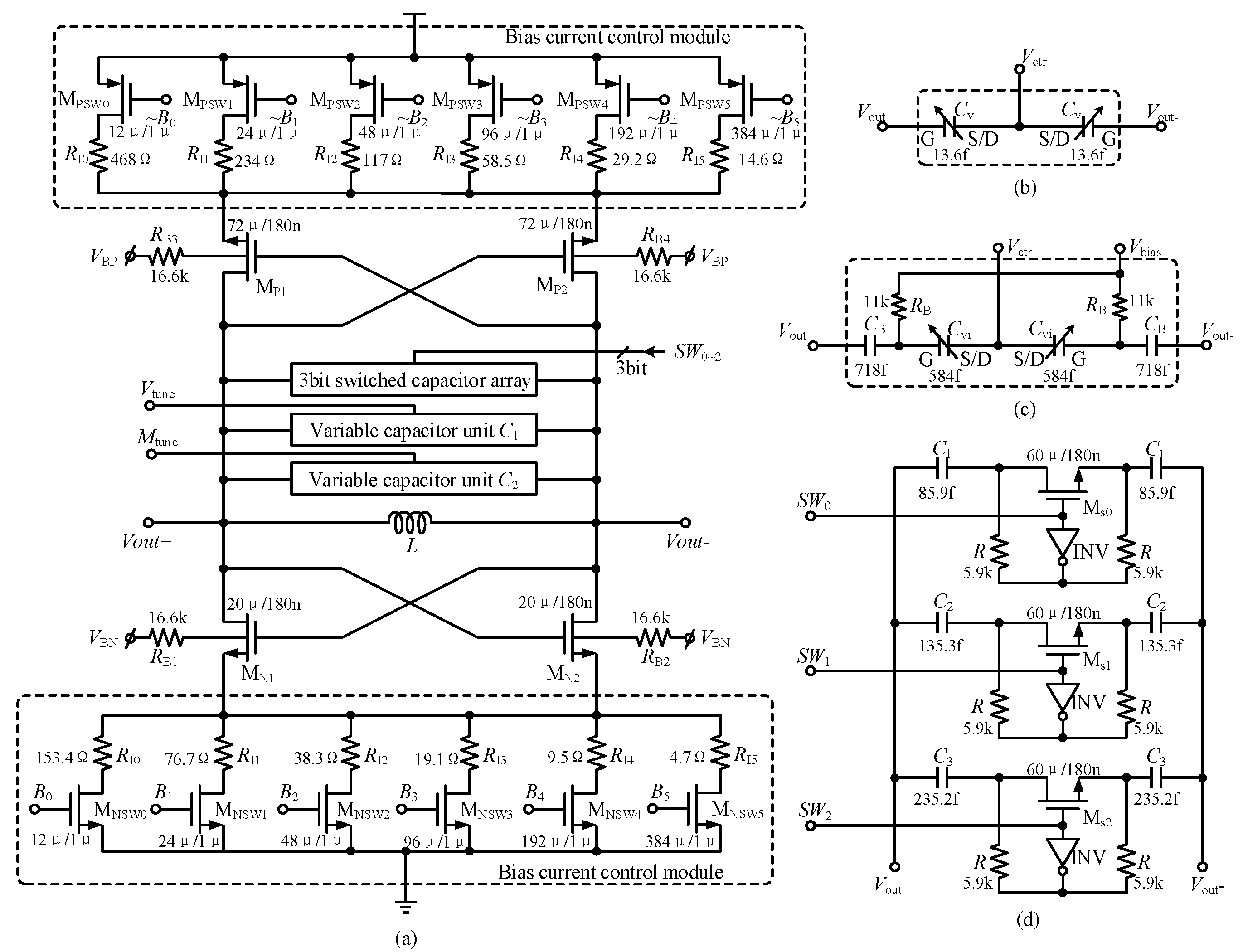
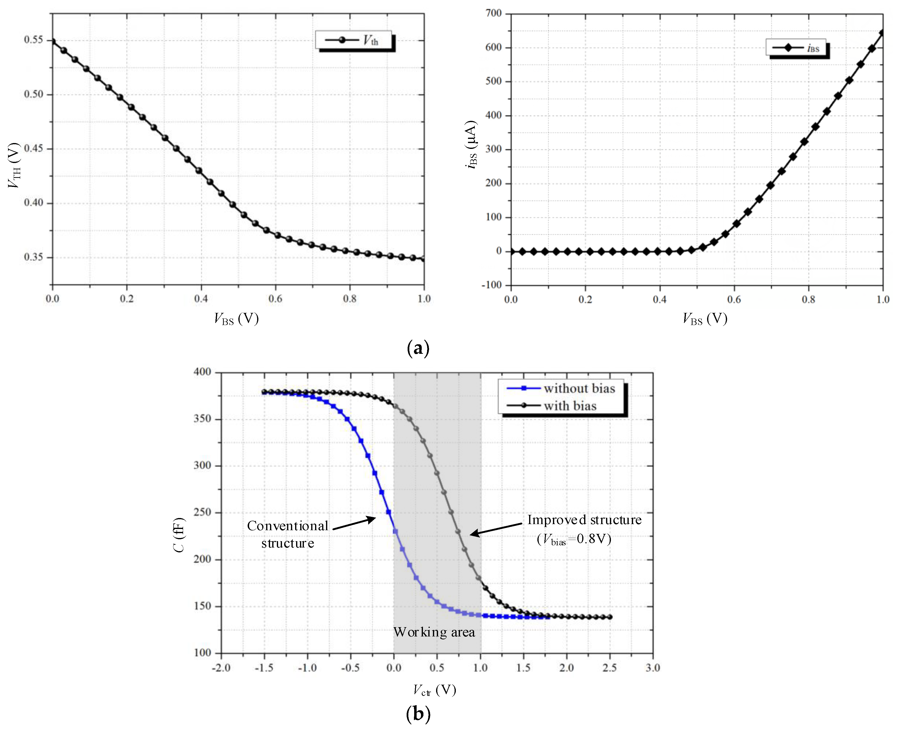
3.2. VCO
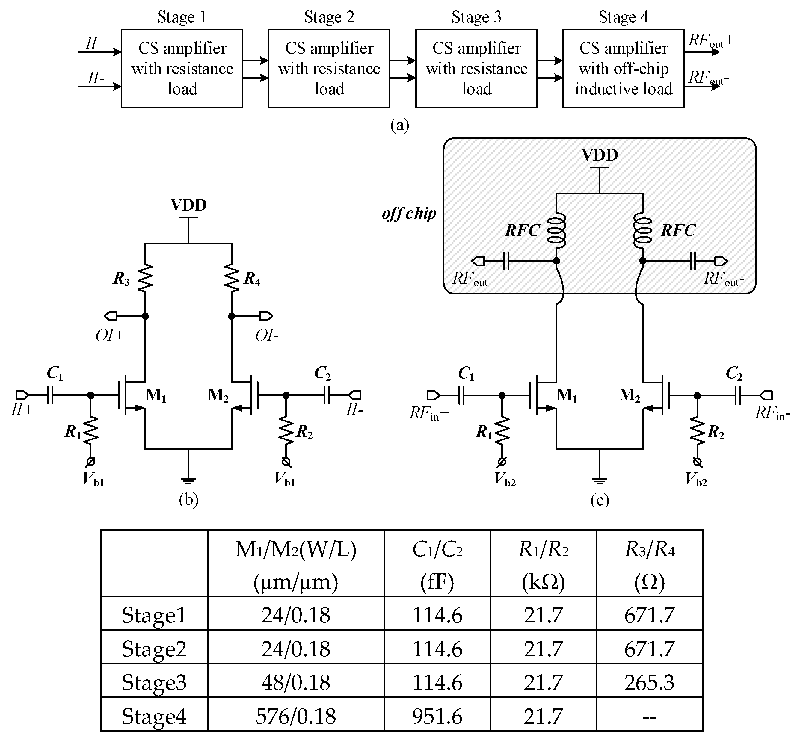
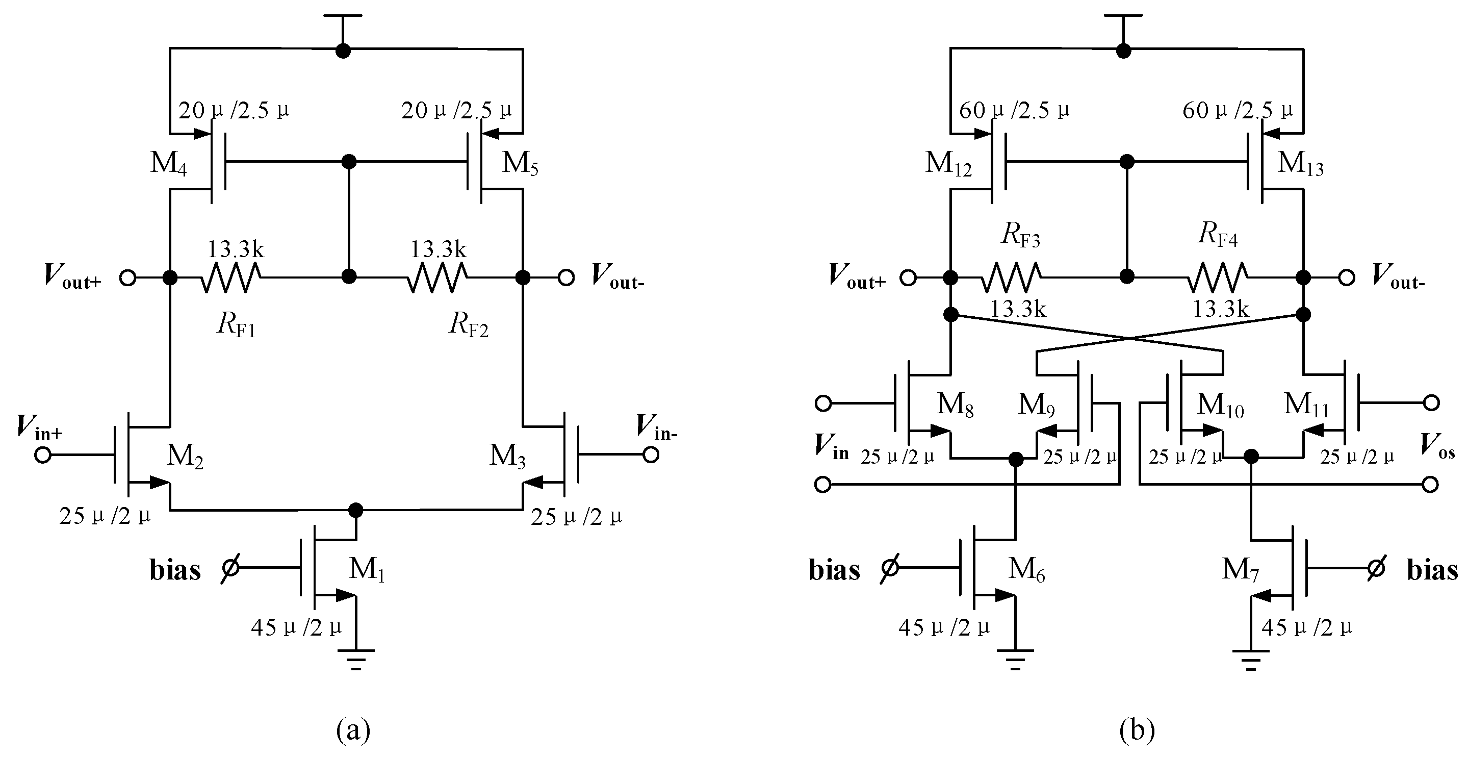
3.3. PA
4. Receiver Design
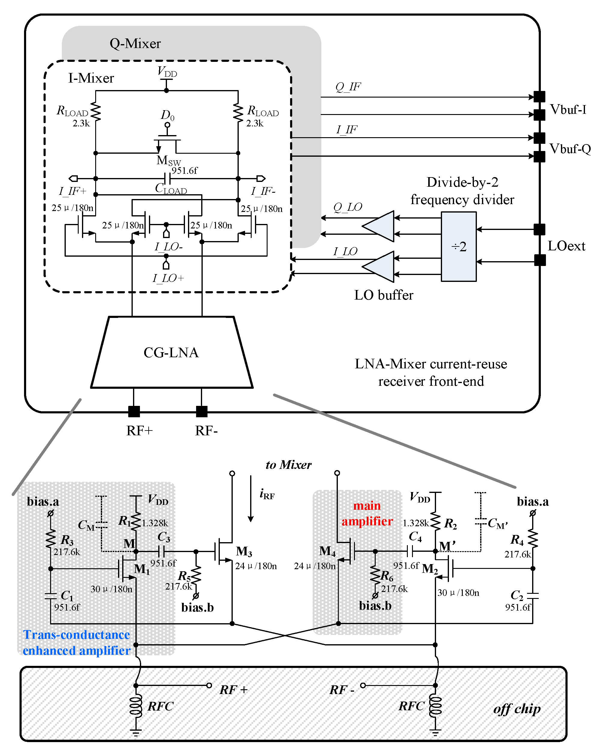
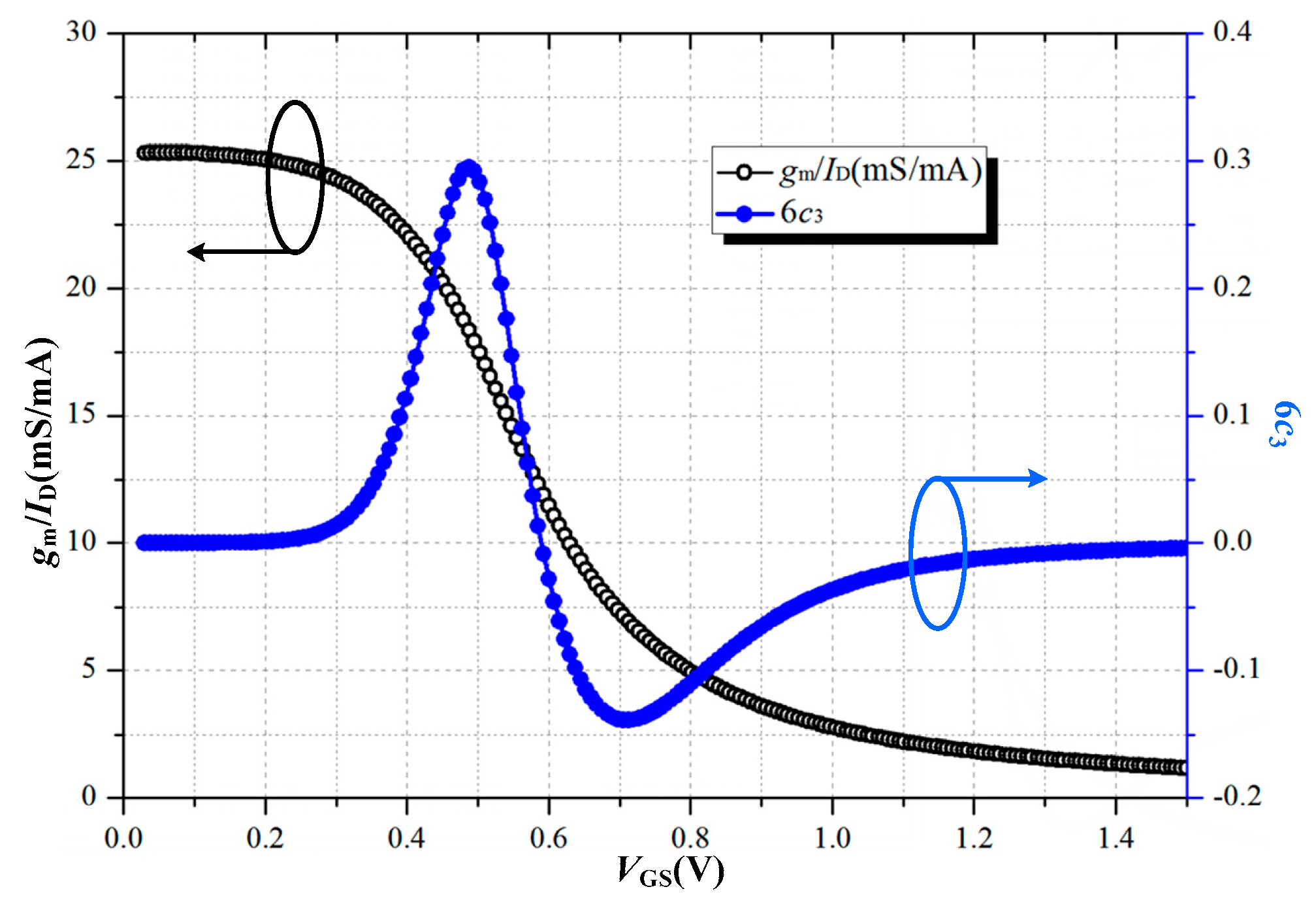
4.1. Receiver Front End
4.2. Complex Band-Pass Filter
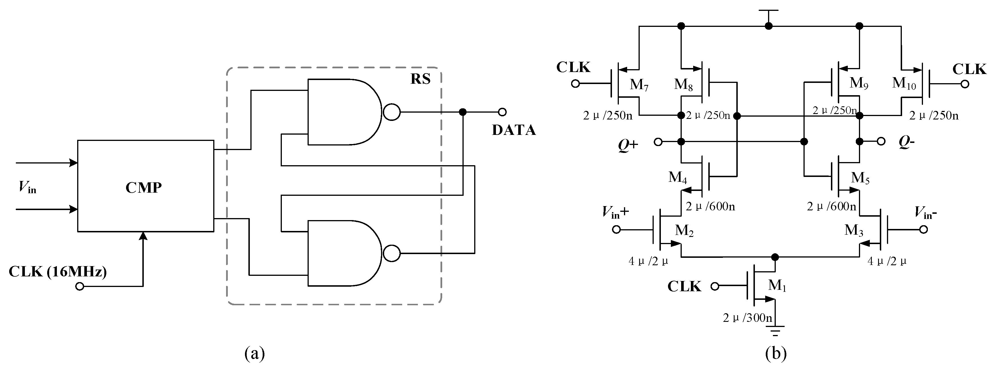
4.3. Modulator
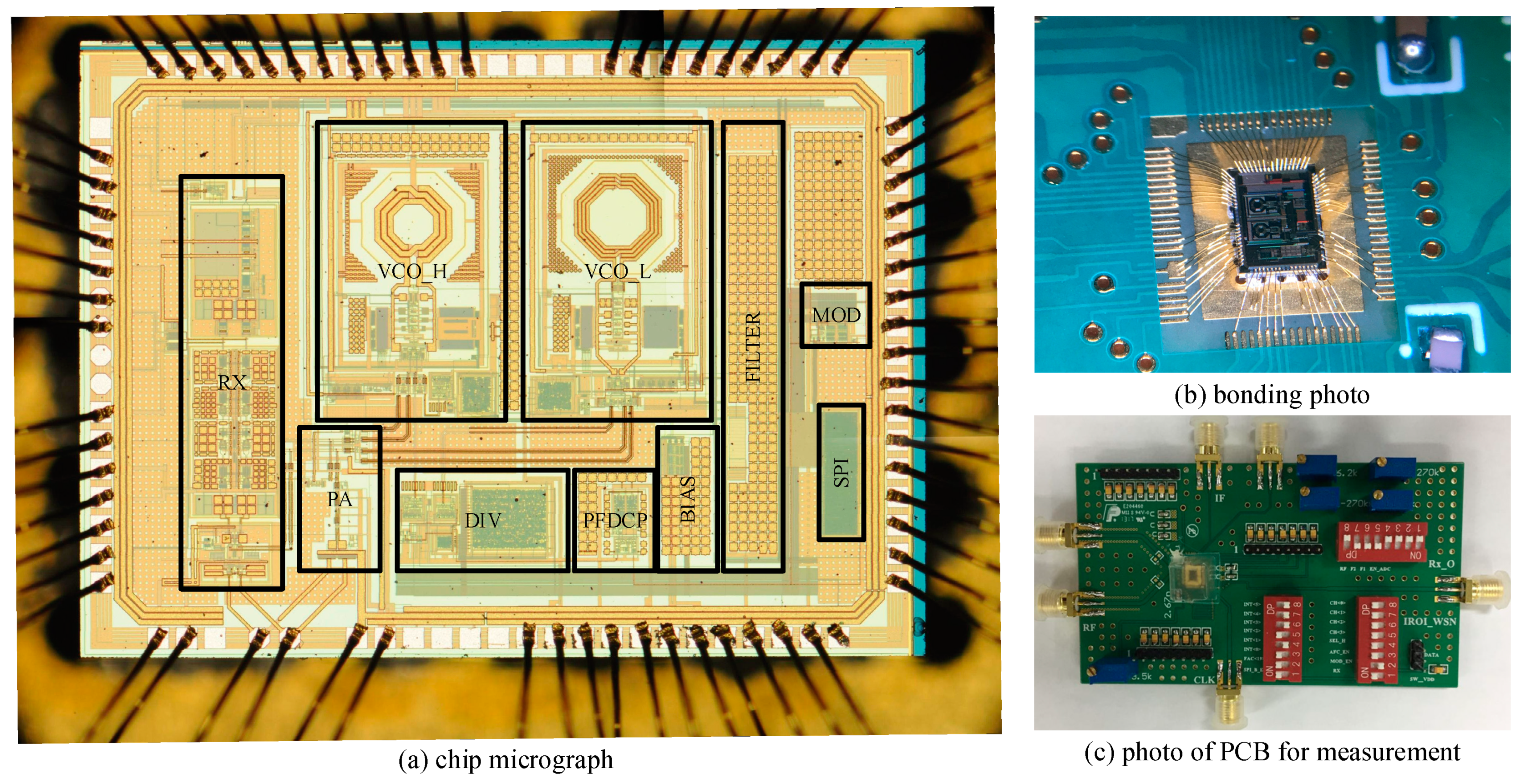
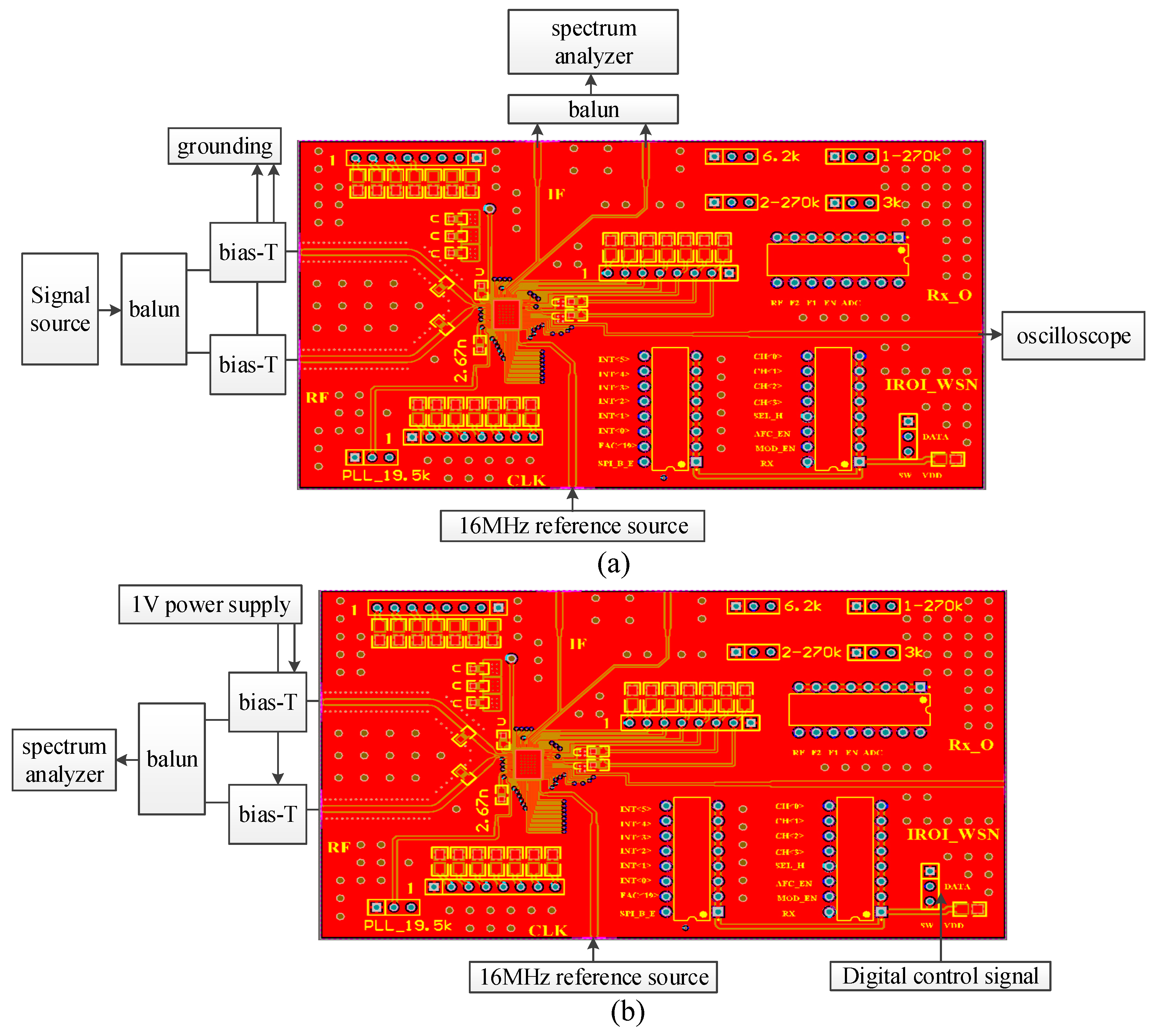
5. Measurement Results
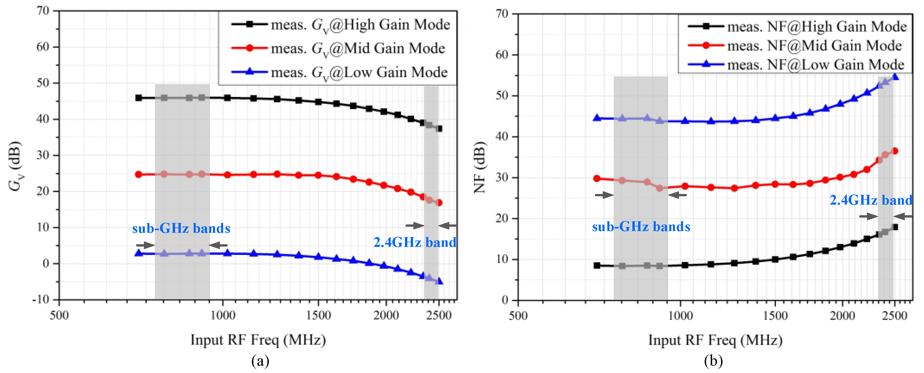
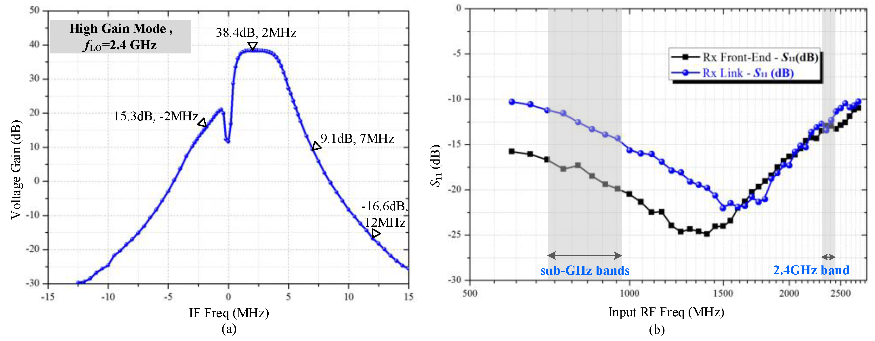
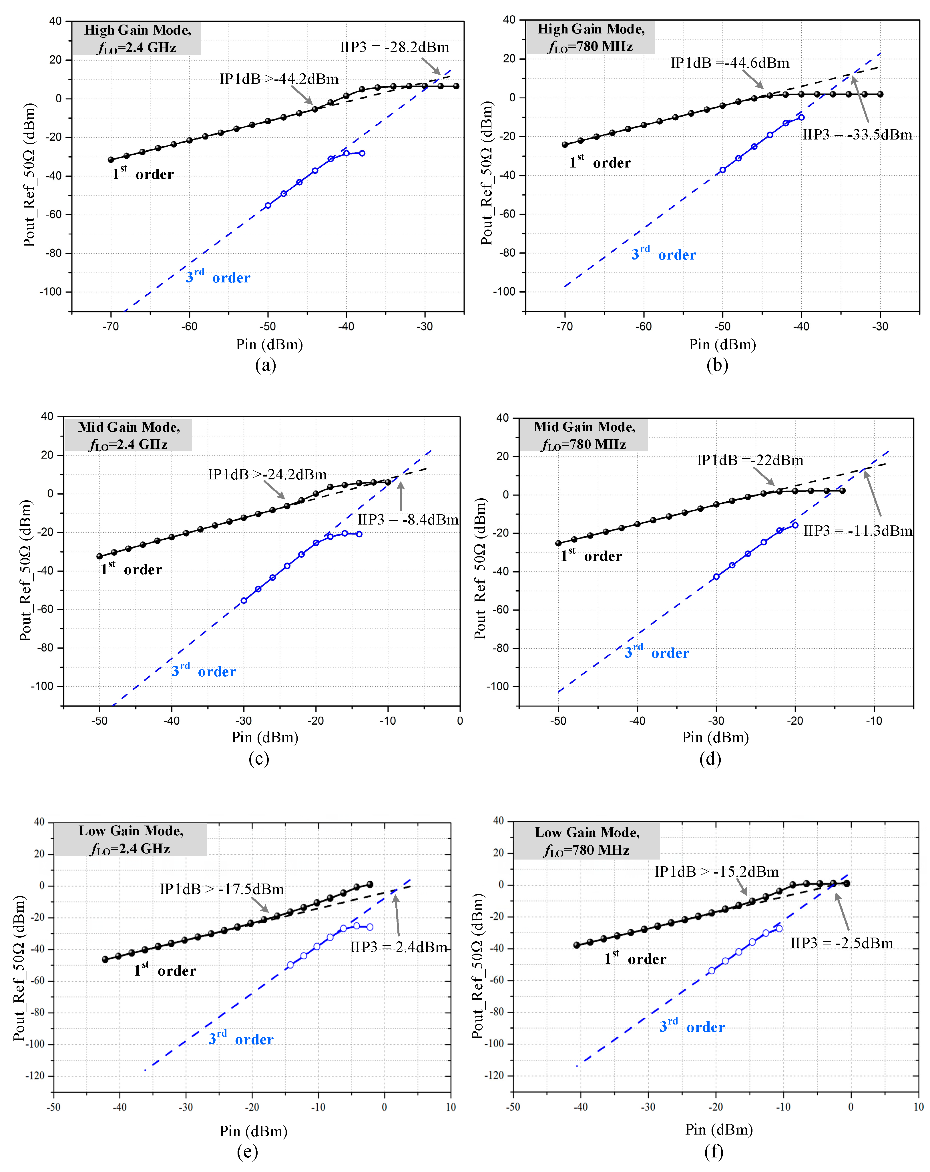
5.1. RX Transmission
5.2. Frequency Synthesizer
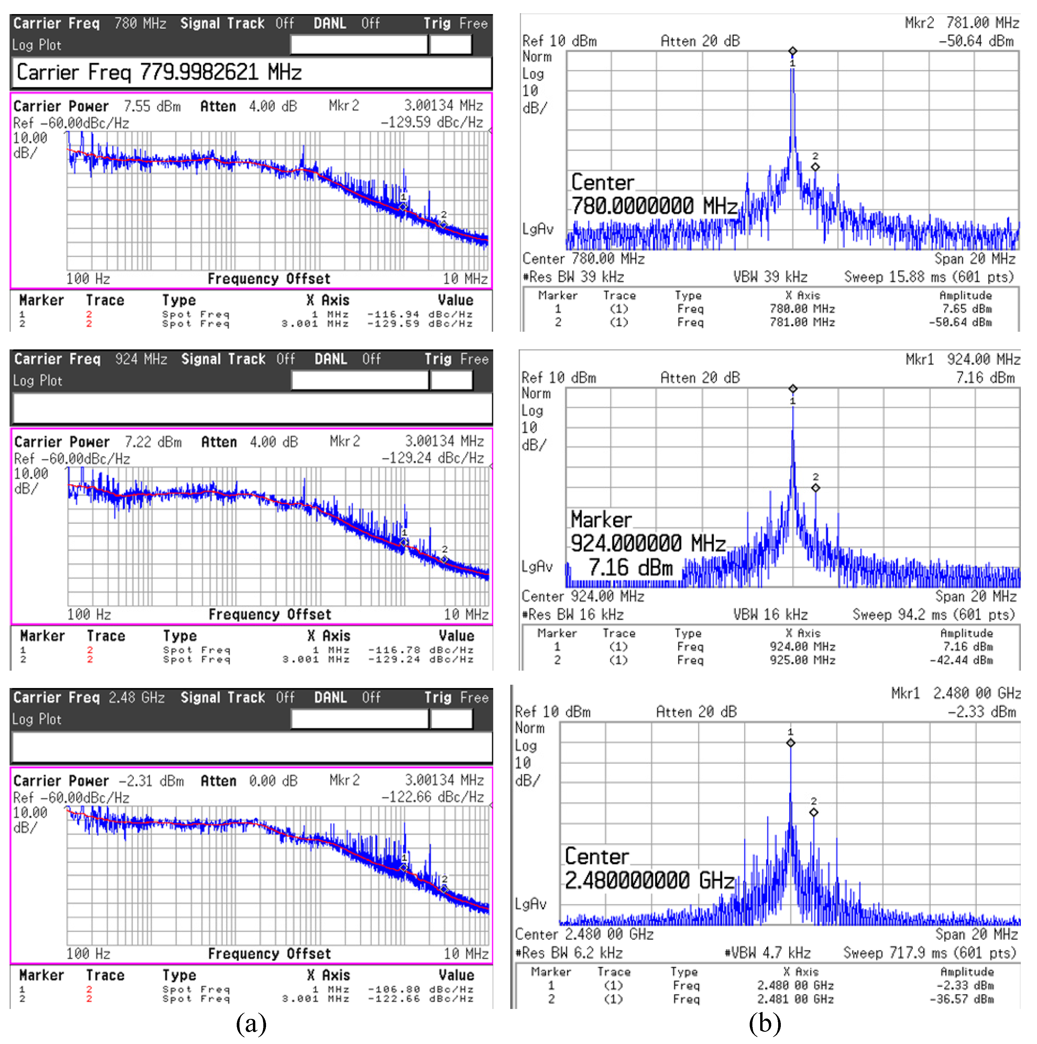
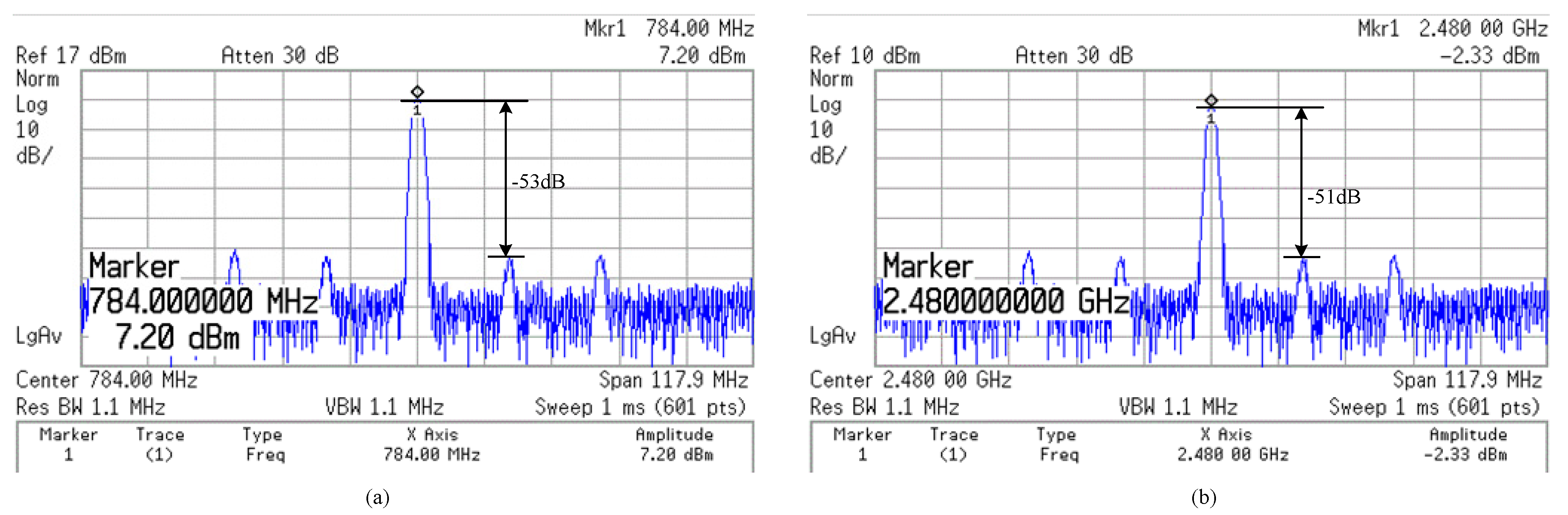
5.3. TX Transmission
5.4. Performance Summary and Comparison
6. Conclusions
Author Contributions
Funding
Acknowledgments
Conflicts of Interest
References
- Cook, B.W.; Berny, A.; Molnar, A.; Lanzisera, S.; Pister, K.S. Low-Power 2.4-GHz Transceiver with Passive RX Front-End and 400-mV Supply. IEEE J. Solid State Circuits 2006, 41, 2757–2766. [Google Scholar] [CrossRef]
- Fiorelli, R.; Villegas, A.; Peralias, E.; Vazquez, D.; Rueda, A. 2.4-GHz single-ended input low-power low-voltage active front-end for ZigBee applications in 90 nm CMOS. In Proceedings of the 20th European Conference on Circuit Theory and Design, Linkoping, Sweden, 29–31 August 2011; pp. 829–832. [Google Scholar] [CrossRef]
- Lee, S.; Jeong, D.; Kim, B. Ultralow-Power 2.4-GHz Receiver with All Passive Sliding-IF Mixer. IEEE Trans. Microw. Theory Tech. 2018, 66, 2356–2362. [Google Scholar] [CrossRef]
- Sayilir, S.; Loke, W.; Lee, J.; Diamond, H.; Epstein, B.; Phodes, D.L.; Jung, B. A—90 dBm Sensitivity Wireless Transceiver Using VCO-PA-LNA-Switch-Modulator Co-Design for Low Power Insect-Based Wireless Sensor Networks. IEEE J. Solid State Circuits 2014, 49, 996–1006. [Google Scholar] [CrossRef]
- Kim, S.J.; Park, C.S.; Lee, S. A 2.4-GHz Ternary Sequence Spread Spectrum OOK Transceiver for Reliable and Ultra-Low Power Sensor Network Applications. IEEE Trans. Circuits Syst. I Regul. Pap. 2017, 64, 2976–2987. [Google Scholar] [CrossRef]
- Kim, S.J.; Lee, D.; Lee, K.; Lee, S. A 2.4-GHz Super-Regenerative Transceiver with Selectivity-Improving Dual Q-Enhancement Architecture and 102-μW All-Digital FLL. IEEE Trans. Microw. Theory Tech. 2017, 65, 3287–3298. [Google Scholar] [CrossRef]
- Lin, Z.; Mak, P.I.; Martins, R.P. A 0.14-mm2 1.4mW 59.4dB SFDR 2.4GHz ZigBee/WPAN Receiver Exploiting a “Split-LNTA+50% LO” Topology in 65nm CMOS. IEEE Trans. Microw. Theory Tech. 2014, 62, 1525–1534. [Google Scholar] [CrossRef]
- Kargaran, E.; Manstretta, D.; Castello, R. Design and Analysis of 2.4 GHz 30 μW CMOS LNAs for Wearable WSN Applications. IEEE Trans. Circuits Syst. I Regul. Pap. 2018, 65, 891–903. [Google Scholar] [CrossRef]
- Sharma, J.; Krishnaswamy, H. A 2.4-GHz Reference-Sampling Phase-Locked Loop That Simultaneously Achieves Low-Noise and Low-Spur Performance. IEEE J. Solid State Circuits 2019, 54, 1407–1424. [Google Scholar] [CrossRef]
- Hsieh, C.; Liu, S. A 2.4-GHz Frequency-Drift-Compensated Phase-Locked Loop with 2.43 ppm/°C Temperature Coefficient. IEEE Trans. Very Large Scale Integr. Syst. 2019, 27, 501–510. [Google Scholar] [CrossRef]
- Xu, Y.; Moon, U. Charge-domain switched-gm-C CBPF using semi-passive charge-sharing technique. Electron. Lett. 2016, 52, 1667–1669. [Google Scholar] [CrossRef]
- Bhuiyan, M.; Badal, M.T.I.; Reaz, M.B.I.; Crespo, M.; Cicuttin, A. Design Architectures of the CMOS Power Amplifier for 2.4 GHz ISM Band Applications: An Overview. Electronics 2019, 8, 477. [Google Scholar] [CrossRef]
- Kluge, W.; Poegel, F.; Roller, H.; Lange, M.; Ferchland, T.; Dathe, L.; Eggert, D. A Fully Integrated 2.4GHz IEEE 802.15.4 Compliant Transceiver for ZigBee Applications. IEEE Int. Solid State Circuits Conf. Dig. Tech. Pap. 2006, 1470–1479. [Google Scholar] [CrossRef]
- Kwon, Y.I.; Park, S.G.; Park, T.J.; Cho, K.S.; Lee, H.Y. An Ultra-Low-Power CMOS Transceiver Using Various Low-Power Techniques for LR-WPAN Applications. IEEE Trans. Circuits Syst. I Regul. Pap. 2012, 59, 324–336. [Google Scholar] [CrossRef]
- Gil, J.; Kim, J.H.; Kim, C.S.; Park, C.; Park, J.; Park, H.; Lee, H.; Lee, S.J.; Jang, Y.H.; Koo, M.; et al. A Fully Integrated Low-Power High-Coexistence 2.4-GHz ZigBee Transceiver for Biomedical and Healthcare Applications. IEEE Trans. Microw. Theory Tech. 2014, 62, 1879–1889. [Google Scholar] [CrossRef]
- Lin, Z.; Mak, P.; Martins, R.P. A Sub-GHz Multi-ISM-Band ZigBee Receiver Using Function-Reuse and Gain-Boosted N-Path Techniques for IoT Applications. IEEE J. Solid State Circuits 2014, 49, 2990–3004. [Google Scholar] [CrossRef]
- Kim, E.H.; Kang, H.; Pyo, C.S.; Kim, C. A CMOS single-chip transceiver design for 700/800/900MHz wireless sensor network applications. In Proceedings of the 2014 International Conference on Information and Communication Technology Convergence (ICTC), Busan, Korea, 22–24 October 2014; pp. 699–700. [Google Scholar] [CrossRef]
- Zhang, L.; Jiang, H.; Wei, J.; Dong, J.; Li, F.; Li, W.; Gao, J.; Cui, J.; Chi, B.; Zhang, C.; et al. A Reconfigurable Sliding-IF Transceiver for 400 MHz/2.4 GHz IEEE 802.15.6/ZigBee WBAN Hubs with Only 21% Tuning Range VCO. IEEE J. Solid State Circuits 2013, 48, 2705–2716. [Google Scholar] [CrossRef]
- Ghahramani, M.M.; Ferriss, M.A.; Flynn, M.P. A 2.4GHz 2Mb/s digital PLL-based transmitter for 802.15.4 in 130nm CMOS. In Proceedings of the 2011 IEEE Radio Frequency Integrated Circuits Symposium, Baltimore, MD, USA, 5–7 June 2011; pp. 1–4. [Google Scholar] [CrossRef]
- IEEE Computer Society. IEEE Std 802.15.4: Wireless Medium Access Control (MAC) and Physical Layer (PHY) Specifications for Low-Rare Wireless Personal Area Networks (WPANs); IEEE Press: New York, NY, USA, 2006. [Google Scholar]
- Razavi, B. RF Microelectronics; Prentice Hall PTR: Englewood Cliffs, NJ, USA, 1998. [Google Scholar]
- Oh, N.J.; Lee, S.G. Building a 2.4-GHZ radio transceiver using IEEE 802.15.4. IEEE Circuits Devices Mag. 2006, 21, 43–51. [Google Scholar] [CrossRef]
- Richard, C.L. RF Circuit Design; Prentice Hall PTR: Hoboken, NJ, USA, 2009; pp. 764–766. [Google Scholar]
- Li, X.; Shekhar, S.; Allstot, D.J. Gm-boosted common-gate LNA and differential colpitts VCO/QVCO in 0.18-/spl mu/m CMOS. IEEE J. Solid State Circuits 2005, 40, 2609–2619. [Google Scholar] [CrossRef]
- Li, Z.; Wang, Z.; Zhang, M.; Chen, L.; Wu, C.; Wang, Z. A 2.4 GHz ultra-low-power current-reuse CG-LNA with Active Gm-boosting technique. IEEE Microw. Wirel. Compon. Lett. 2014, 24, 348–350. [Google Scholar] [CrossRef]
- Comer, D.J.; Comer, D.T. Operation of analog MOS circuits in the weak or moderate inversion region. IEEE Trans. Educ. 2004, 47, 430–435. [Google Scholar] [CrossRef]
- Maxim Integrated Three Methods of Noise Figure Measurement. Available online: https://www.maximintegrated.com/en/design/technical-documents/tutorials/2/2875.html (accessed on 28 November 2019).
- MICROCHIP. MRF24J40MA Data Sheet. Available online: https://www.microchip.com/wwwproducts/en/en535967 (accessed on 29 November 2019).
- ANALOG DEVICES. ADF7242 Data Sheet. Available online: https://www.analog.com/media/en/technical-documentation/data-sheets/ADF7242.pdf (accessed on 29 November 2019).
- ANALOG DEVICES. ADF7023 Data Sheet. Available online: https://www.analog.com/media/en/technical-documentation/data-sheets/ADF7023.pdf (accessed on 29 November 2019).


| Frequency Band (MHz) | Modulation Mode | Chip Rate Fchip (Mchip/s) | Center Frequency fC (MHz) |
|---|---|---|---|
| 780 | O-QPSK | 1 | 780 + 2k, k = 0, …, 3 |
| 868 | O-QPSK | 0.4 | 868.3 |
| 915 | O-QPSK | 1 | 906 + 2k, k = 0, …, 9 |
| 2400 | O-QPSK | 2 | 2405 + 5k, k = 0, …, 15 |
| Index | Input Signal Ranges (dBm) | NF (dB) | IIP3 (dBm) |
|---|---|---|---|
| Low gain level | −35~−20 | -- | >−10 |
| Mid gain level | −60~−35 | <45.5 | -- |
| High gain level | −85~−60 | <20.5 | >−34.25 |
| Channel [3:0] | Locked SW2~0 | Output Frequency Divided by 2/MHz | Channel Center Frequency/MHz | Frequency Deviation/MHz |
|---|---|---|---|---|
| 4′b0000 | 3′b101 | 2413 | 2405 | 8 |
| 4′b0001 | 3′b101 | 2413 | 2410 | 3 |
| 4′b0010 | 3′b101 | 2413 | 2415 | 2 |
| 4′b0011 | 3′b101 | 2413 | 2420 | 7 |
| 4′b0100 | 3′b101 | 2413 | 2425 | 12 |
| 4′b0101 | 3′b101 | 2413 | 2430 | 17 |
| 4′b0110 | 3′b101 | 2413 | 2435 | 22 |
| 4′b0111 | 3′b101 | 2413 | 2440 | 27 |
| 4′b1000 | 3′b101 | 2413 | 2445 | 32 |
| 4′b1001 | 3′b100 | 2481 | 2450 | 31 |
| 4′b1010 | 3′b100 | 2481 | 2455 | 26 |
| 4′b1011 | 3′b100 | 2481 | 2460 | 21 |
| 4′b1100 | 3′b100 | 2481 | 2465 | 16 |
| 4′b1101 | 3′b100 | 2481 | 2470 | 11 |
| 4′b1110 | 3′b100 | 2481 | 2475 | 6 |
| 4′b1111 | 3′b100 | 2481 | 2480 | 1 |
| Frequency Band (MHz) | Gain Mode | Conversion Gain (dB) | NF (dB) | IIP3 (dBm) |
|---|---|---|---|---|
| 780 | High | 45.9 | 8.4 | −33.5 |
| Mid | 24.8 | 29.3 | −11.3 | |
| Low | 2.7 | 44.4 | −2.5 | |
| 868 | High | 45.9 | 8.5 | --- |
| Mid | 24.7 | 28.9 | --- | |
| Low | 2.8 | 44.5 | --- | |
| 915 | High | 46.0 | 8.4 | --- |
| Mid | 24.8 | 27.4 | --- | |
| Low | 2.8 | 43.8 | --- | |
| 2400 | High | 38.4 | 16.7 | −28.2 |
| Mid | 17.6 | 35.6 | −8.4 | |
| Low | −4.1 | 53.3 | 2.4 |
| Channel Frequency (MHz) | Output Power (dBm) | Current Consumption (mA) | |||
|---|---|---|---|---|---|
| PA | Frequency Synthesizer | Modulator | Total | ||
| 780 | 12.65 | 65 | 3.5 | 1 | 69.5 |
| 868 | 12.37 | 65 | 3.5 | 1 | 69.5 |
| 924 | 12.16 | 65 | 3.5 | 1 | 69.5 |
| 2480 | 2.67 | 16 | 4.2 | 1 | 21.2 |
| This Work | [14] | [15] | [16] | [28] | [29] | [30] | Unit | ||
|---|---|---|---|---|---|---|---|---|---|
| RF frequency range | 700–1000 | 2400–2500 | 2405–2480 | 2405–2480 | 433–960 | 2405–2480 | 2400–2483.5 | 862–928 | MHz |
| TX output power | 12.65 | 2.67 | 5 | 9 | -- | 0 | 3 | 10 | dBm |
| Phase Noise | −107 | -- | dBc/Hz | ||||||
| @1MHz offset | −116.7 | −106.8 | −111.5 | -- | −135f | −126 | |||
| @3MHz offset | −129.2 | −122.6 | -- | −117.4d | −145g | −131 | |||
| RX Conversion Gain | 45.9a | 38.4a | 102.5 | -- | 50 | -- | -- | -- | dB |
| 24.7b | 17.6b | ||||||||
| 2.7c | −4.1c | ||||||||
| RX Sensitivity | −102 | −93.8 | −101 | −97 | -- | −94 | −95 | −100 | dBm |
| RX NF | 8.5a | 16.7a | 6.2 | 7.5 | 8.1 | 8 | -- | -- | dB |
| 29.3b | 35.6b | ||||||||
| 44.5c | 53.3c | ||||||||
| RX IIP3 | −33.5a | −28.2a | −11 | -- | −20.5 | -- | −13.6 | −12.2 | dBm |
| −11.3b | −8.4b | ||||||||
| −2.5c | 2.4c | ||||||||
| Channel Rejection | -- | -- | -- | dB | |||||
| Image | 23.1 | - | -- | 36 | |||||
| Adjacent (±5 MHz) | 29.3 | 30.9 | 30 | 38 | |||||
| Alternate (±10 MHz) | 55 | 52 | 40 | -- | |||||
| Current Consumption | mA | ||||||||
| RX mode | 4.92 | 5.62 | 14.3 | 15.4 | 2.3 | 19 | 19 | 12.8 | |
| TX mode | 69.5 | 21.2 | 16.7 | 28.4 | -- | 23 | 21.5 | 24.1 | |
| Supply voltage | 1 | 1.8 | 1.2 | 0.5 | 3.3 | 3.6 | 3 | V | |
| Technology | 180 | 180 | 90 | 65 | -- | -- | -- | nm | |
| Die Size | 6.04 | 7.84 | 3.24 | 0.2 | 496.6e | 25h | 25h | mm2 | |
© 2019 by the authors. Licensee MDPI, Basel, Switzerland. This article is an open access article distributed under the terms and conditions of the Creative Commons Attribution (CC BY) license (http://creativecommons.org/licenses/by/4.0/).
Share and Cite
Li, Z.; Yao, Y.; Wang, Z.; Cheng, G.; Luo, L. A Low-Voltage Multi-Band ZigBee Transceiver. Electronics 2019, 8, 1474. https://doi.org/10.3390/electronics8121474
Li Z, Yao Y, Wang Z, Cheng G, Luo L. A Low-Voltage Multi-Band ZigBee Transceiver. Electronics. 2019; 8(12):1474. https://doi.org/10.3390/electronics8121474
Chicago/Turabian StyleLi, Zhiqun, Yan Yao, Zengqi Wang, Guoxiao Cheng, and Lei Luo. 2019. "A Low-Voltage Multi-Band ZigBee Transceiver" Electronics 8, no. 12: 1474. https://doi.org/10.3390/electronics8121474
APA StyleLi, Z., Yao, Y., Wang, Z., Cheng, G., & Luo, L. (2019). A Low-Voltage Multi-Band ZigBee Transceiver. Electronics, 8(12), 1474. https://doi.org/10.3390/electronics8121474