Article

Development and Implementation of a Low Cost μC- Based Brushless DC Motor Sensorless Controller: A Practical Analysis of Hardware and Software Aspects

by
Yannis L. Karnavas
1,
Anestis S. Topalidis
1 and
Maria Drakaki
2,*
1
Electrical Machines Laboratory, Department of Electrical & Computer Engineering, Democritus University of Thrace, 67100 Xanthi, Greece
2
Department of Industrial Engineering & Management, International Hellenic University, 57400 Thessaloniki, Greece
*
Author to whom correspondence should be addressed.
Electronics 2019, 8(12), 1456; https://doi.org/10.3390/electronics8121456
Submission received: 23 October 2019 / Revised: 25 November 2019 / Accepted: 29 November 2019 / Published: 1 December 2019
(This article belongs to the Section Systems & Control Engineering)

Abstract

:
The ongoing technological advancements of brushless DC motors (BLDCMs) have found a wide range of applications. For instance, ground-based electric vehicles, aerial drones and underwater scooters have already adopted high-performance BLDCMs. Nevertheless their adoption demands control systems to monitor torque, speed and other performance characteristics. Precise design structure and the particular motor functional characteristics are essential for the suitable configuration and implementation of an appropriate controller to suit a wide range of applications. Techniques which do not use Hall sensors should be used then. This paper deals with the analysis of hardware and software aspects during the development of such a microcontroller based and low cost speed controller for motors up to 500 W, along with its practical implementation. The sensorless method employed is based on the zero crossing point (ZCP) detection of the back-electromotive forces’ (back-EMF) differences, as the ZCPs of these quantities match to the time points at which the commutation sequence changes. Additionally, the study presents hardware and software details through calculations, figures, flowcharts and code, providing an insight of the practical issues that may arise in such a low cost prototype. Finally, results obtained by experiments validate the presented hardware/software architecture of the controller.

1. Introduction

The availability and the low cost of high energy density permanent magnets made of rare earth materials, has resulted during the last decades in the development of electrical machines which rely on magnets for the creation of the excitation field instead of excitation windings that carry currents. Thus, permanent magnet synchronous motors (PMSMs) were adopted, along with their subclass, namely the brushless direct current motors (BLDCMs). Additionally, in the recent years there has been a rapid increase in the demand for electrification in modern drive-trains. Electric motors have been utilized so far in almost all the forms of vehicle applications, either in purely electrical or in hybrid setups. Until recently, conventional direct current motors (CDCMs), e.g., permanent magnet DC motors, were the only type of motor used, mostly in car applications. On the other hand, BLDCMs seem to have become the dominant type of motors nowadays in any type of electrified vehicle. This can be justified easily though, since they exhibit higher efficiency levels, higher power density characteristics, higher torque/weight ratio and inherently better operational flexibility compared to their CDCM counterparts. Consequently, BLDCMs may nowadays be used in various application areas such as industrial automation, medical, automotive, hand-held equipment, among others [1]. As the name of these motors implies, electronic switching of current through their stator windings, is done by using semiconductor elements in suitable inverter topologies instead of mechanical switching (i.e., by commutator/brushes apparatus) as in CDCMs. Actually, BLDCMs belong to the category of “reverse” DC motors, because both the windings of the excitation field and the armature winding were transferred from the rotor to the stator and vice versa [2].
Yet the motors are controlled by inverters which necessitate the use of a rotor position sensor for the correct switching sequence in the windings of the stator both in starting stage and during operation [2]. A sensor control system however has the disadvantage in that it increases the motor cost and its size. Moreover, in order to mount the sensors a special mechanical arrangement is used. Additionally, these sensors show sensitivity to high temperatures; therefore limiting the operation of the motors to less than 75 °C. Moreover, the reliability of the driving system is reduced since the sensors operate in a dusty environment [3,4]. Therefore, the above reasons in recent years have drawn attention to sensorless control [5,6]. The construction of sensor-free motor is thus simplified by reducing costs. Obviously, the overall reliability of the drive with such a driving system comprised of fewer components is higher. At the same time, there is always a need of fast, reliable and low cost sensorless controllers along with their operational techniques to be developed and support this kind of motor scheme.
The most common sensorless method employed in the majority of the studies, is the back-EMF method, which is by far the most mature, effective widely used method of rotor position detection. It includes three main methods: zero crossing point (ZCP) method, phase-lock loop method and integration method. The term back-EMF method usually refers to the ZCP method [7]. Direct back-EMF control strategies have presented in [8,9], yet these methods suffer from poor, low-speed performance and require filters to suppress high frequency noise, which may induce large phase shifts to the commutation signals at high speed. Meanwhile, the terminal voltage distortion caused by the diode freewheeling current can make the position detection signal phase advance, deviating from the ideal commutation instant, especially in heavy-load conditions [10]. A new back-EMF difference estimation method was proposed in [11], while in [12] an approach utilizing averaged line-to-line voltages with simple RC circuits and comparators was demonstrated. A control strategy using one-cycle current have been employed in [13] towards improved dynamic behavior. Also, an unbalanced ZCP were considered in [14] and a compensation method was proposed for sensorless position estimation. Sliding mode control for recovery on disturbance interference during motor operation has also recently presented in [15]. Then problem of smooth operation of sensorless BLDCM from stand still o high speed conditions has been addressed in [16,17]. Other problem faced during these motors operation include torque ripple minimization (which is an inherent operational feature) and several commutation techniques have also been proposed e.g., [18,19,20].
Additionally, many efforts in BLDCM sensorless controller development have been conducted and introduced in the recent literature, either by use of simulation such as [21,22,23], or in experimental form, e.g., [9,24,25]. The former approaches, although useful to prove the conceptual design, are far from real operation, whereas in the latter, the fact is that most of these studies employ ready-made solutions like FPGA development, expensive industrial controllers, etc, which are not very convenient either in hardware or software parameterization in prototyping terms.
Generally speaking, in some applications where the controller itself is not of actual interest, a readymade one may be purchased and used, depending on its characteristics and cost, but there are many situations where a custom, low cost and fully parameterized prototype should be built. In this case, practical difficulties may arise concerning either in hardware or in software level.
Based on this consideration, the main contributions of the paper are: (a) to present a simple but complete practical reference when similar low-cost BLDCM controllers are to be considered, (b) to present the relevant details in the required hardware of such a system, (c) to clarify the required interconnections between the different stages of the controller and (d) to propose a simple but effective control strategy accompanied by the corresponding software source code. It is to be noted that similar efforts providing as a single document an extended degree of technical completeness, as the one presented here are not found in the scientific literature.
In the above context, the paper presents a straightforward practical implementation approach of a low-cost BLDCM sensorless controller system. Having the simplicity and the low cost as a priority, several issues regarding the hardware selection are discussed and discrete components selection is commented. Detailed schematics of the proposed architecture clarify the overall scheme. Moreover, the corresponding control strategy adopted is given thoroughly, based on the simplicity and portability. Additionally, the relative microcontroller source code is presented. Based on suitable components and microcontroller architectures, another potential feature is the applicability of the proposed controller in harsh environments. The operating environments where this scheme can be applied may cover a wide range of conditions such as ambient temperature. The selected here microcontroller’s manufacturer datasheet, reveals that this limits can be from −40 °C to +85 °C/+125 °C for industrial/extended high temperature environments (storage temperature may vary from −65 °C to +150 °C), which obviously promise satisfactory operation in harsh environments.
Finally, the prototype’s experimental results reveal the degree of goodness and the validity of the procedure followed. The paper is organized as follows: The problem statement and the corresponding theory are given in Section 2. The controller design from a hardware perspective is analyzed in Section 3. The control philosophy is presented in Section 4, whereas software characteristics are highlighted. Indicative experimental results are shown in Section 5. Finally the work concludes in Section 6.

2. Problem Statement and Methods Used

2.1. Brief Theoretical Background of BLDCM Operation

BLDCMs develop torque with the aid of two magnetic fields. The induced torque tends to align the fields. Specifically, the torque rotates the rotor in order to align its magnetic field with that of the stator. The torque should become maximum when the two field vectors are perpendicular to each other and tend to zero when they tend to become parallel. Since the motion of the rotor is continuous, the direction of the field created by the stator windings as the rotor moves should be changed, in order that the produced torque does not diminish. Therefore, power supply switching is required [1,2]. At least six switching elements are required to implement this operation for three phases (a four switches one has been examined in [26]), which comprise the so called “inverter bridge” or “six step commutation scheme”. Therefore, the problem focuses on the proper (in terms of sequence) and precise (in terms of timing) pulsing of the switching elements.
In Figure 1 the generic topology of a microcontroller based BLDCM controller scheme is shown, where—among other details—the equivalent circuit of a star-connected BLDCM, as well as the configuration of the inverter are shown. The voltages equations in such a case are given by:
[ v a v b v c ] = R [ i a i b i c ] + L d d t [ i a i b i c ] + [ e a e b e c ]
where va, vb and vc are the stator phase voltages; R is the stator resistance per phase (Ra = Rb = Rc = R); Ia, Ib and Ic are the stator phase (or line) currents; L is the self inductance per phase (La = Lb = Lc = L) and ea, eb and ec are the corresponding back EMFs. The latter can be shown as:
[ e a e b e c ] = K e [ f a ( θ e ) f b ( θ e 2 π / 3 ) f c ( θ e + 2 π / 3 ) ] ω
where Ke is the back-EMF constant in V/rad/s; θe is the electrical rotor angle in electrical degrees (depending on the number of BLDCM poles); ω is the mechanical rotor speed in rad/sec. Therefore, the back-EMF for each phase is a function of rotor position f(θ)and can be expressed as:
f a ( θ e ) = { 6 θ e / π 0 θ e π / 6 + 1 π / 6 θ e 5 π / 6 6 ( π θ e ) / π 5 π / 6 θ e 7 π / 6 1 7 π / 6 θ e 11 π / 6 6 ( θ e 2 π ) / π 11 π / 6 θ e 2 π
Accordingly fbe) and fce) can be calculated [9]. From Equation (1) for each phase we have:
[ v a v b v c ] = [ R 0 0 0 R 0 0 0 R ] [ i a i b i c ] + [ L 0 0 0 L 0 0 0 L ] d d t [ i a i b i c ] + [ e a e b e c ]
However, in practice, the line voltages are used. Thus, by performing suitable calculations Equation (4) is transformed to the following appropriate form:
[ v a b v b c v c a ] = [ R R 0 0 R R R 0 R ] [ i a i b i c ] + [ L L 0 0 L L L 0 L ] d d t [ i a i b i c ] + [ e a b e b c e c a ]
Also, it is known that regarding the currents with respect to the neutral point, the following expression is valid:
i a + i b + i c = 0
By expanding Equation (5) and substituting in Equation (6) we get:
v a b = R ( i a i b ) + L d d t ( i a i b ) + e a b v b c = R ( i b i c ) + L d d t ( i b i c ) + e b c v c a = R ( i c i a ) + L d d t ( i c i a ) + e c a E q . ( 6 ) v a b = R ( i a i b ) + L d d t ( i a i b ) + e a b v b c = R ( i a + 2 i b ) + L d d t ( i a + 2 i b ) + e b c
Finally, solving for current derivatives leads to Equation (8) which is the expression that can be used when the ZCP technique is applied because it can "detect" the time instants when a voltage zero crossing is performed. It is to be noted that only two equations are needed for the voltage differences since the third one (if needed) can be easily derived:
d d t [ i a i b ] = [ R L 0 0 R L ] [ i a i b ] + [ 2 3 L 1 3 L 1 3 L 1 3 L ] [ v a b e a b v b c e b c ]

2.2. Zero-Crossing Points (ZCP) Detection Technique

This is one of the simplest back-EMF detection techniques. It is based on the detection of a time instant when the back-EMF of the non-excited phase becomes zero. Because back-EMF cannot be directly measured, a ZCP is detected through the supply phase voltage, which is identical to the back-EMF during the idle period. By detecting a zero point and providing a 30° phase shift, it is possible to correctly estimate the start of the next switching step and consequently the correct motor driving [27]. This can be done by activating a counter such as the inverter is led to the next switching phase after the measured time has elapsed. In addition, it is necessary to use low-pass filters before detecting the zero point due to the inverter’s power components harmonics introduced. Otherwise, incorrect ZCP detection may occur, which leads to incorrect switching and improper motor operation. To reduce the noise from the inverter power components, PWM configuration is applied to the upper or lower switching devices and zero points are detected during the interruption period. This does not affect the measurement of the interference noise and thus increases the motor performance [8].
The ZCP of the back EMF for each phase could be an attractive feature for sensing, since these points do not depend on the speed and the phase winding is not excited at the rotor positions at which they occur. Yet the ZCP points do not correspond to the commutation points (CPs). Thus, the signals must be shifted in phase by 90° electrical, before they will be used for commutation. In order to overcome the phase-shifting problem different methods have been presented in the literature, including the detection of the third harmonic component in back EMF, direct current control algorithm and phase locked loops [8,12,28,29]. Nevertheless, as stated in [14], BLDC motor systems are typically applied to low-cost systems of small capacity. Therefore, implementation of the ZCP compensation method should be relatively simple.

2.3. Sensorless Method with back EMF Difference Calculation

The method which has been implemented in this paper utilizes the difference in back EMF of two phases instead of using phase back-EMF. The waveform of the back-EMF difference is shown in Figure 2a. Zero points coincide with the time points at which the switching stage changes. Analysis of the equivalent circuit of the motor easily reveals that vba voltage (vb-va difference) give a waveform which crosses zero at the same instant to which the eba voltage (eb-ea difference) waveform crosses zero. Therefore, the vba ZCP coincides with the eba ZCP. Thus, the ZCPs of this waveform can be used to generate the virtual Hall signal for phase B switching. This signal will coincide with the actual Hall B phase signal coming from the sensor (if existed). Thus, no phase shifting is needed to detect switching points, as in other relevant methods. Accordingly, the vac and vcb ZCPs are used to detect the eac and ecb ZCPs. By this method, the zero points can be detected by first rotating the engine by 60 electric degrees, which means that it can theoretically switch to sensorless mode after the first ZCP.
In Figure 2b the circuit which is used in this paper for the detection of ZCP is shown. The circuit consists of two stages. The phase voltages differences are generated at the first stage, whereas the line voltage is compared with respect to ground at the second stage for the ZCP detection. The circuit output can then be used for the switching and sensorless operation of the BLDCM without phase shifting, since it can be proved that it is analogous to the Hall sensor signals [11,27].
For demonstrative purposes, a relative simulation of a system based on this specific technique has been performed. In Figure 2c the waveforms of voltages difference (vb-va, vb-vc, and vc-va) and the back EMF differences (eb-ea, eb-ec and ec-ea), are depicted, where it can be shown clearly that the ZCPs are common between the former and the latter differences respectively.

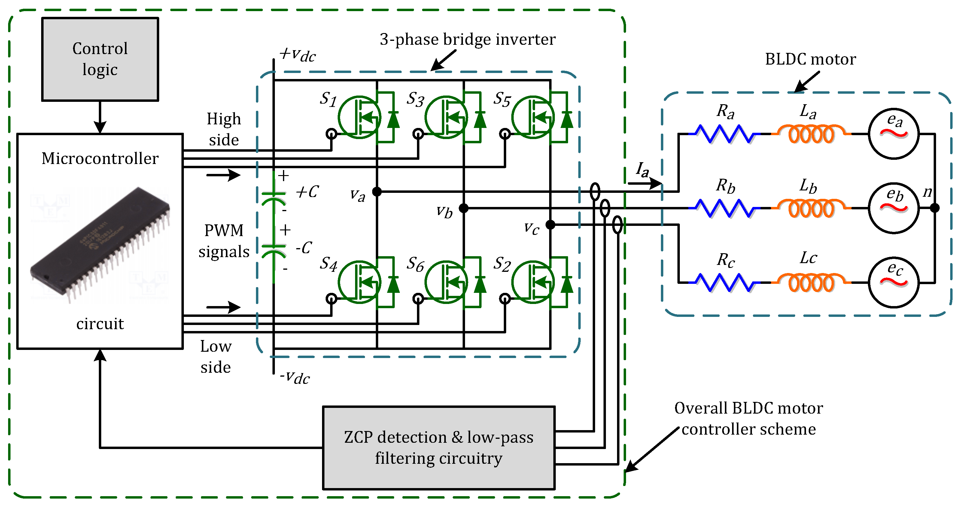
3. BLDC Motor Controller Theoretical Analysis and Design

The proposed topology of the BLDCM controller is shown in Figure 3 in block diagram form. It can be seen that it is governed by a modular “philosophy” rather than a single layout (the latter is mostly met in commercial products). The reason for this modular arrangement (as shown in later paragraphs) is primarily based on the easiness of the manufacturing process-as it is a prototype-and secondly on the easy maintenance, when this is a requirement (i.e., the repair of a module without affecting the rest of them. Based on this feature, the next paragraphs analyze each module separately.

3.1. Power Inverter Stage Module

This section focuses on the analysis and design of the control circuit, namely the inverter and the components of the hardware adopted. The three-phase power inverter use here is a full-bridge type in 120° electrical conduction mode. This operation is achieved by the simultaneous conduction of two phases while the third one is out. The stator rotating magnetic field is stepwise and not continuous. The inverter “moves” to the next stage of switching each time the rotor rotates by 60° electrical, thereby the stator magnetic field is changing. In a full rotation, there are six successive states corresponding to six magnetic states in the stator field. In each situation only two phases are in conduction mode, whereby a current flows into each winding during 120° electrical at each rotation of the stator field. In a general case, since the switching elements are not ideally switched “on” and “off”, some transition time (dead time) is required to avoid any short circuits in the branches (see Figure 1). However, for the topology of the inverter used here it is not necessary to introduce dead time because as shown in Figure 2a, the switching elements of the same sector (sector I-VI) are turned “on” by a 60° electrical difference.

3.1.1. Selection of MOSFETs

The semiconductor switching elements selection along with the corresponding heat-sinks is of primary importance in order to maximize the overall efficiency. These choices depend on the application. The most critical factors that influence the final choice are summarized below:
  • The voltage drop during the conduction and their conduction resistance determine the conduction losses of the element.
  • Switching times (on, off and transition times) determine the switching losses and set the switching frequency limits.
  • Current and voltage values determine the power required to be handled by the switching elements.
  • The cooling requirements, that is, the temperature coefficient of the conduction resistance of the element.
  • Cost is also an important factor when selecting items.
The following four types of switching elements are used in high power applications: thyristors, GTOs, IGBT and MOSFETs. Each one has a number of advantages and disadvantages that make it suitable for a particular application. The inverter manufactured in the context of this paper, operates at a fairly high frequency of 10 kHz–20 kHz (although 5 kHz–8 kHz could be sufficient), and can power a motor with nominal voltage equal to 24 V at 22 A on average (i.e., ~0.5 kW). This implies that the use of a thyristor and a GTO thyristor is rejected for the present application because they cannot operate at such switching frequency levels. In addition, IGBTs can operate at high frequencies and controlled voltage on their gate, but the rated operating voltage of the circuit is too small to allow the use of IGBTs. Thus, for the specific application, the MOSFET elements were selected. The use of AUIRF3205Z (from International Rectifier, El Segundo, CA, USA) was chosen based on the calculations shown below with emphasis given to lowest possible switching losses [30,31]. Its main characteristics are shown in Table 1. These features combined make this design an extremely efficient and reliable device for automotive applications as well as a wide range of other applications. It should be noted however, that for the sake of safety of the overall controller, i.e., in the event of over-voltages or high currents that may be caused by transient situations, many values are beyond the actual requirements of the application.
MOSFETs, as is well known, have a parallel “free-wheeling” (or else “fly-back”) diode embedded that allows the handling of reverse currents from the load to ground. The characteristics of the selected MOSFET diode are sufficient for the application requirements. The diode has a maximum reversal recovery time of 42 ns and a maximum forward voltage drop equal to VSD = 1.3 V.
The authors propose the addition of an extra diode between the gate and the source (G-S) of each semiconductor. A 18 V zener diode for MOSFET protection was employed here in case of an over-current fault. For example, if for any reason, the voltage between the gate and the source becomes greater than the maximum allowable, the diode will be forward biased and the voltage will remain constant at 18V preventing damage to the element.
Finally, the turn-“on” and turn-“off” speed of each MOSFET can be controlled by the value of the resistance connected in series to its gate, while regulating at the same time and the corresponding current. In order to determine this resistance it is necessary to take into account the gate-to-drain charge (Qgd), the gate-to-source charge (Qgs), the total gate charge (QG), the gate threshold voltage (VGSth), the voltage applied to the MOSFET gate (VDD) and the driver internal resistance (RDRV(on)). The required values are available from the manufacturer’s datasheet. Then, the gate resistance can be calculated by [32]:
R G = R t o t a l R D R V ( o n ) where   R t o t a l = V D D V g s ( t h ) I g ( a v g ) , I g ( a v g ) = Q g s + Q g d t s w and   R D R V ( o n ) = V D D I s o u r c e ,   I s o u r c e 1.5 Q G t s w , o n
For our case, Equation (9), gives a gate resistance of 38.5 Ω, thus a 39 Ω value was selected (R1, R2, and R3 in Figure 4). Figure 4 shows the analytical schematic diagram of the inverter. The aforementioned MOSFETs, zener diodes and gate resistances are shown clearly. The connectors shown lead to corresponding point of the rest schematics which will be shown in next paragraphs.

3.1.2. Cooling Considerations and Heatsink Calculations

The high switching frequency of the MOSFETs and the high current flowing through them, result in both conduction losses and switching losses. This, in turn, results in an increase in their temperature which-if not reduced-may lead to their destruction. Therefore, the temperature management of the semiconductor components is critical for the correct design of the system and the semiconductor longevity.
Heat dissipation is done by the use of appropriate heat sinks, which release the heat generated to the environment. Heat sinks consist of heat-conductive metal plates, which have many folds (fins) that maximize their surface area, thus transferring large amounts of heat to the environment. In order to reduce the thermal resistance between the semiconductor elements and the heat sinks, a thermally conductive but electrically insulating paste is inserted between the switch and the heat sink, which isolates the heat sink from the power circuit.
Total losses (Q) are the sum of conduction losses (Qc), switching losses (Qsw) and leakage losses (QL). The latter are quite small and are not taken into account. Conduction and switching losses are due to the operation of the semiconductor switches and the free-wheel diodes. The corresponding calculations proposed here are based on [30]. Thus we have:
Total   losses : Q = Q c + Q s w
Conduction   losses : Q c = Q c M O S + Q c D i o d e
where:
Q c M O S = R D S ( o n ) I D r m s 2 Q c D i o d e = R D I F r m s 2 I D r m s 2 = D I o 2 I F r m s 2 = ( 1 D ) I o 2 R D = Δ V S D Δ I S D
It is to be noted that in Equation (11), ΔVSD is the source-to-drain diode forward voltage and ISD is the reverse drain current between the ambient and operating temperature. Moreover, D is the duty cycle (assumed as 50%) and the RDS(on) value have to be considered at 100 °C. Continuing we have:
Switching   losses : Q s w = Q s w _ o n M O S + Q s w _ o f f M O S + Q s w _ o n D i o d e
where:
Q s w _ o n M O S = f s w ( U D D I D t r + t f 2 + Q r r U D D ) Q s w _ o f f M O S = f s w ( U D D I D t r + t f 2 )
where tr and tf are the rise and fall time respectively (in ns), Qrr is the reverse recovery charge (in nC) and fsw the operating switching frequency. Finally the thermal resistance (higher limit) value can be calculated by:
R s a m b = T j T a m b Q R j c R c s
where Tj, Tamb, Rjc and Rcs are the operating junction temperature, the ambient temperature, the junction to case thermal resistance and the case-to-sink thermal resistance respectively. Substituting the values found in the MOSFET datasheet to the above equations, the total losses found was Q = 7.23 W (which was the lowest compared to the ones found for six other candidate MOSFET examined) and the thermal resistance of the required heat sink found to be Rs-amb = 8.28 °C/W. Therefore, a heat sink with a resistance value lower than that must be selected. The heat sink selected here exhibits a thermal resistance of 6.5 °C/W, which is sufficient enough for continuous operation.

3.1.3. DC Bus Capacitor (Inverter Input)

Electrolytic capacitors should be used at the input of the three-phase inverter to act as filters to cutting off any over-currents during the opening/closing of the switching elements. The following relationship is used [33,34]:
C = V b u s 32 Δ V L f S W 2
For a dc bus voltage Vbus = 24 V, a lowest phase inductance of L = 20 μΗ, a minimum switching frequency fsw = 10 kHz and an acceptable voltage ripple (ΔV) as of 5%, Equation (15) gives C = 312.5 μF. Thus, a 470 μF/35 V capacitor was selected for the prototype.

3.2. Driver Stage Module

Full control of the three-phase inverter requires a control circuit, which generates the signals necessary to provide appropriate pulses to the MOSFETs. The control signals are generated by the microcontroller and follow a “route” as shown in Figure 5a. Initially, the signals are directed to a hex inverter chip which consists of 6 NOT gates and inverses them. The inverted pulses are driven then to opto-couplers which invert them again and at the same time provides galvanic isolation between the microcontroller and the power stage. Finally, the signals are fed to appropriate MOSFET driver chips which amplify them again and produce the final MOSFET driving pulse sequences.

3.2.1. Pulse Amplification and Galvanic Isolation

The microcontroller output signals are either 0 V or 5 V voltage pulses, however, to be able to drive the MOSFETs they must also be accompanied by a sufficient current. However, the output current of any microcontroller is not sufficient and for this reason, the output signals must be amplified before any processing and hence the need of a hex inverter chip. The chip selected here to amplify and inverse the signals coming out of the microcontroller is the SN74LS06 (Texas Instruments, Dallas, TX, USA) which consists of six NOT gates and is powered by 5V. Afterwards, the inversed and amplified pulses signals, are directed to an opto-coupler which achieves galvanic isolation between the control circuit and the power circuit. To achieve this isolation between the two circuits, there is a light-emitting diode at the inlet of the opto-coupler, which emits light when a voltage is detected. At its exit there is an open collector photo-transistor, with an isolation gap between them. From this gap no current can pass but light pulses, resulting in the separation of the Earth potentials of the two circuits and the protection of the control circuit from leakage currents. The opto-coupler used in this application is the HCPL2631 (Fairchild Semiconductors, San Jose, CA, USA) which fully covers the application requirements. It is powered by a 5 V voltage and outputs an inverted signal that now has the form it had when exited the microcontroller but is now amplified.

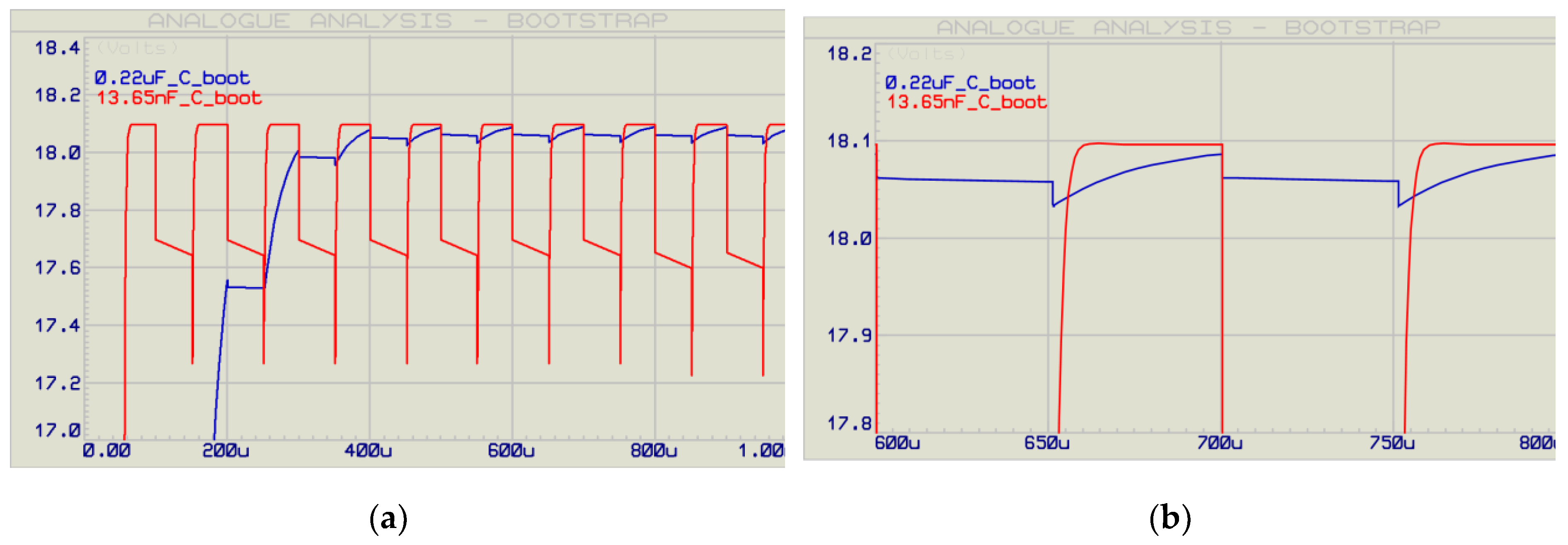
3.2.2. MOSFET Gate Driving and Bootstrap Circuit

This is the second part of the driver stage module (right half of Figure 5a). An appropriate chip should be selected here also which will be responsible to boost the pulses to the desired level of power to ensure that the MOSFETs are properly driven.
The IR2113 (International Rectifier) is one of the most robust, reliable as well as cheap choices, which can operate at high voltage and operating frequency and it exhibits two independent (high and low) output channels. Moreover, the latter cannot be activated simultaneously (which is desirable) as the chip has been designed for bootstrap mode operation (Figure 5b). The only disadvantage is that it needs two different supply voltages, 5 V (between Vcc and Vss) and another one in the range 10 V to 20 V (between Vcc and Com). In our application, a 15 V voltage was utilized. Thus, the incoming 5 V control signals are fed to the inputs HIN and LIN and the MOSFET gate signals are coming out from the outputs HO and LO at a 15 V level. The source pin of the low-side MOSFETs is permanently connected to ground, so that whenever a pulse comes to the LIN input, the LO output is connected to the 15 V supply. In contrast, the bootstrap methodology described in detail below is used to power the upper-side MOSFETs. Specifically, when the low-side MOSFET is in conduction mode, the VS of the upper one acquires the earth potential. The bootstrap capacitor (CBOOT) is then charged through the bootstrap diode (DBOOT) from the 15 V supply. When the lower MOSFET stops conducting and the upper one starts conducting, then the bootstrap capacitor discharges through upper MOSFET’s gate, so the latter can go off. The bootstrap diode in this case prevents the discharge current from flowing back to the VCC source. The bootstrap connection has the advantage of being simple and economical but it also has some limitations. The conduction start time and the duty cycle are limited by the charging requirements of the bootstrap capacitor. The major disadvantage of this method however, is that the negative voltage that occurs at the source of the MOSFET during turn off state, results in the load current being sharply directed to the free wheel diode of the lower side MOSFET. Negative voltage can be a problem for the output of the gate driver because it directly affects the VS terminal of the driver. Another problem arising from this negative voltage is the possibility of overvoltage at the bootstrap capacitor [32]. The bootstrap diode must have a slight voltage drop when conducting and a short reverse recovery time to minimize the load returning from the capacitor to the power supply. For this reason an ultra-fast recovery diode must be used. Therefore, the UF4007 diode was selected which was placed very close to the bootstrap capacitor. Moreover, the capacitor shall be of sufficient capacity to supply the necessary current to ignite the upper MOSFET and maintain its voltage during conduction. For this purpose, a 0.22 µF/35 V tantalum capacitor was used. Tantalum capacitors have been chosen because they have high capacitance, low internal resistance (ESR) and minimal leakage current compared to electrolytic, polypropylene or ceramic counterparts. The calculation for the capacity of the bootstrap capacitor is given below. Firstly, it is necessary to calculate the minimum ΔVBS voltage that must be maintained by the capacitor when the upper MOSFET is conducting, i.e.,:
Δ V B S V C C V f V G S min
where Vcc is the supply voltage of the IR2113 (15 V), Vf is the diode voltage drop (1.7 V) and VGSmin is the minimum voltage needed for maintaining the conduction of the MOSFET (4 V). Afterwards, the total charge stored in the capacitor should be calculated:
Q t o t = Q g a t e + ( I L K c a p + I L K G S + I Q B S + I L K + I L K D i o d e ) t o n + Q L S
where ILKcap is the bootstrap capacitor leakage current, ILKGS is the MOSFET gate-source leakage current, IQBS is the bootstrap circuit quiescent current, ILK is the bootstrap circuit leakage current, ILKDiode is the bootstrap diode leakage current, ton is the MOSFET conduction delay time and QLS is the charge required by the internal level shifter (which is set to 3 nC for all HV gate drivers).
Finally, Equation (18) gives the capacitor value which in our case resulted in 13.65 nF. For this application, tantalum capacitors with a capacity of 0.22 μF, i.e., 16 times greater than the calculated value, were selected to extinguish the possibility of rapid capacitor discharge during MOSFET conduction:
C B O O T = Q t o t Δ V B S
Specifically, according to [35,36], the bootstrap capacitor is the most important component because it provides a low impedance path to source the high peak currents to charge the high-side switch. As a general rule of thumb, this bootstrap capacitor should be sized to have enough energy to drive the gate of the high-side MOSFET without being depleted by more than 10%. This bootstrap cap should be at least 10 times greater than the gate capacitance of the high-side FET. The reason for that is to allow for capacitance shift from DC bias and temperature, and also skipped cycles that occur during load transients. Here, we followed a more accurate approach on the total charge calculation (Equation (17)) taking into account analytically all the relevant components leakage currents and thus the "16x" factor is justified.
In order to demonstrate the charging/discharging waveforms of the calculated and the selected values bootstrap capacitor, Figure 5a was implemented into a suitable transient analysis simulation software (Proteus v.8.9 by Labcenter Electronics©, Grassington, North Yorkshire, UK). In Figure 6, the relevant results are shown, from where it can be observed that the 0.22 μF capacitor used presents a much more "stable" operating pattern being depleted only by 0.2% compared to the 13.65 nF one which—when discharging—is being depleted by approximately 5% in every cycle.

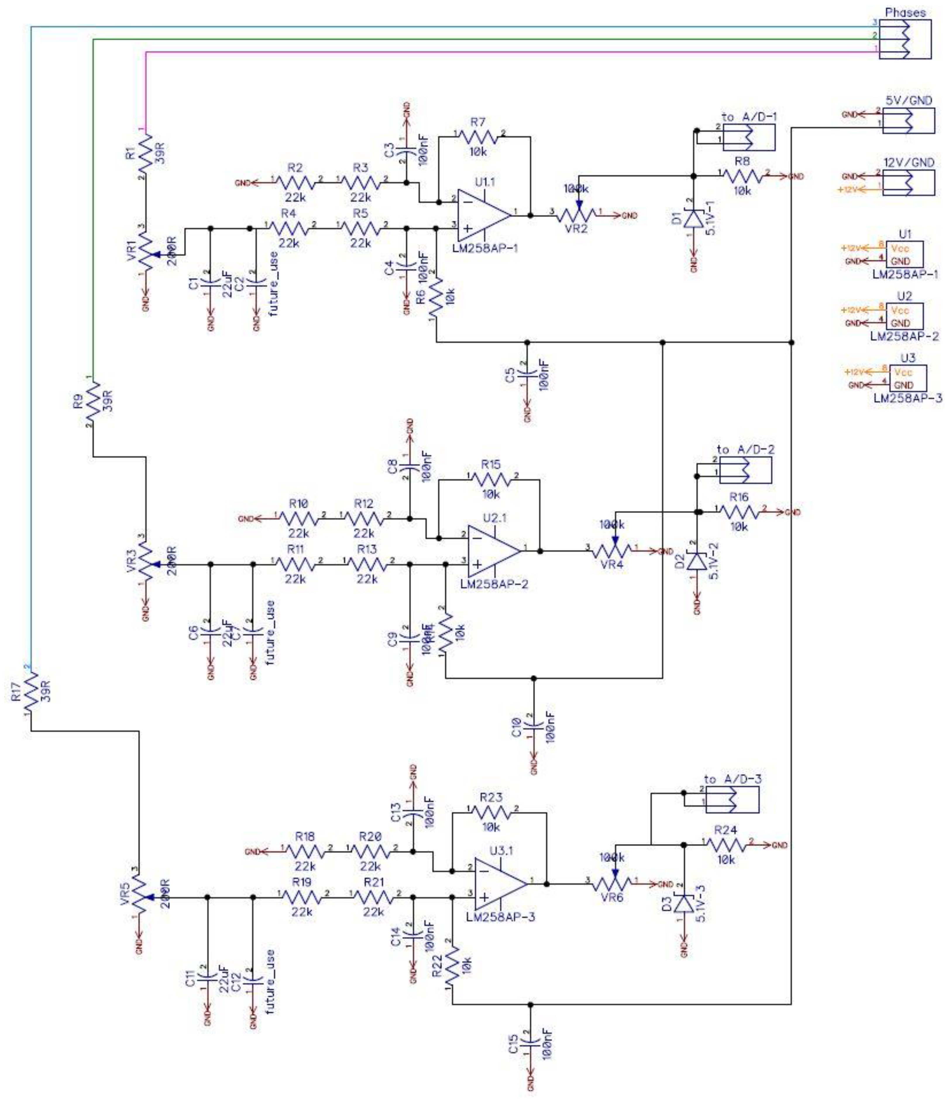
3.3. Back-EMF Measurement & Low Pass Filtering Modules

3.3.1. Back-EMF Measurement

Since the operating voltage of the microcontroller is 5 V it is necessary to condition (i.e., transform to appropriate voltage levels) the back-EMF voltages acquired from the BLDCM terminals. There are several methods to do this. The most cost effective and yet effective way is to use an operational amplifier (op-amp) in differential mode. The circuit shown in Figure 7 was implemented for that purpose (three identical circuits one for each phase). The goal of the circuit is to "receive" an incoming voltage between −24 V to 24 V and to convert it to [0, 5] level.
The LM258-N integrated circuit from Texas Instruments was used to implement the circuit which requires a positive power supply of up to 32 V (pin 8). In this application it was supplied with 12 V DC voltage from the power supply module. The differential amplifier’s positive input is connected to the terminal of each phase of the motor and the negative input is grounded. According to the manufacturer’s datasheet, the current at the input should not exceed 50 mA. For this reason a number of resistors at the inputs of the operator were used to limit the input current. In this application the maximum voltage can reach 22 V, so two 22 kΩ resistors were selected to be placed in series. Continuing, the gain of the op-amp can be determined. By selecting a 10 kΩ as a feedback resistance, the gain is calculated as 0.227 and thus the output voltage of the op-amp is Vout = gainxVin = 0.227x ± 22 V = ±5 V. A 5 V voltage is added to the op-amp output voltage giving 0–10 V and finally a voltage divider (using a 10 kΩ resistor along with a variable potentiometer for calibration) is applied to convert the range to 0–5 V.
To reduce the noise in the power supply lines, 100 nF capacitors were used at the power terminals of each integrated circuit. With the use of these capacitors, high-frequency currents flow through them and do not enter the power lines. Also at the output of each op-amp a 5.1 V zener diode was connected for protecting the microcontroller if the voltage goes above the permissible limits.

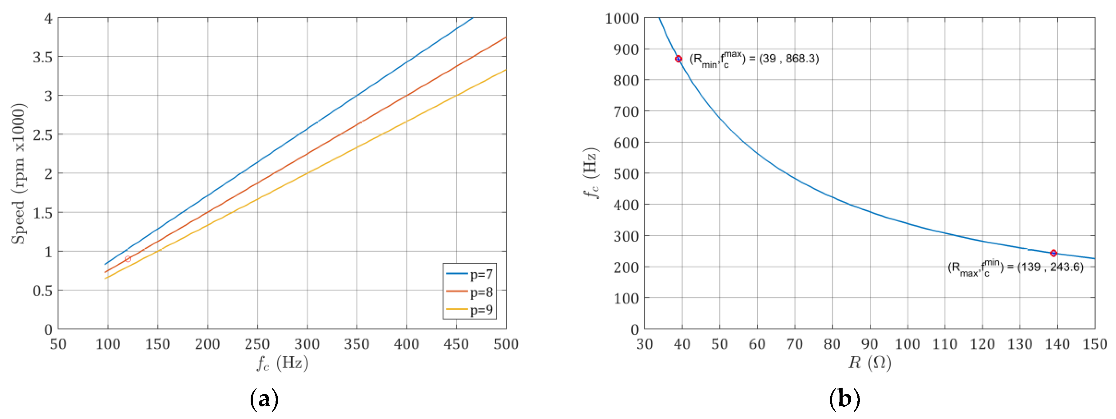
3.3.2. Low Pass Filter

In such BLDCM controller systems, high frequency voltage spikes and/or electromagnetic interference noise may be generated by the motor during operation and also from the switching elements (due to their high operating frequencies). Thus, in order to eliminate voltage high frequency components, it is necessary to design and implement a simple low-pass filter, one for each motor phase. This is crucial for the reliable ZCP detection because the noise would lead to inaccurate zeros “reading” and as a result incorrect phase switching would occur. The filter should be placed between the motor terminals (its input) and the op-amp described in the previous paragraph (as its output) as shown in the left part of Figure 7.
The following example is provided for easier understanding of the filter components (Rf, Cf) selection. Let us suppose that the motor has eight pair of poles (p) and a rated speed (n) of 900 rpm. Thus, the motor’s voltage frequency at 900 rpm is 120 Hz (since n = 60f/p) as it can be seen in Figure 8a. If we want to eliminate the higher harmonics (3rd, 5th, etc.) then the cut-off frequency must be at least 360 Hz. By setting a capacitor value at Cf = 4.7 μF and applying the well-known formula, the resistance Rf of the filter must be approximately 94 Ω (which in practice can be realized by using a potentiometer). Correspondingly, the cut-off frequency can also be derived by means of a graph similar to Figure 8b:
f c = 1 2 π R f C f
For our application, the goal was to cut frequencies higher than 250 Hz. A constant value resistance of 39 Ω was used in series with a 100 Ω potentiometer, and also a polyester type capacitor (MKT) at 4.7 µF/100 V, which is suitable for the desired frequency range. Using the potentiometer it is possible to vary the Rf in a range 39 Ω to 139 Ω. This allows the cut-off frequency to range from 243.6 Hz to 868.3 Hz respectively (shown in Figure 8b). This adopted technique allows for operating the controller in a wide range of filter responses and make the application more generic targeting to different pole pairs motors.

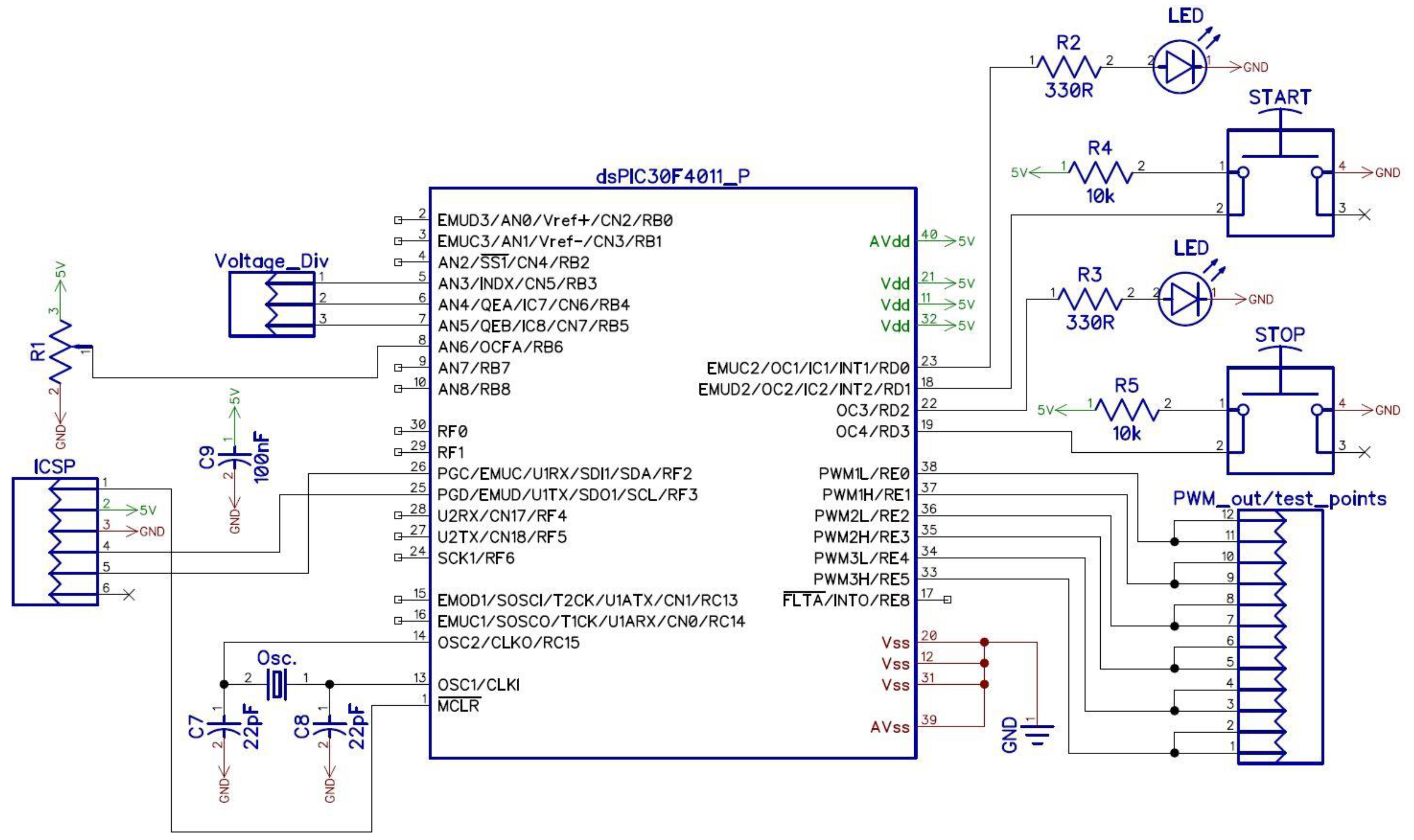
3.4. Microcontroller Module

Nowadays, the family of microcontrollers provided by the manufacturers (e.g., Microchip, Chandler, AZ, USA) is so large that their selection towards an application is rather a “personal affair” than a technical prescript. However, there are quite a few general guidelines which may be followed as those listed below. Based on these, the Microchip© dsPIC30F4011 μC was selected. The main reasons are:
  • It is well suited for control applications of motors since it provides three independent PWM output pairs allowing the control of three-phase and single-phase inverters.
  • It can process and execute complex digital signal calculations very quickly as required for BLDCM control.
  • It is manufactured in DIP package and therefore it is suitable for prototyping and breadboard use.
  • It can operate in a wide range of power supply (2.5–5.5 V).
  • It can withstand wrong voltage levels that by mistake may be applied to its terminals without being damaged.
  • It can be found in the market easily and is generally cheap.
  • Its development program (MPLAB and compiler) is available free of charge from the manufacturer.
  • It is equipped with enough I/O ports for interconnecting peripherals.
  • It has nine analogue input channels available, of 10-bit resolution.
The basic operating principles are common for all 30F-family chips so the software code developed can be easily transferred (software portability) if other model is later needed to be employed. The schematic diagram of the μC module developed is shown in Figure 9. A 20 MHz oscillator was used. Two push buttons (start/stop) were also utilized for the controller’s operation.

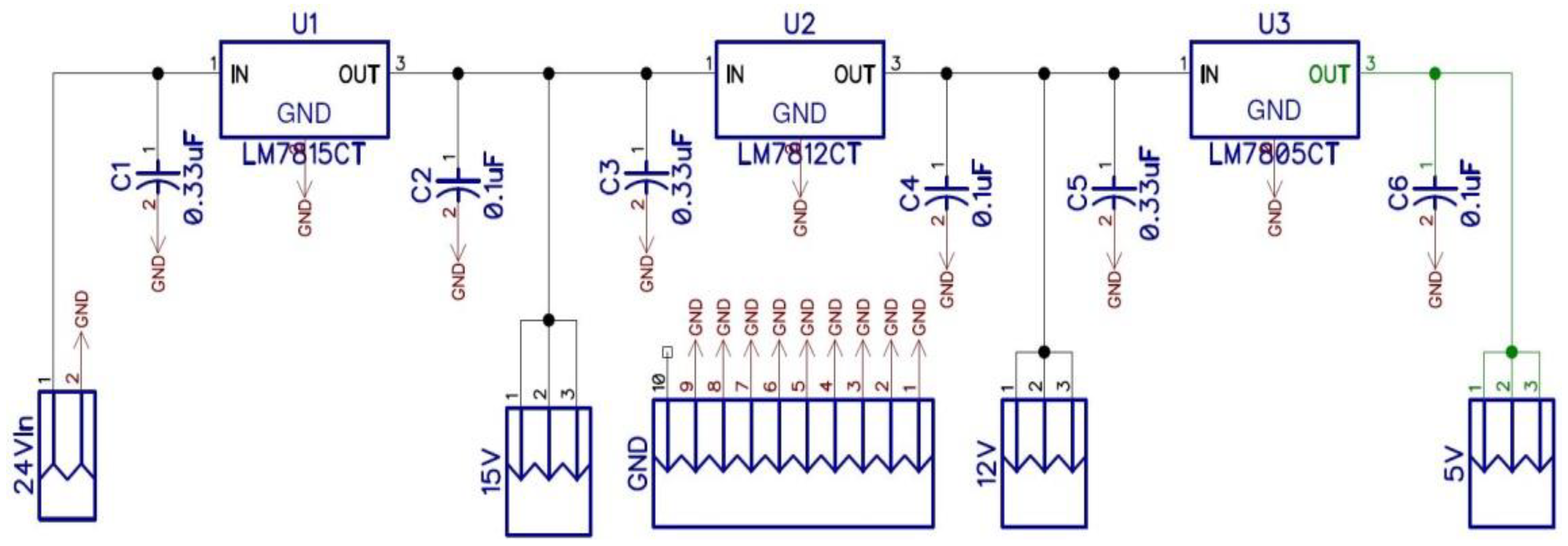
3.5. Power Supply Module

The overall controller requires different DC supply voltages for the different modules. Most of them require 5 V. However the gate drivers require both 5 V and 15 V and the integrated circuits for the motor terminal voltage conditioning to the microcontroller voltage level require 12 V. Since the developed controller is to be used in stand-alone application, the only power source will be a 22 V/5000 mAh, 6 cell, lithium polymer battery. Therefore, the battery voltage should be stepped down to 15 V, 12 V and 5 V, with the least power losses. Although three buck converters could be used, the cost would be high, so the solution was to use cheap voltage regulators. Specifically, Fairchild’s LM7805, LM7812, LM7815 regulators were used in cascade connection. Their maximum power output is 1 A, which is more than enough for the low-power modules. For each voltage level, the output of each regulator is driven to three terminal bus-bars whereas afterwards the other modules are fed through them. This power supply module is “hosted” at the same board with the microcontroller module. The schematic diagram of the power supply module is shown in Figure 10.

3.6. Supplementary Passive Components Used

Various supplementary passive elements are also proposed and used here to protect the rest of the components (mainly for the control and the power modules). With respect to Figure 4, Figure 5, Figure 7, Figure 9 and Figure 10, these are:
  • Pull-up resistors (330 Ω) were installed between the power supply of the hex-inverter and its outputs, in order to limit the input current to the capacitors below 20 mA and to enable the circuit to supply the input of the next connected element with the output of the hex inverter as long as the transistor of the latter is in cut-off mode. This is because the specific chip’s (SN74LS06) gates are operating through an embedded open-collector transistor.
  • Pull-down resistors (10 kΩ) were added between the inputs of the hex inverter and the ground. That is necessary, in case any of the terminals found unconnected for any reason, then its output would be in zero state, otherwise we may face unwanted MOSFET firing or simultaneous firing of MOSFETs of the same leg, which would lead to controller failure.
  • Between the outputs of the opto-couplers and the 5 V power supply, 330 Ω (pull-up) resistors were also installed to limit their embedded photo-transistor’s collector current and to enable the circuit to supply properly the next module stage.
  • In every module, in order to reduce noise in the power lines, ceramic capacitors of 100 nF were connected so that high frequency currents would flow through them and not the power lines.
  • In order to set the desired motor speed i.e., changing the PWM duty cycle, a 5 V/10 kΩ slider potentiometer was used.

4. Developed Control Strategy and Relevant Software

4.1. Control Philosophy

The overall circuit control strategy is essentially implemented in software source code by six routines in total. The first three of them are (a) the motor starting and the alignment of the rotor routine, (b) the open loop routine and (c) the closed loop routine, and actually correspond to the three possible BLDCM operating conditions. Another two important routines (implemented as interrupts) are also implemented, a routine that converts the signals from analog to digital (ADC interrupt) and a second one for a necessary precision timer (interrupt of microcontroller’s "Timer1"). Additionally, the control process initialization was done by coding a necessary initialization routine. The code was designed in C language and the Microchip© XC16 compiler was used to compile it. It was of great help to the software development, the fact that the dsPIC30F4011 is specifically engineered for motor control applications, and therefore offers various features to the developer, including the fully customizable PWM pulse generation. The software implementation is represented by the basic flowchart which is depicted in Figure 11a.

4.2. Main Routine

This is the main routine of the program. It initializes the variables used and calls the initialization routines of the microcontroller units (PWM, A/D, Timer). In addition, it controls the operation of the start/stop switch by changing the status variable and invokes the corresponding routines. The flowchart of this routine is shown in Figure 11a and the corresponding code is given in Appendix B, under the name “Routine A”.

4.3. Rotor Alignment Routine

This routine is used to start and align the BLDCM rotor. The technique used here is easy and described next. Initially, the duty cycle is set to 50% and the 3rd sector is activated (S3, S2), according to Figure 1 and Table 2. The PWM signal is applied for a period of time (1–2 s is more than enough) to ensure the rotor alignment and then the 5th sector is activated (S5, S4) for another period of time which assures the starting of the rotor rotation. The flowchart of this routine is shown in Figure 11b and the corresponding code is given in Appendix B, under the name “Routine B”.

4.4. Control Loops Routines

As mentioned in Section 4.1, two loop control modes were implemented for this application: a manual open loop control mode and a closed loop control mode which is governed by a simple PI controller. The corresponding software developed is presented next.

4.4.1. Open Loop

Open-loop starting is a practical control procedure to run the BLDC motor without position sensors that is accomplished by providing a rotating stator field with a certain frequency profile [16], either in manual or automatic mode. In our case, the latter was chosen where the PWM duty cycle ratio and therefore the motor speed varies manually according to the value of the control potentiometer. Sector VI commutating sequence is initiated for a time period set by dsPIC’s “Timer1” and varies according to the desired speed each time. If the motor speed exceeds 100rpm, the process goes on the closed loop mode. The flowchart of this routine is shown in Figure 12a and the corresponding code is given in Appendix B, under the name “Routine C”.

4.4.2. Closed Loop

In terms of stable operation, this routine handles programmatically the two interrupt service routines (ISR) as well as host the PI control operation. In terms of controller stable performance, it is very crucial and can be fully parameterized. Initially, the actual motor speed is compared to the reference speed and an error is generated which is used in the PI controller to generate the new PWM duty cycle value. For safety reasons, this value is limited between 0.2 and 1.0, and then the motor windings are excited for a certain period of time. The duration interval depends on the detection of zeros points in the line voltages as will be explained below in the A/D ISR operation. Finally, sampling of phases A, B, C. are performed and the cycle continues. If the speed drops below a threshold value (e.g., 100 rpm) due to a loading condition, the program flow jumps to open loop operation. The flowchart of this routine is shown in Figure 12b and the corresponding code is given in Appendix B, under the name “Routine D”.

4.5. Interrupt Services Routines

This class of routines serves two program interrupts, including the ADC ISR and the Timer1 ISR. Specifically, the ADC routine is used for sampling the line voltage signals and searching for zero crossing points. When finding a ZCP the commutation sequence is performed according to Table 2. In particular, if a ZCP is found for phase A, then Timer2 is also activated to calculate the actual motor speed. On the other hand, the Timer1 routine is used to calculate the phase transition time of the motor during its alignment operation and when operating in open loop. The flowchart of ADC ISR is shown in Figure 13a and the corresponding code is given in Appendix A, under the name “Routine F”. The flowchart of Timer1 ISR is shown in Figure 13b and the corresponding code is given in Appendix A, under the name “Routine E”.

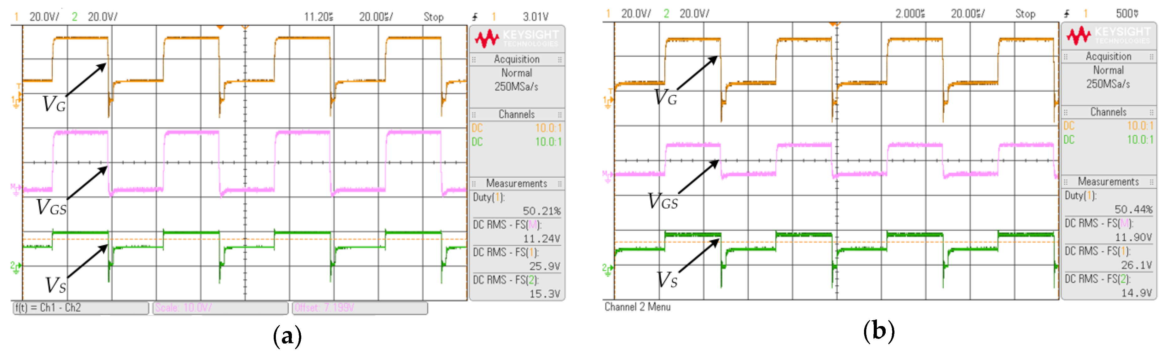
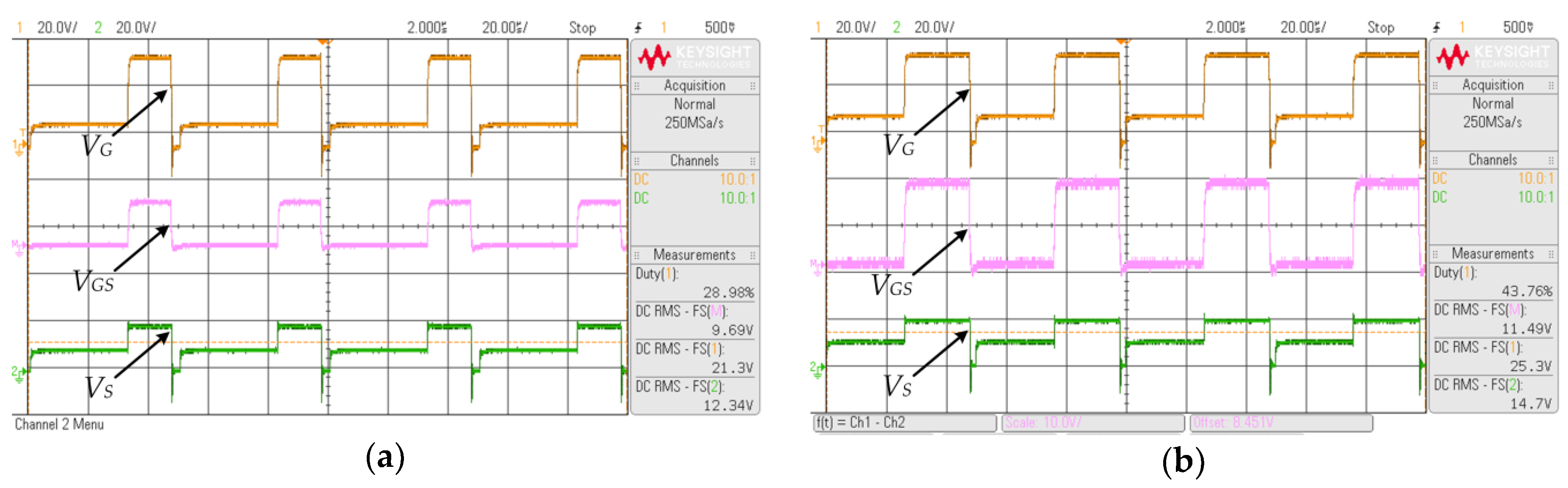
5. Experimental Prototype’s Indicative Results

The presented controller module schematics were first developed with the aid of Novarm© Diptrace software (Kedrina, Dniepropetrovsk, Ukraine), and then the corresponding printed circuit boards (PCBs) were designed manually in order for the modules to present the required connection alignment in the final form. Special care was taken in specific trace routes where large currents may flow (from the power source through MOSFETs and to motor). Afterwards the PCBs designs were transferred onto photo resistive copper clad boards which were drilled and used for assembling the components. Single sided copper boards were selected for simplicity in manufacturing. The assembled modules and the connection between them, composed an experimental test bed where test runs were performed. A view of the test bed is depicted in Figure A2a in Appendix A. The final prototype is depicted in the same Figure A2b in the same Appendix. A small hobby BLDCM like those used in remote control models (i.e., airplanes, drones) where utilized as a test motor.
Initially, some experiments were carried out regarding the generated PWM pulses. Figure 14 actually verifies the correct PWM signals feeding, based on the methodology of Section 3.2 for the circuit shown in Figure 5a. Specifically, for a 20 kHz switching frequency, the pulses generated by the microcontroller’s output are fed to the SN74LS06 which inverts them and, in turn, feed the HCPL2631 opto-coupler. As can be seen in Figure 14a the pulses from the output of HCPL2630 are identical to the pulses originally generated by the microcontroller. Continuing, Figure 14b verifies the correct operation of the IR2113 MOSFET driver. It can be seen that compared to the pulse amplitude at the input of SN74LS06 (3.16 V), the output pulse from the IR2113 has been appropriately amplified (10.48 V) in order to drive the MOSFETs gate.
The rest of the experimental validation, concerns the proper functioning of the MOSFETs, by examining the gate-to-source voltage (VGS). Four operation scenarios were chosen for which indicative measurements in open-loop control mode were conducted and shown next. These scenarios are: (a) Case 1: operation with constant duty cycle and constant speed, (b) Case 2: operation with constant duty cycle and variable speed, (c) Case 3: operation with variable duty cycle and constant speed and (d) Case 4: operation with variable duty cycle and variable speed. For all cases the gate-to-source voltage of the inverter’s upper leg MOSFET was obtained by differential measurement. The differential measurement was made between the gate and the ground (orange waveform) and the source and the ground (green waveform). For each case, the motor is initially aligned and, just after, enters into an open loop mode where it can be driven (through user command) up to a speed of 100 rpm. When this speed is exceeded, a transition occurs to closed loop mode. Because of space limitations, indicative results are shown in this paper. The essential element of these controller types is the proper operation of the bootstrap circuit which drives the upper part of the inverter’s bridge, and therefore the MOSFET voltages are examined. Figure 15a refers to Case 1 and depicts the VGS voltage (along with the gate voltage, VG and the source voltage, VS) under 140 rpm and a duty cycle equal to 50%. For the same duty cycle, Figure 15b refers to Case 2 and shows the VGS voltage for approximately the same speed. Figure 16a corresponds to Case 3 and for a duty cycle of approximately 30% and speed close to 100 rpm, the same voltage is shown. Figure 16b depicts the VGS voltage for approximately 89 rpm and a duty cycle of 43.8%. In all Cases, it can be deduced from the waveforms that actually the bootstrap capacitor charges/discharges in a smooth way. It can also be deduced that the attained switching frequency has a magnitude of more than 25 kHz (<40 μs period).
Finally, a simple cost comparison with commercial BLDCM sensorless controllers is demonstrated in Table 3 where it is clearly shown the cost superiority of the controller developed here and for higher motor ratings. However, it should be noted, that this Table is just for relative information and not for actual comparison, since (a) the cost of the implemented controller represents only material costs and (b) we have to acknowledge that the commercial controllers present many features not examined in this study.

6. Conclusions

The purpose of this paper was to present a descriptive as well as informative straightforward practical implementation method of a low cost BLDCM sensorless controller. Having simplicity and low cost as a priority, several issues regarding the hardware components selection were discussed and commented. A modular-based design was adopted for comprehensibility and easiness in manufacturing process. Based on a suitable-for digital signal processing-microcontroller, the PWM pulses generation and their driving up to the power inverter MOSFETs was discussed in detail and simple techniques were proposed. A bootstrap circuit was implemented as the main driving hardware. Regarding the power inverter, analytical calculations were shown for the proper selection and cooling of the switching elements. For the control strategy, a variant of the well-known zero crossing point detection method was utilized, based on the back-EMF differences signals and a suitable conditioning circuit was also presented. Detailed schematics of the proposed architecture clarified the overall controller scheme. Moreover, the aforementioned control strategy adopted was analyzed thoroughly, based on the simplicity and portability. Relative software source code developed was also given as a reference. Finally, indicative experimental results from the controller operation revealed the reliable and proper functionality.
There are many points which future work efforts can target. One includes the careful replacement of the majority of the components with surface mounted devices (SMD) towards lower size and weight. Redesigning the modules structure “from scratch” is another thought, towards maintenance flexibility (easy replacement or service). Another, more technical issue, would be the addition of transition voltage suppress diodes (TVS) at the inverter stage input, which would suppress major voltage peaks observed in oscilloscope during commutation sequence transitions. In software level, there are also some potential improvements as a future work framework. For example, it would be useful during the start-up and alignment process to take into account some motor quantities (by storing them into a static memory), such as its idle torque, so that the start-up time would be adjusted appropriately each time a different motor is used (i.e., specific motor profile operation). It would be also useful to develop a graphical interface (either stand-alone or through USB connection to a PC) that would inform the user about e.g., motor speed, phase currents, line voltages, etc.). Last but not least, optimal tuning of the PI controller parameters for enhanced operation in closed loop would be of interest also. Moreover, the investigation of using two different sets of parameters, one for the open loop mode and the other for the closed loop mode (which would be changing automatically), would have been of great interest too.

Author Contributions

All authors are involved developing the concept, simulation and experimental validation and to make the article error free technical outcome for the set investigation work.

Funding

This research received no external funding.

Conflicts of Interest

The authors declare no conflict of interest.

Appendix A. Prototype Modules Photos and Experimental Set-Up Description

Figure A1. Developed BLDCM controller PCBs: (a) 3-phase power inverter circuit module; (b) PCB hosting the inverter driving module (c) back-EMF detection circuit module along with the low-pass filters; (d) power supply and microcontroller module.
Electronics 08 01456 g0a1
Figure A2. The presented here BLDCM controller (a) the experimental test bed; (b) final assembled view.
Electronics 08 01456 g0a2

Appendix B. C Language Software Code Developed and Loaded to dsPIC30F4011 Microcontroller

Electronics 08 01456 i001
Electronics 08 01456 i002

References

  1. Krishnan, A.R. Electric Motor Drives: Modeling, Analysis, and Control, 1st ed.; Prentice Hall Inc.: New Jersey, NJ, USA, 2001. [Google Scholar]
  2. Hanselman, D.C. Brushless Permanent-Magnet Motor Design, 2nd ed.; Magna Physics Publishing: Ohio, OH, USA, 2003. [Google Scholar]
  3. Gieras, J.F. Permanent Magnet Motor Technology, Design and Applications, 3rd ed.; CRC Press: Boca Raton, FL, USA, 2009. [Google Scholar]
  4. Gupta, N.; Mohan, M.; Pandey, A.K. A review: Sensorless control of brushless DC motor. Int. J. Eng. Res. Technol. 2012, 1, 1–6. [Google Scholar]
  5. Lee, W.J.; Sul, S.K. A new starting method of BLDC motors without position sensor. IEEE Trans. Ind. Appl. 2006, 42, 1532–1538. [Google Scholar] [CrossRef]
  6. Vasudevan, K.; Damodharan, P. Sensorless brushless DC motor drive based on the zero-crossing detection of back electromotive force (EMF) from the line voltage difference. IEEE Trans. Energy Convers. 2010, 25, 661–668. [Google Scholar]
  7. Gao, Y.; Liu, Y. Research of sensorless controller of BLDC motor. In Proceedings of the IEEE 10th International Conference on Industrial Informatics (INDIN), Beijing, China, 25–27 July 2012. [Google Scholar]
  8. Shao, J.; Nolan, D.; Hopkins, T. Improved direct back EMF detection for sensorless brushless DC (BLDC) motor drives. In Proceedings of the 18th Annual IEEE Applied Power Electronics Conference and Exposition (APEC), Miami, FL, USA, 9–13 February 2003; Volume 1. [Google Scholar]
  9. Tong, C.; Wang, M.; Zhao, B.; Yin, Z.; Zheng, P. A novel sensorless control strategy for brushless direct current motor based on the estimation of line back electro-motive force. Energies 2017, 10, 1384. [Google Scholar] [CrossRef]
  10. Zhu, Z.Q.; Ede, J.D.; Howe, D. Design criteria for brushless dc motors for high-speed sensorless operation. Int. J. Appl. Electromagn. Mech. 2001, 15, 79–87. [Google Scholar] [CrossRef]
  11. Merin, J.; Vinu, T. Position sensorless control of BLDC motor based on back EMF difference estimation method. In Proceedings of the International Conference on Power and Energy Systems Conference: Towards Sustainable Energy (PESTSE), Bangalore, India, 13–15 March 2014. [Google Scholar]
  12. Chen, C.H.; Cheng, M.Y. A new cost effective sensorless commutation method for brushless DC motors without phase shift circuit and neutral voltage. IEEE Trans. Power Electron. 2007, 22, 644–653. [Google Scholar] [CrossRef]
  13. Niasar, A.H.; Moghbeli, H.; Kashani, E.B. A low-cost sensorless BLDC motor drive using one-cycle current control strategy. In Proceedings of the 22nd Iranian Conference on Electrical Engineering (ICEE), Tehran, Iran, 20–22 May 2014. [Google Scholar]
  14. Park, J.S.; Lee, K.-D.; Lee, S.G.; Kim, W.-H. Unbalanced ZCP compensation method for position sensorless BLDC Motor. IEEE Trans. Power Electron. 2018, 34, 3020–3024. [Google Scholar] [CrossRef]
  15. Chang, P.I.-T.; Lin, X.-Y.; Yu, I.-J. Sensorless BLDC motor sliding mode controller design for interference recovery. In Proceedings of the 6th International Conference on Control, Decision and Information Technologies (CoDIT), Paris, France, 23–26 April 2019. [Google Scholar]
  16. Krishnan, R.; Ghosh, R. Starting algorithm and performance of a PM DC brushless motor drive system with no position sensor. In Proceedings of the 20th IEEE Power Electronics Specialists Conference (PESC), Milwaukee, WI, USA, 26–29 June 1989; pp. 815–821. [Google Scholar]
  17. Zhou, X.; Chen, X.; Peng, C.; Zhou, Y. High performance non-salient sensorless BLDC motor control strategy from standstill to high speed. IEEE Trans. Ind.Inf. 2018, 14, 4365–4375. [Google Scholar] [CrossRef]
  18. Ziaeinejad, S.; Sangsefidi, Y.; Shoulaie, A. Analysis of commutation torque ripple of BLDC motors and a simple method for its reduction. In Proceedings of the 2011 International Conference on Electrical Engineering and Informatics (ICEEI), Bandung, Indonesia, 17–19 July 2011. [Google Scholar]
  19. Devendra, P.; Kalyan, P.; Mary, K.A.; Ch, S.B. Simulation approach for torque ripple minimization of BLDC motor using direct torque control. Int. J. Adv. Res. Electr. Electron. Instrum. Eng. 2013, 7, 3703–3710. [Google Scholar]
  20. Lu, H.; Zhang, L.; Qu, W. A new torque control method for torque ripple minimization of BLDC motors with un-ideal back EMF. IEEE Trans. Power Electr. 2008, 23, 750–758. [Google Scholar] [CrossRef]
  21. Chowdhury, D.; Chattopadhyay, M.; Roy, P. Modelling and simulation of cost effective sensorless drive for brushless DC motor. In Proceedings of the International Conference on Computational Intelligence: Modelling, Techniques and Applications (CIMTA), Kalyani, India, 27–28 September 2013; pp. 279–287. [Google Scholar]
  22. Kamalapathi, K.; Priyadarshi, N.; Padmanaban, S.; Holm-Nielsen, J.B.; Azam, F.; Umayal, C.; Ramachandaramurthy, V.K. A Hybrid Moth-Flame Fuzzy Logic Controller Based Integrated Cuk Converter Fed Brushless DC Motor for Power Factor Correction. Electronics 2018, 7, 288. [Google Scholar] [CrossRef]
  23. Jamshidi, J.; Tohidi, H. Sensorless control strategy for brushless DC motor drives based on sliding mode observer. Int. J. Comput. Sci. Netw. Secur. 2016, 16, 43–48. [Google Scholar]
  24. Sathyan, A.; Milivojevic, N.; Lee, Y.J.; Krishnamurthy, M.; Emadi, A. An FPGA-based novel digital PWM control scheme for BLDC motor drives. IEEE Trans. Ind. Electr. 2007, 56, 3040–3047. [Google Scholar] [CrossRef]
  25. Karnavas, Y.L.; Topalidis, A.S.; Drakaki, M. Development of a low cost brushless DC motor sensorless controller using dsPIC30F4011. In Proceedings of the 7th International Conference on Modern Circuits and Systems Technologies (MOCAST), Thessaloniki, Greece, 7–9 May 2018; pp. 1–4. [Google Scholar]
  26. Lee, B.K.; Kim, T.H.; Ehsani, M. On the feasibility of four-switch three-phase BLDC motor drives for low cost commercial applications: Topology and control. IEEE Trans. Power Electr. 2003, 18, 164–172. [Google Scholar]
  27. Gamazo-Real, J.C.; Vázquez-Sánchez, E.; Gómez-Gil, J. Position and speed control of brushless DC motors using sensorless techniques and application trends. Sensors 2010, 10, 6901–6947. [Google Scholar] [CrossRef]
  28. Damodharan, P.; Sandeep, R.; Vasudevan, K. Simple position sensorless starting method for brushless DC motor. IET Electr. Power Appl. 2008, 2, 49–55. [Google Scholar] [CrossRef]
  29. Astik, M.B.; Bhatt, P.; Bhalja, B.R. Analysis of sensorless control of brushless DC motor using unknown input observer with different gains. J. Electr. Eng. 2017, 68, 99–108. [Google Scholar] [CrossRef] [Green Version]
  30. Graovac, D.; Purschel, M.; Kiep, A. MOSFET power losses calculation using the datasheet parameters. Application Note, Infineon Technologies AG, ver 1.1, July 2006. Available online: http://application-notes.digchip.com/070/70-41484.pdf (accessed on 25 May 2019).
  31. Kahrimanovic, E. Power Loss and Optimized MOSFET Selection in BLDC Motor Inverter Designs; White paper; Infineon Technologies AG: Neubiberg, Germany, 2016; pp. 1–31. [Google Scholar]
  32. Fairchild Semiconductor Corporation. Design and application guide of bootstrap circuit for high-voltage gate-drive IC. Application Note, no. AN-6076, revision date 18 December 2014. Available online: https://www.onsemi.com/pub/Collateral/AN-6076.pdf (accessed on 25 May 2019).
  33. Salcone, Μ.; Bond, J. Selecting film bus link capacitors for high performance inverter applications. In Proceedings of the IEEE International Electric Machines and Drives Conference (IEMDC), Miami, FL, USA, 3–6 May 2009. [Google Scholar]
  34. Furst, F. Design of a 48 V three-phase inverter for automotive applications. Master’s Thesis, Department of Energy and Environment, Chalmers University of Technology, Gothenburg, Sweden, 2015. [Google Scholar]
  35. Zheng, S. TPA31xxDx Bootstrap Circuit. Application Report No. SLOA259, Texas Instruments, Dallas, Texas, November 2017. Available online: https://www.ti.com/ (accessed on 25 May 2019).
  36. Diallo, M. Bootstrap Circuitry Selection for Half-bridge Configurations. Application Report No. SLUA887. High Power Drivers Group, Texas Instruments: Dallas, TX, USA, August 2018. Available online: https://www.ti.com/lit/an/slua887/slua887.pdf (accessed on 25 May 2019).
Figure 1. Simplified topology illustration of a sensorless BLDCM control scheme utilizing ZCP.
Electronics 08 01456 g001
Figure 2. Back EMF difference technique principle (a) phases’ back-EMF differences and corresponding currents in the sensorless technique used; (b) basic topology of ZCP circuit used; (c) simulation example waveforms of the BLDCM terminal voltages differences and the corresponding back-EMF differences, from start-up to 100 ms. (Note: the switching frequency and the simulation period are indicative).
Electronics 08 01456 g002
Figure 3. Modular arrangement of the BLDCM controller stages.
Electronics 08 01456 g003
Figure 4. Schematic diagram of the 3-phase power inverter circuit module.
Electronics 08 01456 g004
Figure 5. Inverter driving module (a) schematic diagram of phase “A” only, (b) complete schematic diagram as implemented here.
Electronics 08 01456 g005
Figure 6. Bootstrap capacitor (13.65 nF and 0.22 μF) charging/discharging voltage simulation for 10 kHz PWM frequency and 50% duty cycle (a), from 0 to 1msec; (b) from 600 μs to 800 μs (zoomed).
Electronics 08 01456 g006
Figure 7. Schematic diagram of the back-EMF detection circuit module along with the low-pass filter.
Electronics 08 01456 g007
Figure 8. Graphs utilized for low-pass filter design, (a) motor speed as a function of frequency, (b) cut-off frequency as a function of filter resistance.
Electronics 08 01456 g008
Figure 9. Schematic diagram of the microcontroller module.
Electronics 08 01456 g009
Figure 10. Schematic diagram of the power supply module.
Electronics 08 01456 g010
Figure 11. Flowcharts of (a) the overall control algorithm (power-on, align-up and infinite loop); (b) the rotor alignment routine. (see Appendix B, “routine A” and “routine B” respectively).
Electronics 08 01456 g011
Figure 12. Flowchart of software code routines for (a) open loop mode; (b) closed loop mode (see Appendix B, “routine C” and “routine D” respectively).
Electronics 08 01456 g012
Figure 13. Flowchart of software code routines for (a) Timer1 ISR; (b) A/D conversion ISR (see Appendix B, “routine E” and “routine F” respectively).
Electronics 08 01456 g013
Figure 14. PWM signal check (a) signal at the input of the logic inverter SN74LS06 (green), signal at the output of the opto-coupler HCPL2631 (orange); (b) signal at the input of the logic inverter (green) and signal at the output of the MOSFET driver IR2113 (orange). The duty cycle is 50%.
Electronics 08 01456 g014
Figure 15. Inverter’s upper leg MOSFET voltages (VG: orange, VS: green, VGS: purple), with running speed 140 rpm. (a) for Case 1, and duty cycle 50.21%; (b) for Case 2, and duty cycle 50.44%.
Electronics 08 01456 g015
Figure 16. Inverter’s upper leg MOSFET voltages (VG: orange, VS: green, VGS: purple). (a) for Case 3, duty cycle 28.98%, speed 100 rpm; (b) for Case 4, duty cycle 43.76%, speed 89.3 rpm.
Electronics 08 01456 g016
Table 1. Main characteristics of the selected MOSFET.
CharacteristicSymbolValue
Max. Drain-to-Source voltageVDS55 V
Continuous Drain current (@25 °C)ID110 A
Continuous Drain current (@100 °C)ID75 A
Static Drain-to-Source on-resistanceRDS(on)6.5 mΩ
Turn-on delay timeTd(on)18 ns
Turn-off delay timeTd(off)45 ns
Max. temperature for safe operationTj175 °C
Table 2. Switching intervals for 120° driving pulses and corresponding voltage levels for a wye connected BLDCM.
SectorDurationSwitching SequencePhase Voltage Level (vaN)Line Voltage Level (vab)
I[0, π/3]S1, S6+Vin/2+Vin
II[π/3, 2π/3]S1, S2+Vin/2+Vin/2
III[2π/3, π]S2, S30−Vin/2
IV[π, 4π/3]S3, S4−Vin/2−Vin
V[4π/3, 5π/3]S4, S5−Vin/2−Vin/2
VI[5π/3, 2π]S5, S60+Vin/2
Table 3. Indicative cost comparison to commercial BLDCM sensorless controllers.
CompanyModel NameCostMax. Power Range
NXPMTRCKTSBNZVM128670 €120 W
Silicon LabsC8051F850-BLDC-RD220 €240 W
ST MicroSTEVAL-IHM017V1172 €100 W
-Controller presented here69 €1500 W
1 Includes only prototype’s parts cost from European free market (prices on August 2019).

