Article

Effects of Back-Gate Bias on Subthreshold Swing of Tunnel Field-Effect Transistor

1
Department of Electrical and Computer Engineering (ECE), Seoul National University, Seoul 08826, Korea
2
Department of Electronic Engineering, Myongji University, Yongin 17058, Korea
3
Department of Electrical and Computer Engineering, Ajou University, Suwon 16499, Korea
*
Author to whom correspondence should be addressed.
Both authors contributed equally to this manuscript.
Electronics 2019, 8(12), 1415; https://doi.org/10.3390/electronics8121415
Submission received: 5 November 2019 / Revised: 25 November 2019 / Accepted: 26 November 2019 / Published: 28 November 2019
(This article belongs to the Section Microelectronics)

Abstract

:
In this study, the effects of back-gate bias on the subthreshold swing (S) of a tunnel field-effect transistor (TFET) were discussed. The electrostatic characteristics of the back-gated TFET were obtained using technology computer-aided design (TCAD) simulation and were explained using the concepts of turn-on and inversion voltages. As a result, S decreased, when the back-gate voltage increased; this behavior is attributed to the resultant increase in inversion voltage. In addition, it was found that the on–off current ratio of the TFET increased with a decrease in S due to the back-gate voltage.

1. Introduction

A continuous scaling of metal–oxide–semiconductor field-effect transistors (MOSFETs) has enabled integrated circuit (IC) chips to be fabricated with more functionality and at a lower cost [1,2]. Currently, multi-gated (MG) FETs (e.g., FinFETs) have replaced conventional FETs, which face a physical limit on scaling owing to short-channel effects [3]. Moreover, FinFETs also have a theoretical limit on subthreshold swing (S), since they are based on Boltzmann statistics as well. Therefore, a decrease in power consumption through the maintenance of a high on–off current ratio (Ion/Ioff) is a huge technical challenge for future complementary MOS (CMOS) technology.
A tunnel FET (TFET) has been regarded as one of the most promising candidates for the next-generation low-power devices, because it can achieve a subthreshold swing of 60 mV/decade at room temperature [4,5]. Most studies about TFETs have mainly focused on improving their performance in terms of Ion, S, etc. by changing their structures and materials of devices [6,7,8,9]. Moreover, most TFETs use silicon-on-insulator (SOI) structures; therefore, it is very important to understand how a back-gate bias (Vbg) affects the operation of TFETs. A few studies have reported that back-gate biases change the transfer characteristics of TFETs [8,10]. However, no in-depth analysis has yet been conducted on how a back-gate bias affects S specifically. Therefore, in this study, the subthreshold characteristics of a back-gated TFET are extensively analyzed by means of technology computer-aided design (TCAD) simulation. Through this simulation, it is shown, for different back-gate biases, the channel potential changes with gate bias, along with the mechanism behind this change. The results thus obtained were used to analyze the influence of back-gate bias on the transfer characteristics of the TFET, especially the subthreshold swing.

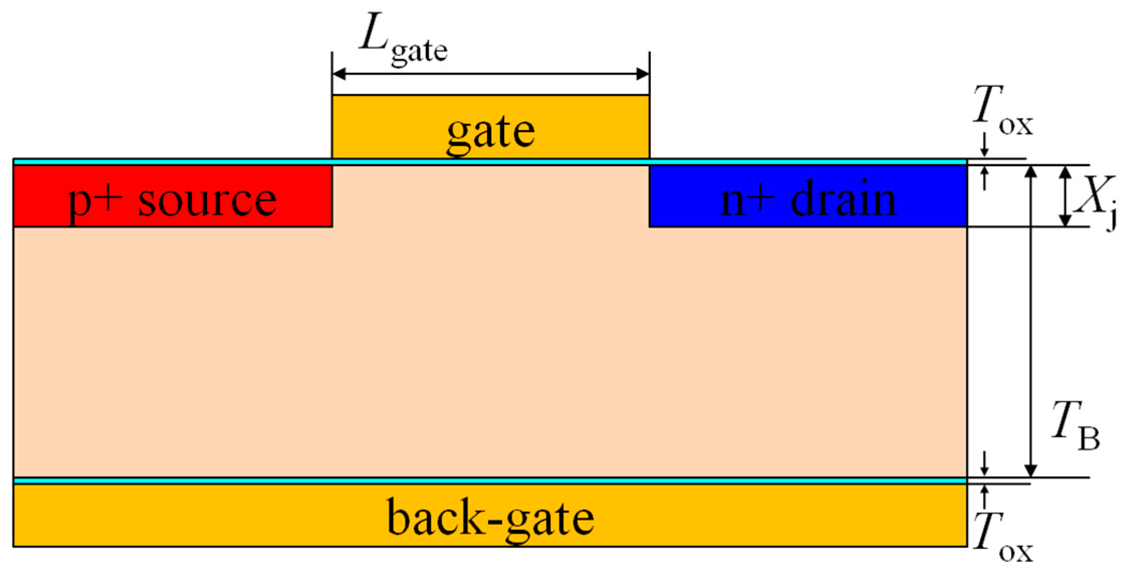
2. Simulation Conditions

The device structure studied in this work is shown in Figure 1. In order to improve current drivability with the help of pseudo-direct band-to-band tunneling (BTBT) model, a p-type source and a channel are made of Ge [9]. On the other hand, a Si drain is used for suppressing a leakage current due to the ambipolar behavior (Iamb) and the Shockley–Read–Hall (SRH) recombination observed in TFETs. As well as the top-gate oxide of a 1 nm thick SiO2 layer, the back-gate electrode is also separated from the Ge channel, using the same thickness of SiO2 to prevent the substrate leakage current, through the forward-biased source to the substrate junction; in this case, the substrate is negatively biased. The work functions for both the top and back gates are 4.05 eV. The other device design parameters are summarized in Table 1. In order to rigorously examine the BTBT behavior, a dynamic nonlocal BTBT model was used for TCAD simulation after calibration [11,12]. In addition, both indirect and direct BTBTs were considered in this simulation [7,9,11].

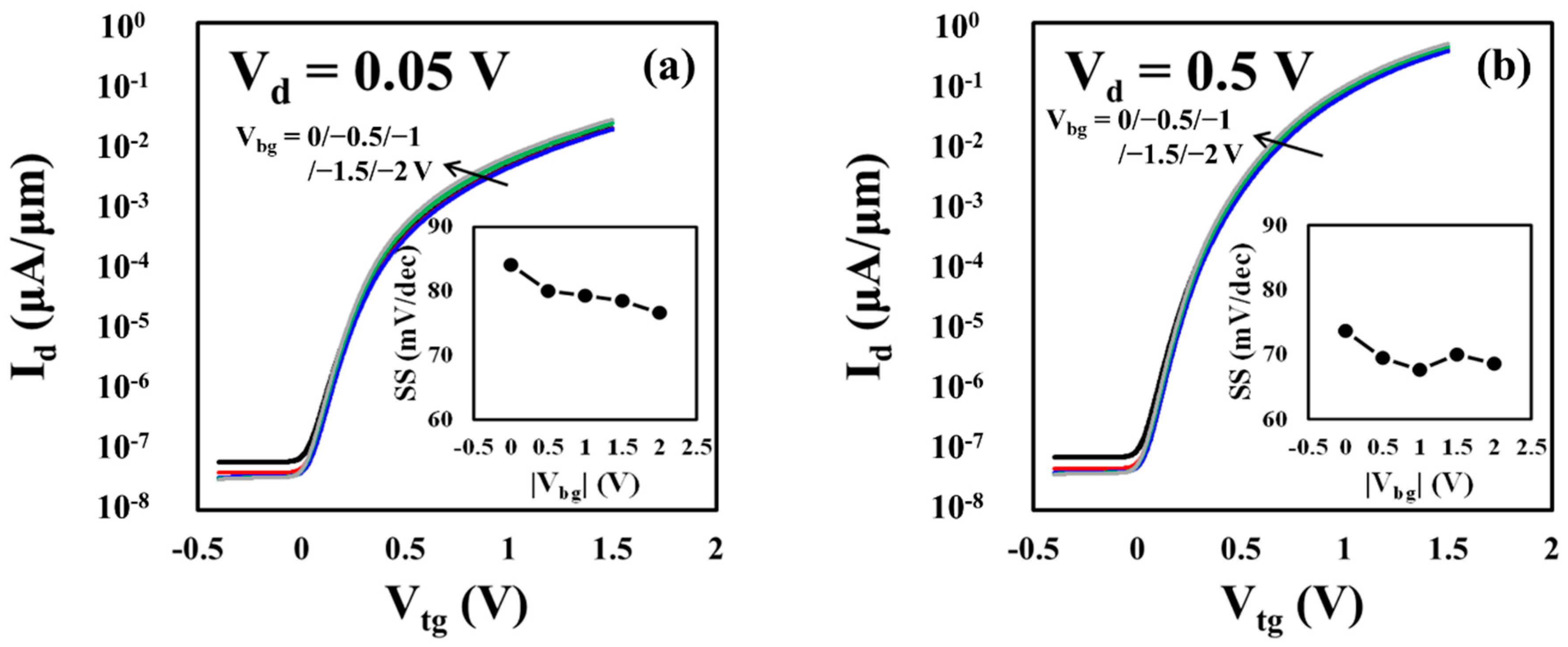
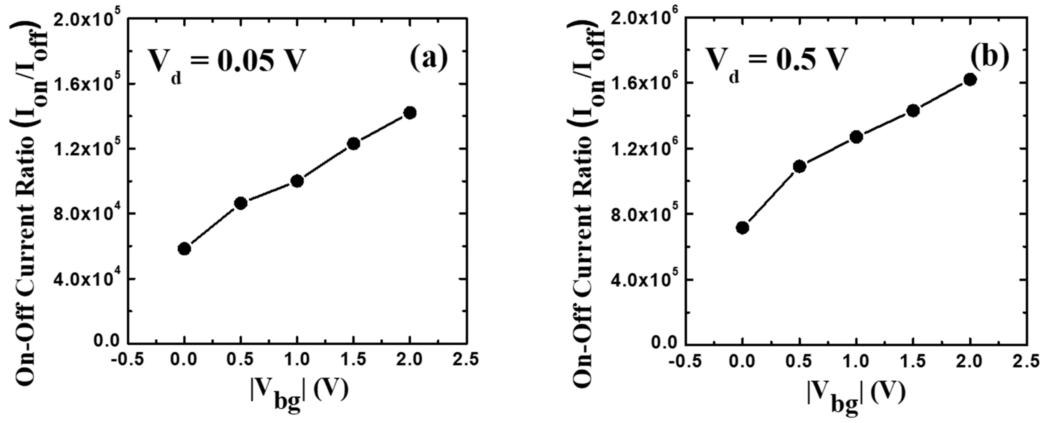
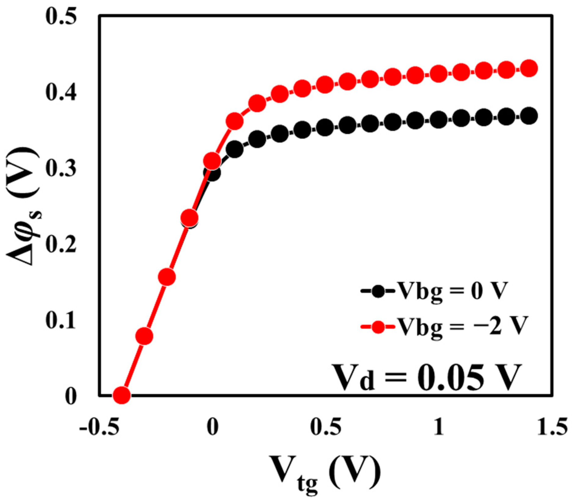
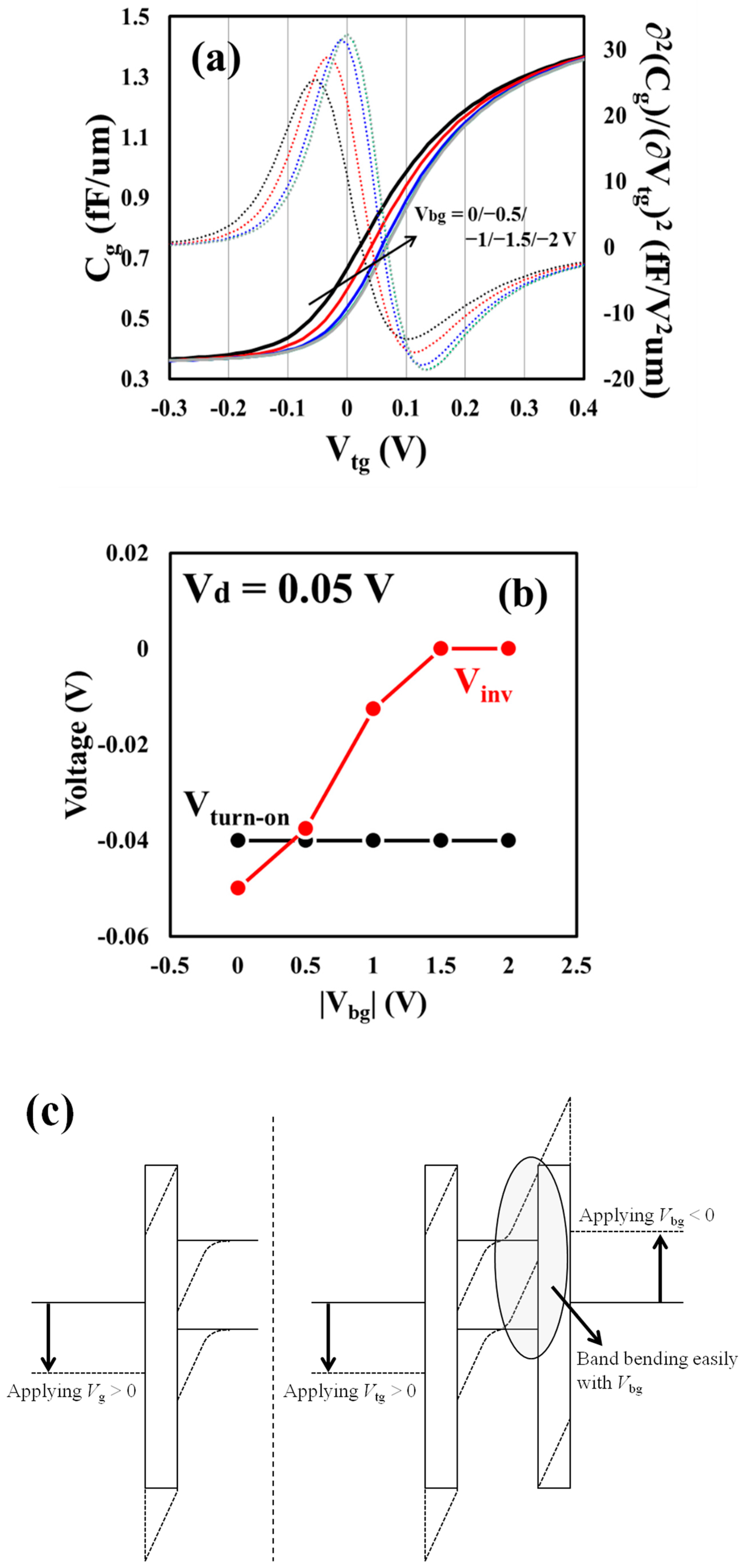
3. Results and Discussions

Figure 2 shows drain current (Id) as a function of top-gate voltage (Vtg) for different values of Vbg. Different drain voltages (Vds) of 0.05 V and 0.5 V were applied as shown in Figure 2a,b, respectively. Two noteworthy phenomena were discussed below.
First, a comparison of Figure 2a,b clarified that a higher Vds contributed to a lower minimum S. Furthermore, it was also observed that, as Vds increased, the channel inversion voltage (Vinv) increased. Vinv is defined as the value of Vtg required for the formation of an inversion layer [9]. It was observed that, similar to those of MOSFETs, the surface potential of the TFET rarely changed after an occurrence of channel inversion (VtgVinv). However, it was observed that the Vinv of the TFET was unaffected by the gate-to-source voltage (Vgs), but it was determined by the gate-to-drain voltage (Vgd) instead. Moreover, an increase in Vds also increased Vinv, while the change in turn-on voltage (Von) was negligible during the first occurrence of the BTBT. Due to this, the gate-to-channel coupling for high Vds was stronger than that for low Vds, which further resulted in a smaller S compared with that for low Vds.
Second, the insets of both Figure 2a,b indicate that S was improved as the amount of Vbg increased. As shown, if the amount of Vbg was increased up to 2 V, S was decreased from 84 to 77 mV/dec for Vds = 0.05 V and from 74 to 68 mV/dec for Vds = 0.5 V. In addition, Figure 3a,b depict the change in ratio (Ion/Ioff) of the on-state current (Ion) and the off-state current (Ioff) with increasing amount of Vbg. The Ion and Ioff are defined as Id at Vtg = 1.0 V and Vtg = 0 V, respectively. As mentioned earlier, due to the improved S by increasing the amount of Vbg, the Ion/Ioff increased by 144% and 126% for Vds of 0.05 and 0.5 V, respectively.
In order to analyze these phenomena, the change in surface potential (Δφs) of the back-gated TFET as a function of Vtg was examined, as shown in Figure 4. Δφs was extracted as the change in surface potential with respect to Vtg sweep starting from −0.4 V. As shown, for small values of Vtg, the surface potential was linearly proportional to it. However, as Vtg further increased, the surface potential became saturated. This behavior is attributed to the formation of an inversion layer, which decouples the Vtg with the surface potential [13]. Owing to the screening of the Vtg by the inversion charges at the channel, the surface potential could not be increased any further. As a result, the BTBT barrier width (i.e., BTBT probability) was almost fixed, and Id became slightly saturated, which resulted in a distinct degradation of S with the increase in Vtg, as shown in Figure 2. An interesting phenomenon observed in Figure 4 is that the saturation point of the surface potential was pulled back when Vbg was applied. The channel potential was well-controlled by Vtg before the saturation region, which explained the improvement in S with a larger |Vbg|.
In order to confirm the dependence of S on Vbg more quantitatively, the values of Vinv were extracted from the gate capacitance (Cg) and Vtg relationship for different values of Vbg, as shown in Figure 5a, and were further compared with Von, as shown in Figure 5b. By referring to [14], the values of Vinv were extracted from the first extremums of the second derivative of the CgVtg curves. The extraction method is a concept of extracting the Vth of an MOESFET similar to the maximum transconductance (gm,max) method; and the extraction equation was written as below:
d g m d V tg = d 2 I d d V tg 2 d 2 C g d V tg 2 .
As a result, the larger extremum points were obtained, when higher values of |Vbg| were applied, which meant the higher Vtg was required for the channel inversion. Because the better gate controllability was secured before the formation of the inversion layer, the higher value of Vinv means that the region of steeper transfer characteristics was expanded. The top-gate controllability improvement by the back-gate bias can be explained with the energy band diagrams of a single-gate device and a double-gate device, as shown in Figure 5c.
Considering the definitions of Vinv and Von, the mechanism of the change in S with respect to the amount of Vbg can be understood by comparing the values of Vinv and Von. As clearly observed from Figure 2a and Figure 5b, Von did not vary for different values of Vbg, and the transistor was turned on for the same value of Vtg (−0.04 V). Since the energy level of the Γ valley of Ge for direct tunneling is 0.14 eV higher than that of the L valley, where indirect tunneling occurred, it is necessary to change the surface potential, even after the turn-on point of the transistor Von, in order to improve S using direct tunneling. In the absence of Vbg, Vinv was found to be lower than Von, as shown in Figure 5b. This meant that, in this case, it was hard for direct tunneling to take place, because of the already formed inversion layer, which screened the electric field. In contrast, when a negative Vbg was applied, Vinv became larger, while Von remained the same, as shown in Figure 5b. Therefore, the direct tunneling between the source and the channel became dominant after the turn-on point of the transistor. Moreover, S was kept at a low level, until the coupling between the Vtg and the surface potential became weaker due to the formation of the inversion layer. As a result, the voltage window between Von and Vinv was found to be the determining factor for the subthreshold characteristics of TFETs. Furthermore, this is the reason why a lower S can be obtained in back-gated TFETs compared to that in conventional TFETs.

4. Conclusions

In this study, using the TCAD simulation, it was confirmed that the subthreshold characteristics of a TFET can be improved by introducing a back-gate bias, compared to those of conventional TFETs. The impact of Vbg on S was discussed using the concepts of Von and Vinv. A Vbg value of −2 V can help reduce S of the TFET with Lgate = 50 nm. For Vds = 0.05 V, an improvement in S by −7 mV/dec was achieved. In addition, the minimum S value of 68 mV/dec was obtained at Vds = 0.5 V for Vbg = −2 V. Moreover, an improvement in transfer characteristics, which was caused by the back-gate voltage, was confirmed by an increase of 126% in on–off current ratio at Vds = 0.5 V for Vbg = −2 V. Considering the applications of TFETs as a low-power device, the back-gated TFET structure can be one of the strategies for achieving better performance.

Author Contributions

Conceptualization, S.K.; data curation, J.L.; investigation, J.L.; validation, G.K.; visualization, G.K.; writing of the original draft preparation, J.L.; writing of review and editing, G.K. and S.K.

Funding

This research was supported in part by the Brain Korea 21 Plus Project, in part by the the MOTIE/KSRC under grant number 10080575 (Future Semiconductor Device Technology Development Program), in part by the NRF of Korea funded by the Ministry of Science and ICT (MSIT), Korea under grant number NRF-2019M3F3A1A03079739 (Intelligent Semiconductor Technology Development Program), in part by the MSIT, Korea, under the Information Technology Research Center (ITRC) support program (IITP-2019-2016-0-00309) supervised by the IITP (Institute for Information & communications Technology Planning & Evaluation), and in part by 2019 Research Fund of Myongji University. The EDA tool was supported by the IC Design Education Center (IDEC), Korea.

Conflicts of Interest

The authors declare no conflicts of interest.

References

  1. Hoefflinger, B. ITRS: The International Technology Roadmap for Semiconductors. In Chips 2020; Springer: Berlin, Germany, 2011; pp. 161–174. [Google Scholar]
  2. Crupi, G.; Schreurs, D.M.M.-P.; Caddemi, A. Effects of Gate-Length Scaling on Microwave MOSFET Performance. Electronics 2017, 6, 62. [Google Scholar] [CrossRef]
  3. Crupi, G.; Schreurs, D.M.-P.; Raskin, J.-P.; Caddemi, A. A comprehensive review on microwave FinFET modeling for progressing beyond the state of art. Solid-State Electron. 2013, 80, 81–95. [Google Scholar] [CrossRef]
  4. Hu, C.; Patel, P.; Bowonder, A.; Jeon, K.; Kim, S.H.; Loh, W.Y.; Kang, C.Y.; Oh, J.; Majhi, P.; Javey, A.; et al. Prospect of tunneling green transistor for 0.1V CMOS. In Proceedings of the 2010 International Electron Devices Meeting, San Francisco, CA, USA, 6–8 December 2010. [Google Scholar] [CrossRef]
  5. Choi, W.Y.; Park, B.-G.; Lee, J.D.; Liu, T.-J.K. Tunneling Field-Effect Transistors (TFETs) With Subthreshold Swing (SS) Less Than 60 mV/dec. IEEE Electron Device Lett. 2007, 28, 743–745. [Google Scholar] [CrossRef]
  6. Kim, S.W.; Kim, J.H.; Liu, T.-J.K.; Choi, W.Y.; Park, B.-G. Demonstration of L-Shaped Tunnel Field-Effect Transistors. IEEE Trans. Electron Devices 2016, 63, 1774–1778. [Google Scholar] [CrossRef]
  7. Krishnamohan, T.; Kim, D.; Raghunathan, S.; Saraswat, K. Double-Gate Strained-Ge Heterostructure Tunneling FET (TFET) With record high drive currents and ≪60mV/dec subthreshold slope. In Proceedings of the 2008 IEEE International Electron Devices Meeting, San Francisco, CA, USA, 15–17 December 2008. [Google Scholar] [CrossRef]
  8. Kim, M.; Wakabayashi, Y.; Nakane, R.; Yokoyama, M.; Takenaka, M.; Takagi, S. High Ion/Ioff Ge-source ultrathin body strained-SOI tunnel FETs. In Proceedings of the 2014 IEEE International Electron Devices Meeting, San Francisco, CA, USA, 15–17 December 2014. [Google Scholar] [CrossRef]
  9. Kim, S.W.; Choi, W.Y. Hump Effects of Germanium/Silicon Heterojunction Tunnel Field-Effect Transistors. IEEE Trans. Electron Devices 2016, 63, 2583–2588. [Google Scholar] [CrossRef]
  10. Guo, A.; Matheu, P.; Liu, T.-J.K. SOI TFET ION/IOFF enhancement via back biasing. IEEE Trans. Electron Devices 2011, 58, 3283–3285. [Google Scholar] [CrossRef]
  11. Kao, K.-H.; Verhulst, A.S.; Vandenberghe, W.G.; Soree, B.; Groeseneken, G.; De Meyer, K. Direct and Indirect Band-to-Band Tunneling in Germanium-Based TFETs. IEEE Trans. Electron Devices 2011, 59, 292–301. [Google Scholar] [CrossRef]
  12. Synopsys, Inc. Sentaurus Device User Guide; Synopsys, Inc.: Mountain View. Available online: http://www.sentaurus.dsod.pl/manuals/data/sdevice_ug.pdf (accessed on 26 November 2019).
  13. Lee, W.; Choi, W. Influence of Inversion Layer on Tunneling Field-Effect Transistors. IEEE Electron Device Lett. 2011, 32, 1191–1193. [Google Scholar] [CrossRef]
  14. Wong, H.-S.; White, M.H.; Krutsick, T.J.; Booth, R.V. Modeling of transconductance degradation and extraction of threshold voltage in thin oxide MOSFET’s. Solid-State Electron. 1987, 30, 953–968. [Google Scholar] [CrossRef]
Figure 1. Schematic diagram of a back-gated tunnel field-effect transistor (TFET).
Electronics 08 01415 g001
Figure 2. Transfer characteristics, where Vbg is changed from 0 to −2.0 V with a −0.5 V step at different Vds values: (a) 0.05 V and (b) 0.5 V. The insets are the extracted minimum S as a function of Vbg.
Electronics 08 01415 g002
Figure 3. The change in the ratio of the on-state current (Ion) and the off-state current (Ioff), where Vbg is changed from 0 to −2.0 V with a −0.5 V step, at different Vds values: (a) 0.05 V and (b) 0.5 V.
Electronics 08 01415 g003
Figure 4. The change in surface potential as a function of Vtg, when Vbg is biased by 0 and −2 V. At a higher Vtg, an increase in amount of Vbg causes the formation of an inversion layer, which results in the occurrence of the saturation of the surface potential.
Electronics 08 01415 g004
Figure 5. (a) Extraction of Vinv from the CgVtg relationship and its second derivative charts, when the Vbg is increased. Vbg slows down the inversion point. (b) Von and Vinv as a function of Vbg. Vinv increases, as the amount of Vbg increases, while Von is kept constant. (c) Energy band diagrams of a single-gate device and a double-gate device. The left diagram represents the energy band diagram of the single-gate device, and the right one represents that of the double-gate device. The negative back-gate bias of the double-gate device helps invoke band bending easily.
Electronics 08 01415 g005
Table 1. Device parameters used in technology computer-aided design (TCAD) simulation.
ParameterDescriptionUnitValue
Lgategate lengthnm50
Toxequivalent oxide thicknesses of top- and back-gate oxidesnm1
Xjjunction depthnm10
TBbody thicknessnm50
NSsource doping concentration/cm31020
NDdrain doping concentration/cm31020
NBbody doping concentration/cm31017

