Area-Efficient Pipelined FFT Processor for Zero-Padded Signals


Abstract
:1. Introduction
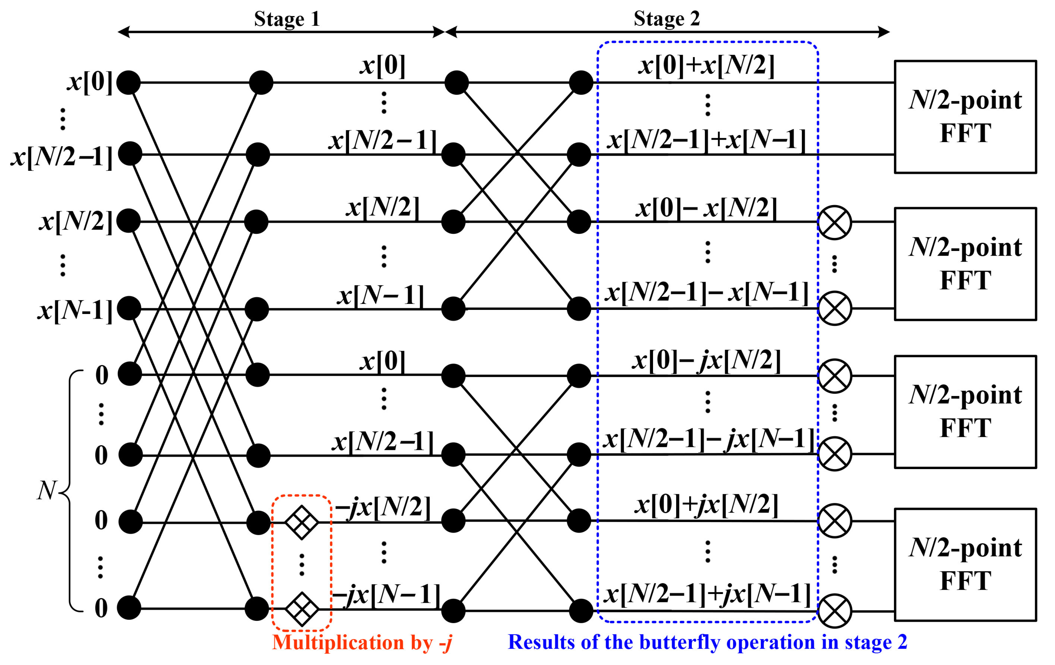
2. Zero-Padded FFT
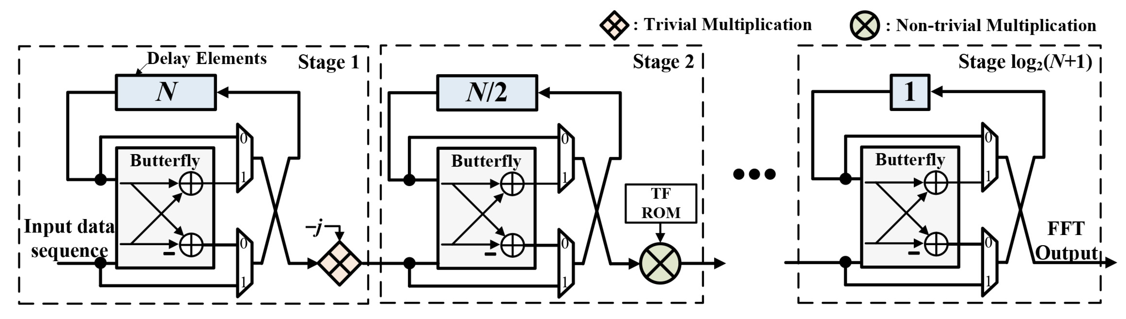
3. Proposed Hardware Architecture
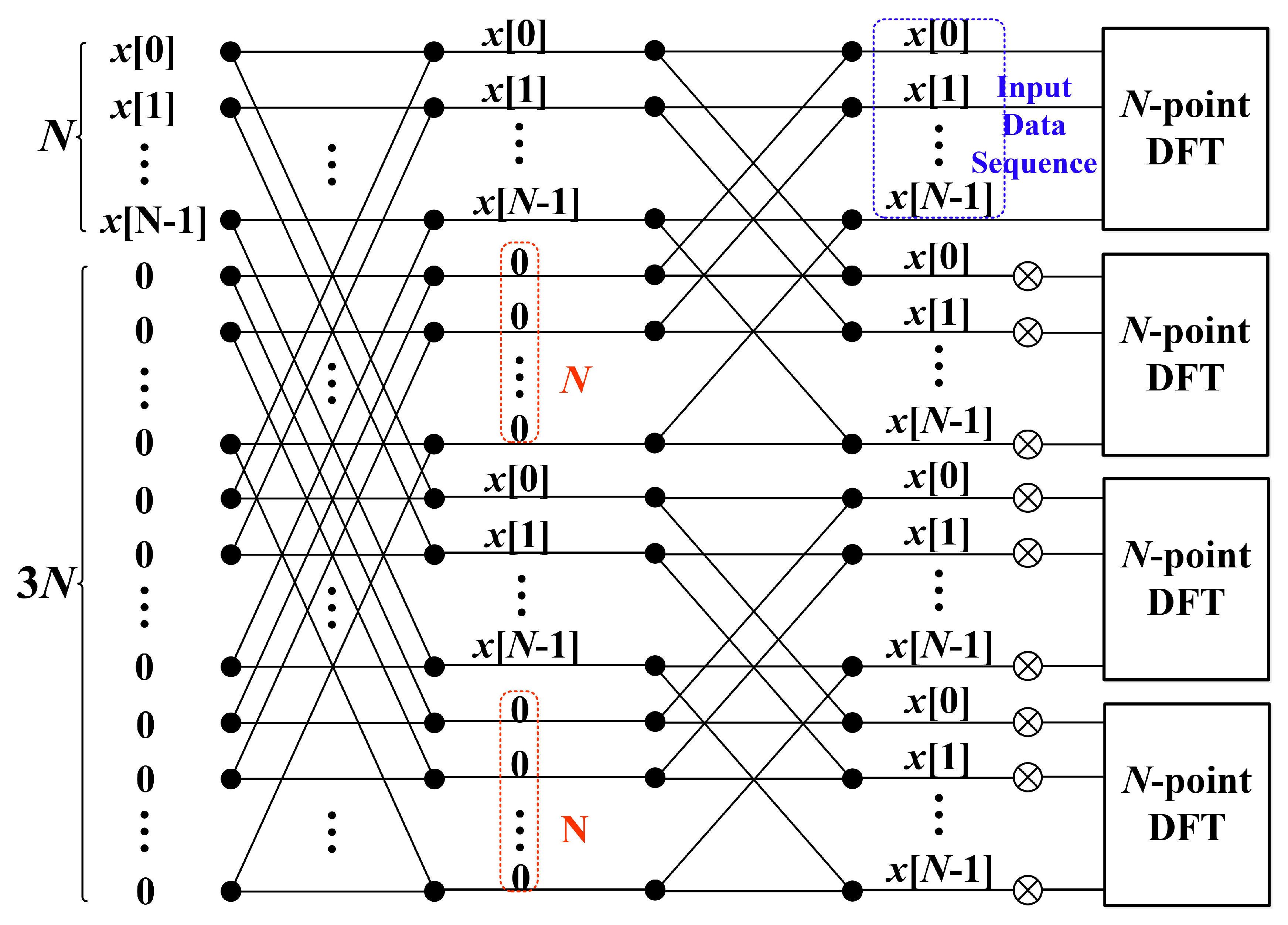
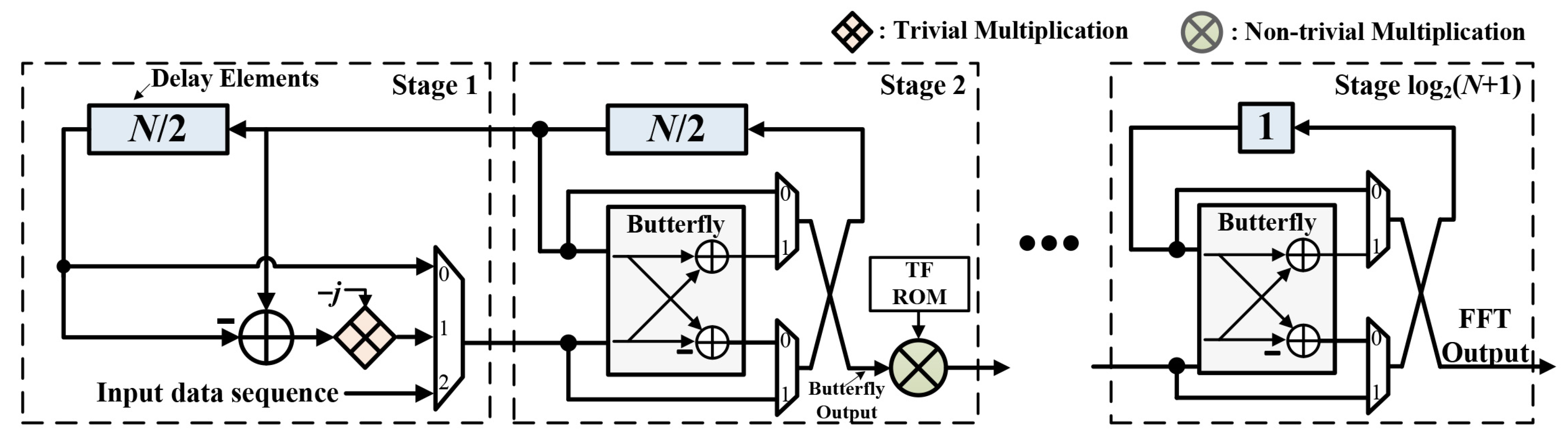
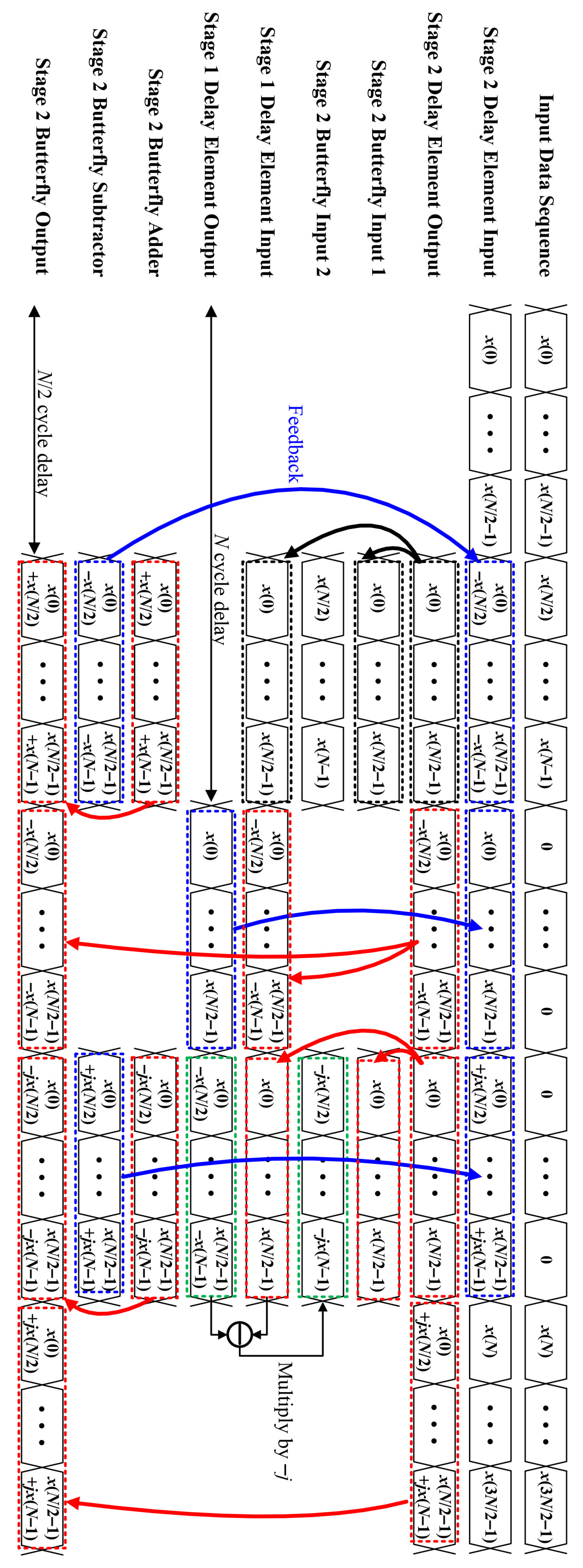
3.1. Double Frequency Resolution
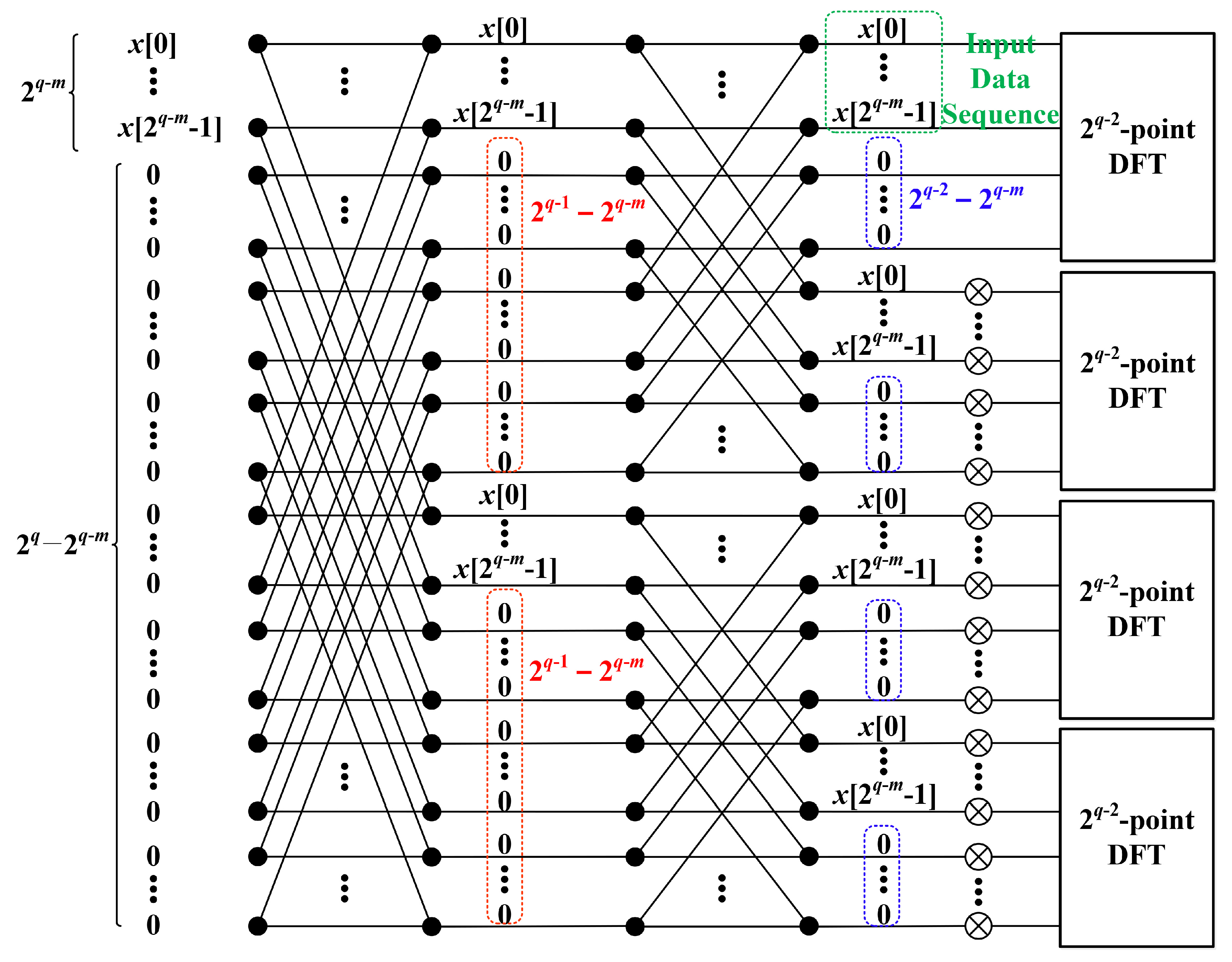
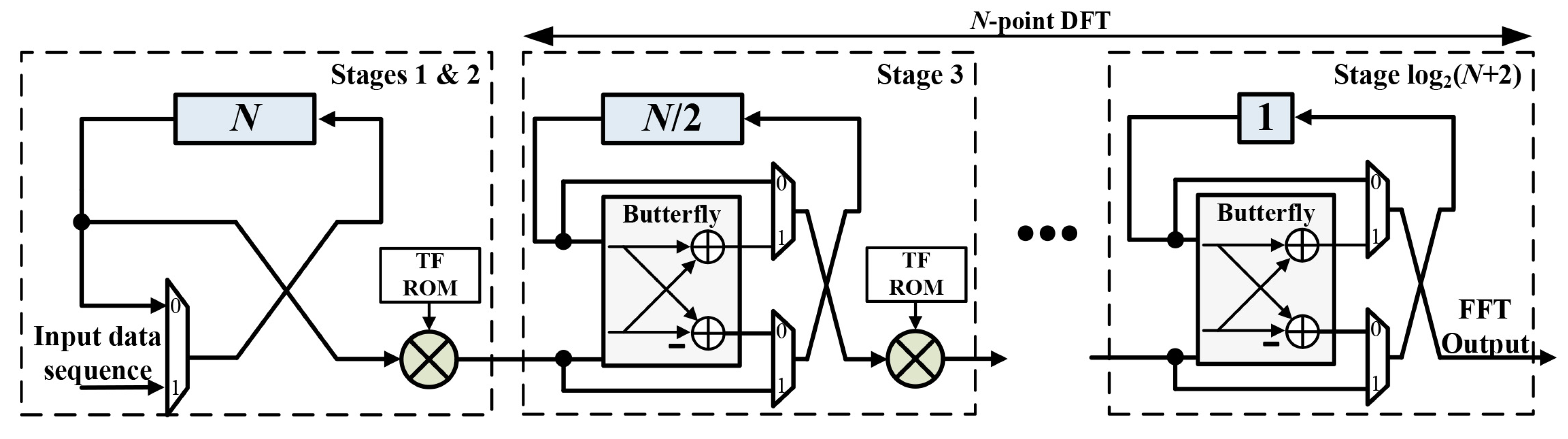
3.2. Four-Times Frequency Resolution
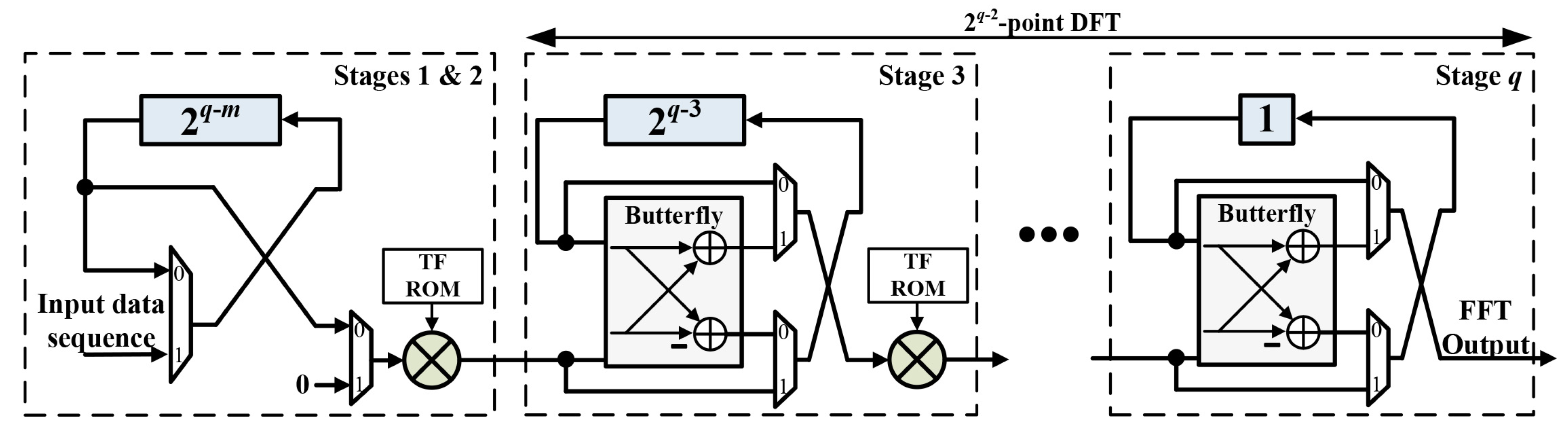
3.3. 2-Times Frequency Resolution
4. Comparison
5. Conclusions
Author Contributions
Funding
Conflicts of Interest
References
- Schafer, R.W.; Oppenheim, A.V. Discrete-Time Signal Processing; Prentice Hall: Englewood Cliffs, NJ, USA, 2009. [Google Scholar]
- Lai, S.C.; Lei, S.F.; Chang, C.L.; Lin, C.C.; Luo, C.H. Low Computational Complexity, Low Power, and Low Area Design for the Implementation of Recursive DFT and IDFT Algorithms. IEEE Trans. Circuits Syst. II Exp. Briefs 2009, 56, 647–651. [Google Scholar] [CrossRef]
- Kanatov, I.; Kaplun, D.; Butusov, D.; Gulvanskii, V.; Sinitca, A. One Technique to Enhance the Resolution of Discrete Fourier Transform. Electronics 2019, 8, 330. [Google Scholar] [CrossRef]
- Athaudage, C.R.N.; Angiras, R.R.V. Sensitivity of FFT-Equalised Zero-Padded OFDM Systems to Time and Frequency Synchronisation Errors. IEE Proc. Comm. 2005, 152, 945–951. [Google Scholar] [CrossRef]
- Liu, S.; Liu, D. A High-Flexible Low-Latency Memory-Based FFT Processor for 4G, WLAN, and Future 5G. IEEE Trans. VLSI Syst. 2019, 27, 511–523. [Google Scholar] [CrossRef]
- Minotta, F.; Jimenez, M.; Rodriguez, D. Automated Scalable Address Generation Patterns for 2-Dimensional Folding Schemes in Radix-2 FFT Implementations. Sensors 2018, 7, 33. [Google Scholar]
- Hyun, E.; Jin, Y.; Lee, J. A pedestrian Detection Scheme Using a Coherent Phase Difference Method Based on 2D Range-Doppler FMCW Radar. Sensors 2016, 16, 124. [Google Scholar] [CrossRef]
- Tang, S.; Chen, Y. Area-Efficient FFT Kernel with Improved Use of GI for Multistandard MIMO-OFDM Applications. Appl. Sci. 2019, 9, 2877. [Google Scholar] [CrossRef]
- Guoqing, Q. High accuracy range estimation of FMCW lwvel radar based on the phase of the zero-padded FFT. In Proceedings of the 7th International Conference on Signal Processing, Beijing, China, 31 August–4 September 2004; pp. 2078–2081. [Google Scholar]
- Sansaloni, T.; Perez-Pascual, A.; Torres, V.; Valls, J. Efficient pipeline FFT processors for WLAN MIMO-OFDM systems. IET Electorn. Lett. 2005, 41, 1043–1044. [Google Scholar] [CrossRef]
- Ayinala, M.; Parhi, K.K. Parallel-Pipelined Radix-22 FFT Architecture for Real Valued Signals. In Proceedings of the 2010 Conference Record of the Forty Fourth Asilomar Conference on Signals, Systems and Computers, Pacific Grove, CA, USA, 7–10 November 2010; pp. 1274–1278. [Google Scholar]
- Jung, Y.; Yoon, H.; Kim, J. New Efficient FFT Algorithm and Pipeline Implementation Results for OFDM/DMT Applications. IEEE Trans. Consum. Electron. 2003, 49, 14–20. [Google Scholar] [CrossRef]
- Yin, X.; Yu, F.; Ma, Z. Resource-Efficient Piplined Architectures for Radix-2 Real-Valued FFT with Real Datapaths. IEEE Trans. Circuits Syst. II Exp. Briefs 2016, 63, 803–807. [Google Scholar] [CrossRef]
- He, S.; Torkelson, M. Design and Implementation of a 1024-point Pipeline FFT Processor. In Proceedings of the IEEE 1998 Custom Integrated Circuits Conference, Santa Clara, CA, USA, 14 May 1998; pp. 131–134. [Google Scholar]
- Sreenivas, T.V.; Rao, P.V.S. High resolution narrow-band spectra by FFT pruning. IEEE Trans. Acoust. Speech Signal Process. 1980, 28, 254–257. [Google Scholar] [CrossRef]
- Gan, R.G.; Eman, K.F.; Wu, S.M. An extended FFT algorithm for ARMA spectral estimation. IEEE Trans. Acoust. Speech Signal Process. 1984, 32, 168–170. [Google Scholar] [CrossRef]
- Nagai, K. Pruning the decimation-in-time FFT algorithm with frequency shift. IEEE Trans. Acoust. Speech Signal Process. 1986, 34, 1008–1010. [Google Scholar] [CrossRef]
- Qin, D.Z.; Ren, J.A.; Xu, Y.H. An Efficient Pruning Algorithm for IFFT/FFT Based on NC-OFDM in 5G. In Proceedings of the 2018 Second International Conference on Inventive Communication and Computational Technologies (ICICCT), Coimbatore, India, 20–21 April 2018; pp. 432–435. [Google Scholar]
- Airoldi, R.; Garzia, F.; Nurmi, J. Efficient FFT pruning algorithm for non-contiguous OFDM systems. In Proceedings of the 2011 Conference on Design and Architectures for Signal and Image Processing, Tampere, Finland, 2–4 November 2011; pp. 1–6. [Google Scholar]
- Yuan, L.; Tian, X.; Chen, Y. Pruning split-radix FFT with time shift. In Proceedings of the 2011 International Conference on Electronics, Communications and Control (ICECC), Ningbo, China, 9–11 September 2011; pp. 1581–1586. [Google Scholar]
- Ingemarsson, C.; Kllstrm, P.; Qureshi, F.; Gustafsson, O. Efficient FPGA Mapping of Pipeline SDF FFT Cores. IEEE Trans. VLSI Syst. 2017, 25, 2486–2497. [Google Scholar] [CrossRef]
- Wang, Z.; Liu, X.; He, B.; Yu, F. A Combined SDC-SDF Architecture for Normal I/O Pipelined Radix-2 FFT. IEEE Trans. Very Large Scale Integr. Syst. 2015, 23, 973–977. [Google Scholar] [CrossRef]
- Li, J.; Liu, F.; Long, T.; Mao, E. Research on pipeline R22SDF FFT. In Proceedings of the IET International Radar Conference, Gulin, China, 20–22 April 2009; pp. 1–5. [Google Scholar]
- Lee, S.; Park, S. Modified SDF Architecture for Mixed DIF/DIT FFT. In Proceedings of the 2007 IEEE International Symposium on Circuits and Systems, New Orleans, LA, USA, 27–30 May 2007; pp. 2590–2593. [Google Scholar]
- Chang, Y.N. An Efficient VLSI Architecture for Normal I/O Order Pipeline FFT Design. IEEE Trans. Circuits Syst. II Exp. Briefs 2008, 55, 1234–1238. [Google Scholar] [CrossRef]
- Nguyen, H.N.; Khan, S.A.; Kim, C.; Kim, J. A Pipelined FFT Processor Using an Optimal Hybrid Rotation Scheme for Complex Multiplication: Design, FPGA Implementation and Analysis. Electronics 2018, 7, 137. [Google Scholar] [CrossRef]
- Gasior, M.; Gonzales, L. Improving FFT Frequency Measurement Resolution by Parabolic and Gaussian Spectrum Interpolation. In Proceedings of the 2004 Beam Instrum. Workshop, Geneva, Switzerland, 10 November 2004; Volume 732, pp. 276–285. [Google Scholar]
- Aamir, K.M.; Maud, M.A.; Loan, A. On Cooley-Tukey FFT Method for Zero Padded Signals. In Proceedings of the IEEE Symp. Emerging Technologies, Islamabad, Pakistan, 18 September 2005; pp. 41–45. [Google Scholar]
- Quinn, B.G. Recent Advances in Rapid Frequency Estimation. Digit. Signal Process. 2009, 19, 942. [Google Scholar] [CrossRef]
- Bai, Y.; Zhang, X. An Algorithm of Fast Interpolation. In Proceedings of the IEEE World Congress on Computer Science and Information Engineering, Los Angeles, CA, USA, 31 March–2 April 2009; pp. 588–590. [Google Scholar]
- He, S.; Torkelson, M. A new approach to pipeline FFT processor. In Proceedings of the International Conference on Parallel Processing, Honolulu, HI, USA, 12–16 August 1996; pp. 766–770. [Google Scholar]
- Kuo, J.C.; Wen, C.H.; Lin, C.H.; Wu, A.Y. VLSI design of a variable-length FFT/IFFT processor for OFDM-based communication systems. EURASIP J. Adv. Signal Process. 2003, 13, 1306–1316. [Google Scholar] [CrossRef]
- Chhatbar, T.D.; Darji, A.D. High Speed High Throughput FFT/IFFT Processor ASIC for Mobile Wi-Max. In Proceedings of the International Conference on Emerging Trends in Engineering and Technology, Najpur, India, 16–18 December 2009; pp. 402–405. [Google Scholar]
- Lee, H.Y.; Park, I.C. Balanced Binary-Tree Decomposition for Area-Efficient Pipelined FFT Processing. IEEE Trans. Circuits Syst. I Regul. Pap. 2007, 54, 889–900. [Google Scholar] [CrossRef]
- Yu, C.; Yen, M.H. Area-Efficient 128- to 2048/1536-Point Pipeline FFT Processor for LTE and Mobile WiMAX Systems. IEEE Trans. VLSI Syst. 2015, 23, 1793–1800. [Google Scholar] [CrossRef]
- Shih, X.Y.; Chou, H.R.; Liu, Y.Q. VLSI Design and Implementation of Reconfigurable 46-Mode Combined-Radix-Based FFT Hardware Architecture for 3GPP-LTE Applications. IEEE Trans. Circuits Syst. I Regul. Pap. 2018, 65, 118–129. [Google Scholar] [CrossRef]


| Pipelined Architecture | Complex Adder | Complex Multipliers | Delay Elements | Latency (Cycles) |
|---|---|---|---|---|
| SDF Radix-2 | 2 | 2 | 2 | |
| SDF Radix-4 | 4 | 2 | 2 | |
| SDF Radix-2 | 2 | 2 | 2 | |
| SDF Split Radix-2 | 2 | 2 | 2 | |
| SDC Radix-4 | 3/2 | 2 | 2 | |
| Proposed SDF Radix-2 ( : Odd/Even) | (Odd : 22+1 Even : 22) | (2) | (2) |
| Block Name | SDF Radix-2 | Proposed | Reduction (%) |
|---|---|---|---|
| Butterfly Unit | 7192 | 6293 | 12.5 |
| Non-trivial Multiplier | 13,783 | 13,783 | 0 |
| Delay Elements | 40,800 | 20,320 | 50.2 |
| Total | 61,775 | 40,396 | 34.6 |
| [33] | [34] | [35] | [36] | This Work | |
|---|---|---|---|---|---|
| FFT Length | 128–2048 | 1024–8192 | 128–2048 | 4–2048 | 256 |
| FFT Architecture | SDF | SDF | SDF | SDF | SDF |
| Frequency (MHz) | 40 | 112 | 40 | 500 | 300 |
| Word Length (Bit) | 16 | 12 | 12 | 14 | 12 |
| Technology | 180 | 180 | 90 | 40 | 65 |
| Execution Time/FFT Length @ 20MHz (ns) | 50 | 50 | N.A. | N.A. | 28 |
| Area (mm) | 6.76 | 3.52 | 0.783 | 0.36 | 0.18 |
| Normailzed Area | 80.14 | 35.31 | 37.13 | 86.42 | 22.50 |
© 2019 by the authors. Licensee MDPI, Basel, Switzerland. This article is an open access article distributed under the terms and conditions of the Creative Commons Attribution (CC BY) license (http://creativecommons.org/licenses/by/4.0/).
Share and Cite
Jung, Y.; Cho, J.; Lee, S.; Jung, Y. Area-Efficient Pipelined FFT Processor for Zero-Padded Signals. Electronics 2019, 8, 1397. https://doi.org/10.3390/electronics8121397
Jung Y, Cho J, Lee S, Jung Y. Area-Efficient Pipelined FFT Processor for Zero-Padded Signals. Electronics. 2019; 8(12):1397. https://doi.org/10.3390/electronics8121397
Chicago/Turabian StyleJung, Yongchul, Jaechan Cho, Seongjoo Lee, and Yunho Jung. 2019. "Area-Efficient Pipelined FFT Processor for Zero-Padded Signals" Electronics 8, no. 12: 1397. https://doi.org/10.3390/electronics8121397
APA StyleJung, Y., Cho, J., Lee, S., & Jung, Y. (2019). Area-Efficient Pipelined FFT Processor for Zero-Padded Signals. Electronics, 8(12), 1397. https://doi.org/10.3390/electronics8121397