1. Introduction
In the area of industrial measurement, testing, and process technology, there exist many applications of power amplifiers in order to generate current and voltage signals of special shape at high power levels. [
1,
2]. Voltage mode Class-D amplifiers (CDAs), composed of voltage source inverters with LC filters, are used to power voltage-driven loads, such as the piezoelectric ceramic transducer [
3] and the electrostrictive transducer [
4]. Commonly used inverter topologies in CDAs can be divided into three categories: the half H-bridge inverter [
5], the full H-bridge inverter [
6,
7,
8], and the cascaded H-bridge inverter [
1]. However, the used inverter topology in this paper is the full-bridge neutral-point clamped (NPC) inverter, which features lower voltage stress on power semiconductors, lower voltage harmonics, smaller electromagnetic interference compared with the half H-bridge inverter and the full H-bridge inverter [
9]. In addition, this topology costs less switch devices compared with the cascaded H-bridge. However, the closed-loop control of the output voltage is still a complex but meaningful issue when this topology and an LC filter are used together as a voltage mode Class-D amplifier. The reason can be stated as follow. First, arbitrary waveforms in a wide band may be required in the CDA [
10]. This demand requires the dynamic response of the voltage controller to be fast enough. Second, load parameters of CDAs may be complex and variable [
4,
5,
6,
7,
8,
9,
10,
11]. Then the voltage controller is also required to be robust.
In order to achieve output closed-loop control of cascaded H-bridge CDAs, a single PI voltage controller was used in [
1]. However, PI gains are required to be turned repeatedly in this method, and the steady state performance and the transient response compromise each other [
12]. In [
13], a double closed-loop PI controller, whose bandwidth was increased compared with the single PI controller in [
1], was used for cascaded H-bridge voltage mode CDAs. Limited by the dynamic performance of the existing linear controllers, nonlinear controllers, such as the sliding mode controller, was proposed in [
14,
15] for voltage mode CDAs. The sliding mode controller has better dynamic performance, but it suffers from finding out the sliding surface and the existing chattering phenomena.
As an another nonlinear controller, model predictive control (MPC) has the advantages of ability to handle multiple control objectives and constraints, simplicity and fast dynamic response, and has been widely concerned and studied in recent years. Moreover, it has been successfully applied to several multilevel inverters. In [
16], the finite control set model predictive control (FCS-MPC) was applied for the grid-tied three-phase three-level NPC inverter. In [
17], the FCS-MPC was also used to a full-bridge NPC inverter. But in [
16,
17], the output current or voltage tracking and the capacitor voltage balancing were achieved simultaneously by repeatedly predicting and evaluating the sum of the quadratic terms with weight factors in the cost function, which reflected the two control objectives, respectively. However, the repeated predicting and evaluating the complex cost function costed many computations. In [
18], the MPC based on optimal switching sequences was proposed for the full-bridge NPC inverter, which could achieve fixed switching frequency for the switch devices. However, this method failed to balance the capacitor voltage [
19]. In [
19], a low-complexity MPC was also proposed for the full-bridge NPC rectifier. Although the capacitor voltage balancing could be achieved with unbalanced loads, the fixed switching frequency still limited the dynamic performance of the MPC. In [
20,
21], the complexity of the MPC algorithm was reduced by employing the multistep MPC for modular multilevel converter (MMC) and cascaded H-bridge inverter. But the dynamic performance would also be affected. In [
22,
23], only the adjacent voltage vectors or output levels were considered for the FCS-MPC algorithm, and the required computation was reduced greatly. However, both of the dynamic response and the control accuracy would be affected under the condition of load step or reference step for these methods. In [
24,
25,
26,
27], the process of evaluating the quadratic cost function was regarded as a least square problem, and was proposed to be solved by sphere decoding algorithm or its improved algorithms. But large amount of calculation was still unavoidable for the sphere decoding algorithm.
In addition, because of the high dependence on system model, the effectiveness of the MPC faces enormous challenges when there are errors between the actual system model and the established model. This issue can also be expressed as the robustness of the MPC. The robust MPC has been studied for various power electronic converters, such as three-phase three-level NPC converters [
28], three-phase PWM rectifiers [
29], flying capacitors inverters [
30], and three-phase inverters with LC filters [
31,
32], etc. In [
28], the robustness was achieved by a weighted average process of the measured system variables and the predicted variables. Then the control error caused by the model error could be reduced. However, it failed to deal with the dynamic changes of parameters. In [
29], the robust MPC was achieved based on an online disturbance observer. But the influence of the parasitic resistances of the grid-tied inductors were not investigated in the simulation and experiment. In [
30], the system robustness was improved based on an adaptive observer. But the variation of the filter inductor was also not included. In [
31], the robustness was also achieved based on a disturbance observer. But the load current was obtained by an additional observer, which made the control system more complex. In [
32], the output of the three phase inverter prediction model at current control instant was compensated by the modeling error of the last control instant. However, only simulation results were provided, and additional current sensors were required.
In this paper, a robust two-layer MPC is proposed for the full-bridge NPC inverter based CDAs. Based on the designed Luenberger observer, the disturbances caused by both the parameter uncertainties or mismatches of the LC filter and the load current can be centrally estimated and compensated to the prediction model in each control period, which can save computation and avoid the use of load current sensor. Moreover, layered structure is used in the proposed robust MPC, so that the output voltage tracking and the capacitor voltage balancing can be achieved simultaneously and decoupled without affecting the dynamic performance, and the required computation can be further reduced.
The rest of this paper is organized as follows. In
Section 2, the discrete mathematical model of the CDA is established. In
Section 3, a Luenberger disturbance observer based on Kalman filter is designed to estimate the disturbance caused by the parameter mismatch and the load current. In
Section 4, a two-layer MPC for the voltage mode CDA is proposed.
Section 5 reports the experiment results. In
Section 6, the performance of the proposed robust two-layer MPC is focused on discussion and comparison. And the conclusions are presented in
Section 7.
2. Modeling of the Voltage Mode Amplifier Using Full-Bridge NPC Inverter
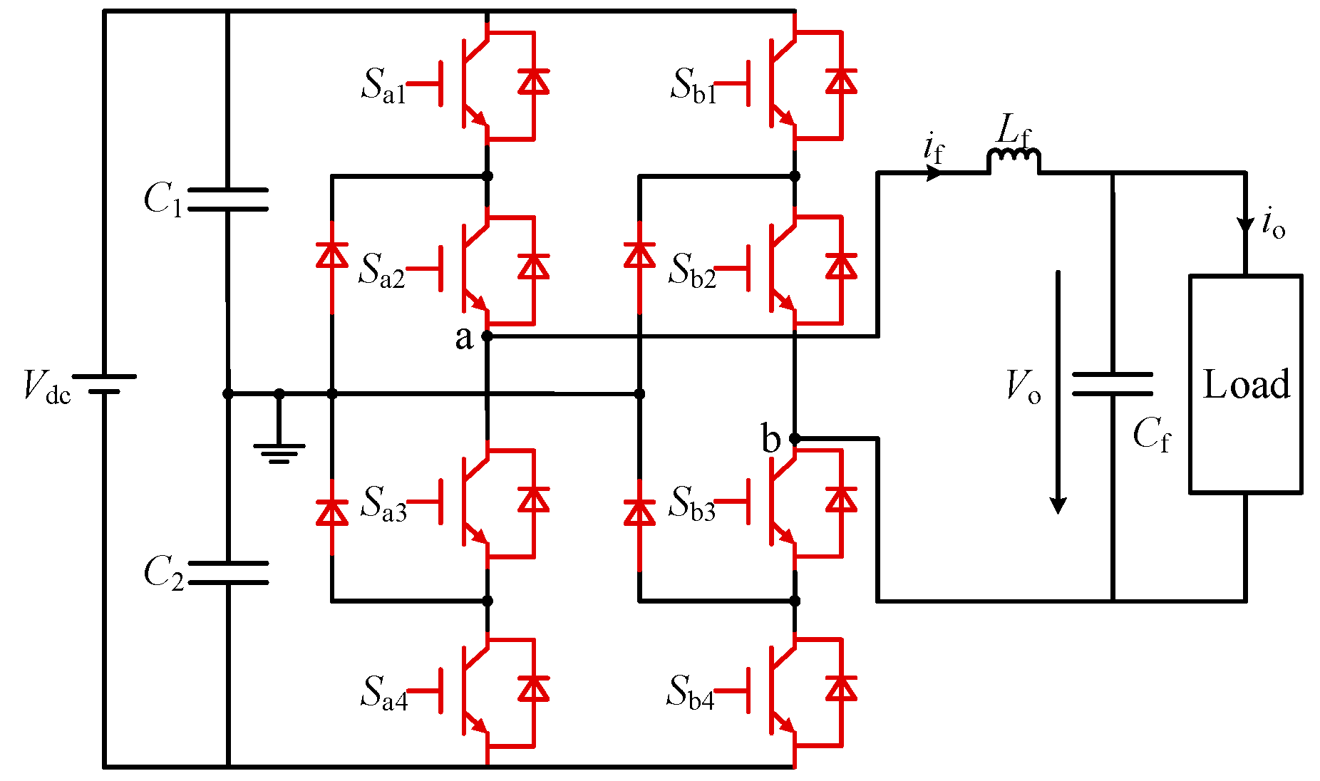
The structure of the full-bridge NPC inverter-based voltage mode Class-D amplifier is shown in
Figure 1. The filter inductor is denoted by
Lf, and the filter capacitor is denoted by
Cf. The voltage of
Cf is denoted by
Vo, which is also the final output voltage of the digital amplifier. The current of
Lf is denoted by
if, and the final output current of the digital amplifier is denoted by
io. Both the defined positive directions of
if and
io are shown in
Figure 1. The output voltage of the full-bridge NPC inverter is denoted by
Vab. The full-bridge NPC inverter consists of two bridges. Each bridge consists of four transistors with four antiparallel freewheeling diodes and two clamping diodes. The dc input is denoted by
Vdc, and two identical capacitors
C1 and
C2 are connected in series to obtain two levels of
Vdc/2 and −
Vdc/2. Driving signals of the transistors can be denoted by
Sxi.
x∈{a, b} denotes legs of the inverter, where
a denotes the left one,
b denotes the right one.
i∈{1, 2, 3, 4} denotes the number of transistor in the same bridge. In normal operation,
Sa1 and
Sa3 complement each other, and
Sa2 and
Sa4 complement each other, too.
Sb1,
Sb2,
Sb3, and
Sb4 also meet this constraint.
UC1 and
UC2 are used to represent the voltages of capacitors
C1 and
C2, respectively.
S is defined by [
Sa1 Sa2 Sa3 Sa4 Sb1 Sb2 Sb3 Sb4] and used to denote the switching state of the inverter.
M denotes the output level of the full-bridge NPC inverter. And
M∈{−2, −1, 0, 1, 2} is easy to be obtained.
Because of the limitation of the complementary driving signals mentioned above, there are only nine effective switching states, which can be denoted by S1–S9.
Table 1 shows the relationship between the output level
M, the inductor current
if, the change of
UC1, and the nine effective switching states.
Assuming that
UC1 and
UC2 are well balanced, the differential equation of the full-bridge NPC inverter-based voltage mode amplifier can be obtained as Equation (1) from
Figure 1, based on the Kirchhoff’s laws of voltage and current.
In Equation (1),
Vab can also be represented by the output level of the full-bridge NPC inverter,
M, as shown in Equation (2).
By substituting Equation (2) into Equation (1), Equation (3) can be obtained.
The filter inductor current
if and the filter capacitor voltage
Vo can be selected as the state variables of the system, and can be denoted by
x= [
if Vo]
T. Therefore, and the model of the full-bridge NPC inverter based voltage mode amplifier can be transformed into Equation (4),
where
,
,
.
For the purpose of digital control, Equation (4) should be discretized. If the sampling period and the control period are denoted as
TS, the discrete model can be expressed as Equation (5),
where
,
,
,
k and
k+1 represent the
kTS and (
k+1)
TS instant, respectively.
3. Design of the Luenberger Observer for Disturbance Estimation
Luenberger observer adopts a predictor-corrector structure. In the predictor, a predictive model is used to predict the system operation. In the corrector, a feedback signal is compensating to the predictive model to correct the error between the actual system and the used predictive model [
29]. In this paper, it is used to estimate and compensate the lumped disturbance caused by the mismatch or uncertainty of the filter parameters and the load current.
3.1. Design of the Disturbance Observer
In order to achieve robust MPC, there are two great challenges. The first one is the unknown load current io, because the load current sensor is intentionally avoided. And it will generate large disturbance for the precise control of the output voltage Vo. The second one is the uncertain parameters of the LC filter. Based on Equations (4) and (5), it can be seen that the parameter matrices Ad, B1d, and B2d are calculated from Lf and Cf, which are the actual parameters of the LC filter. However, the actual parameters Lf and Cf may not equal to the nominal parameters Lfn and Cfn, which are used in the controller. The actual parameter of the filter inductor, Lf, may not be equal to the nominal parameter Lfn, because of several phenomena, such as the magnetic saturation. And the actual parameter of the filter capacitor, Cf, may also not be equal to the nominal parameter Cfn, because of the unmodeled parasitic resistance and the manufacturing tolerance.
Both of
Lf and
Cf are difficult to obtain accurately in practical engineering. In order to distinguish the discrete model used in the controller from the actual system model, the parameter matrices used in the controller are denoted by
Adn,
B1dn, and
B2dn, and can be calculated by Equations (6)–(8) based on the nominal parameters
Lfn and
Cfn, respectively.
In (6)–(8), , , .
The relationship between the actual parameter matrices
Ad,
B1d, and
B2d and the nominal parameter matrices
Adn,
B1dn, and
B2dn can be shown in Equations (9)–(11),
where Δ
Ad, Δ
B1d, Δ
B2d denote the model errors caused by the mismatch or uncertainty of the LC filter parameters. Then the discrete system model in Equation (5) can be transformed into Equation (12) by substituting Equations (9)–(11) into (5).
In the right side of Equation (12), there are four uncertain terms. The first one is the third term
B2dnio(
k), which is uncertain because of the unknown
io(
k) in the absence of the load current sensor. The second one and the third one are the fourth term Δ
Adx(
k) and the fifth term Δ
B1dM(
k), which are uncertain because of the uncertain matrices Δ
Ad, and Δ
B1d. The fourth one is the last term Δ
B2dio(
k), which is uncertain because of both the uncertain matrix Δ
B2d and the unknown load current
io(
k). For the purpose of achieving robust control against the unknown
io(
k) and the uncertain Δ
Ad, Δ
B1d, Δ
B2d, the sum of the four terms is regarded as the lumped disturbance variable
N(
k), as shown in Equation (13).
The lumped disturbance N(k) is a two-dimensional variable, and can be expressed as N(k) = [N1(k) N2(k)]T. If both of N1(k) and N2(k) can be successfully estimated and compensated to the system predictive model based on the nominal parameters in real time, the disturbance-rejection approach can be implemented to achieve robustness against the uncertainty of the filter parameters and the load current io. And this will be still effective even if the system parameters vary during operation, which is regarded as the dynamic parameter variations.
The disturbance variables
N1(
k) and
N2(
k) can be assumed to be constant during each sampling interval [
29,
31], and they can be extended as the system variables. Then Equation (14) is obtained as,
where
,
.
And the output equation of the system can be expressed as Equation (15),
where
.
Based on Equations (14) and (15), a discrete observer can be constructed as shown in Equation (16),
where
and
respectively denote the estimated value of
X(
k) and
X(
k−1), and
L denotes the gain matrix.
M(
k−1) denotes the output level of the full-bridge NPC inverter in the (
k−1)th control period, which is obtained by the proposed two-layer MPC in the (
k−1)th control period.
can be used to denote the estimated value of
N(
k), and it can be calculated by Equation (17).
3.2. Parameter Design
The Kalman filter is a commonly used method to optimally estimate the state of a dynamic system from a series of imperfect noisy measurements, especially in presence of uncertainties [
31]. In this paper, the designed observer can be regarded as a discrete Kalman filter to calculate the observer gain matrix
L.
As an optimal recursive data processing algorithm, the discrete Kalman filter can perform cyclic calculation according to the following five steps in each control period.
The first step is to calculate the prior state estimate value
based on Equation (18).
The second step is to calculate the priori estimate error covariance matrix
based on Equation (19),
where
Q is the given process noise covariance matrix, and
Pk−1 is the posteriori estimate error covariance matrix in the last control period.
The third step is to calculate the observer gain matrix
L based on Equation (20),
where
R is the given measurement noise covariance matrix.
The fourth step is to update the estimated state variable
based on Equation (21).
The fifth step is to calculate the posteriori estimate error covariance matrix
Pk based on Equation (22).
where
I denotes the identity matrix.
The first step and the second step can be collectively referred to as the prediction link of the discrete Kalman filter. And the last three steps can be collectively referred to as the correction link of the discrete Kalman filter.
The stability of the designed discrete Kalman filter has been proved by [
31,
33], and will not be discussed here.
Remark: The performance of the designed state observer is determined by the given matrix Q and R. The larger Q is, the faster the observed values converge to their actual value, but too fast convergence speed will lead to noise interference. The smaller R is, the less noise interference, but the slower convergence rate. Therefore, Q and R should be adjusted synthetically to achieve the tradeoff between convergence speed and noise suppression.
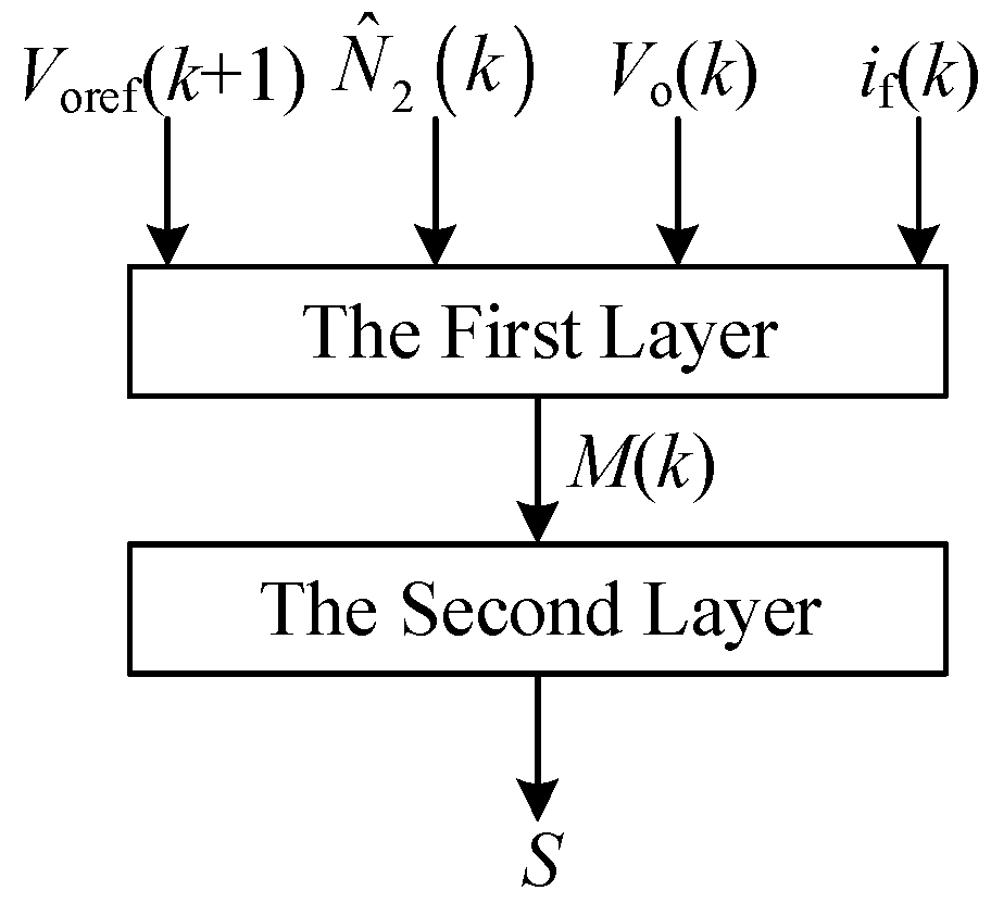
4. Two-Layer Model Predictive Control
The basic control objectives of the voltage CDA using full-bridge NPC inverter include two terms: (1) output voltage tracking; (2) capacitor voltage balancing. Traditional FCS-MPC (TFCS-MPC) requires repeated predictions and evaluations for each effective switching state, and the one which minimizes the cost function is selected as the optimal control option. Thus when it is applied to the full-bridge NPC inverter, there will be nine candidate switching states. And this places large computational burden on the digital controllers when a small control period is required.
Therefore, a two-layer MPC for the cascaded full-bridge NPC voltage mode amplifier is proposed in this paper, which is much simpler than TFCS-MPC without affecting the dynamic performance. And the proposed two-layer MPC decouples the two control objectives, which also allows the two control objectives to be achieved simultaneously without weight factors. The structure of the proposed two-layer MPC is shown in
Figure 2, where the first layer is used to calculate the optimal output level for the purpose of achieving the first control objective, the second layer is used to determine the switching state for the purpose of achieving the second control objective.
4.1. The First Layer
The reference of the output voltage can be denoted by
Voref, which is also the voltage signal to be amplified. In this system, the cost function corresponding to level
h can be defined as
J(
h) in Equation (23),
where
Voh(
k+1) denotes the output current at (
k+1)
TS instant when
h is selected in the
kth control period.
Based on Equations (12) and (13),
Voh(
k+1) can be predicted as given in Equation (24).
In Equation (24),
N2(
k) cannot be obtained because it is determined by the uncertain model errors and the unknown load current
io without configured load current sensor. However, the designed Luenburger observer can successfully estimate
N2(
k) to
, then we are allowed to replace
N2(
k) with
. Thus Equation (24) can be improved to Equation (25).
Another function,
J1(
h), with the output level
h as its independent variable can be defined by Equation (26).
The relationship between
J1(
h) and
h will be linear if
h is supposed to be continuous. For the convenience of expression, another variable,
hsol is defined as the solution of
J1(
h) = 0, and can be calculated as Equation (27).
Because of
, the optimal output level
M(
k), which minimizes
J(
h), must be equal to the integer nearest to
hsol. Thus the optimal output level
M(
k) is allowed to be directly obtained by Equation (28),
where
round(
x) denotes the rounding function, which is equal to the integer nearest to
x.
In order to avoid the case that the result of Equation (28) does not belong to
H, Equation (29) is also required after Equation (28).
Thus the cost function is evaluated only once, which greatly reduces the computational burden.
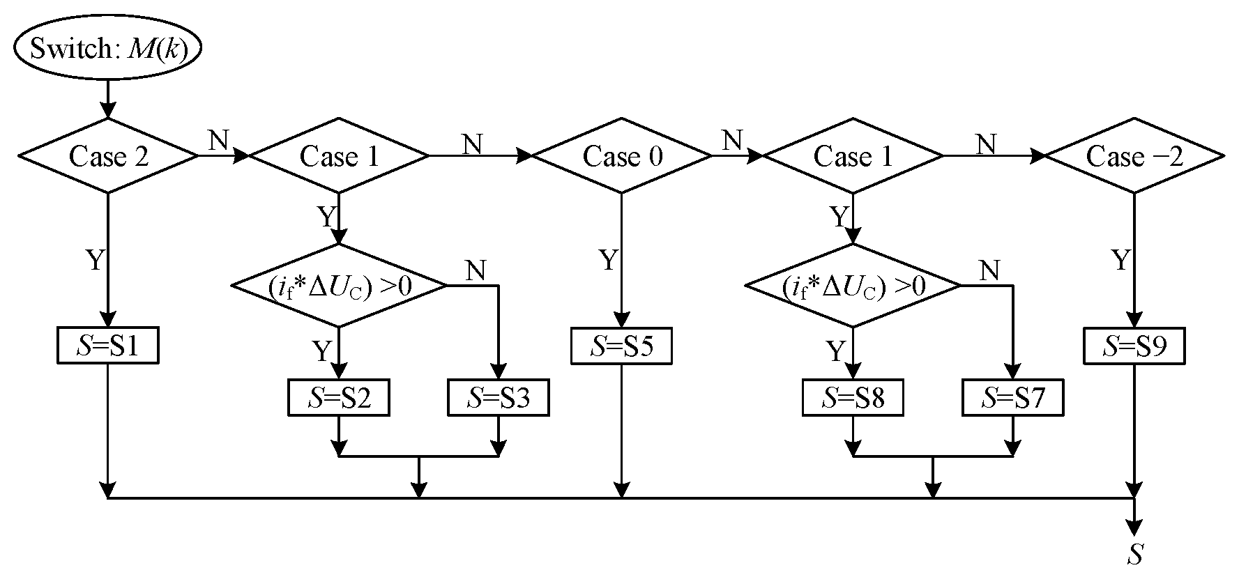
4.2. The Second Layer
The second layer is used to determine the switching state to achieve capacitor voltage balancing. At the same time, the switching action times should also be considered when the switching state is determined, because there are multiple switching states to be selected if level −1, 0, or 1 is required.
In steady-state operation, the full-bridge NPC inverter is generally switched between adjacent levels. Thus the output level will be switched between 2, 1, and 0 when
M(
k) > 0.
Table 2 shows the number of switching actions when the three levels are switched between each other. According to
Table 2, if the submodule output level is 2, the switching state can only select S1. If the submodule output level is 1, in order to achieve the purpose of capacitor voltage balance, S2 should be selected when the signs of
io and Δ
UC are the same, while S3 should be selected when they are opposite, considering the result of
Table 1. If the submodule output level is 0, the switching state can only select S5, in order to minimize the switching actions when level 0 and level 1 are switched between each other.
Similar analysis can be done when M(k) < 0 and the following conclusions can be drawn. If the submodule output level is −2, S9 is selected. If the submodule output level is −1, S8 is selected when the signs of io and ΔUC are the same, while S7 is selected when the signs of io and ΔUC are opposite. If the submodule output level is 0, S5 is selected.
Figure 3 shows the flow chart of the switching state selection process. The parallel structure of the middle and lower layer control shows that they are more suitable for implementation by a FPGA.
5. Experimental Verification
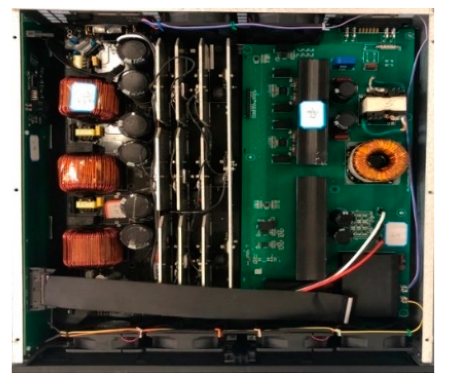
In order to verify the feasibility and validity of the proposed robust multilayer MPC applied to the full-bridge NPC voltage-mode digital power amplifier, a 2 kW experimental prototype with a 50 Hz–800 Hz output band is built in the laboratory as shown in
Figure 4. The actual value
Lf of the filter inductor used is 2 mH, and the actual value
Cf of the filter capacitor used is 10 uF. The voltage of the dc input,
Vdc, is 300 V, so that two voltage levels of 150 V and −150 V can be obtained. The capacitance of those two capacitors
C1 and
C2 is 1070 uf. The control frequency is set to be 100 kHz, which means that the sample period is set to be 10 us. The high control frequency is used because wide range output frequency and high precision out voltage are required. Thus the maximum switching frequency of the used switch devices is 50 kHz. In fact, the designed digital power amplifier uses SGH80N60UFD type fast IGBT and DSE130–60; a type fast recovery diode, whose maximum switching frequency can be up to 100 kHz.
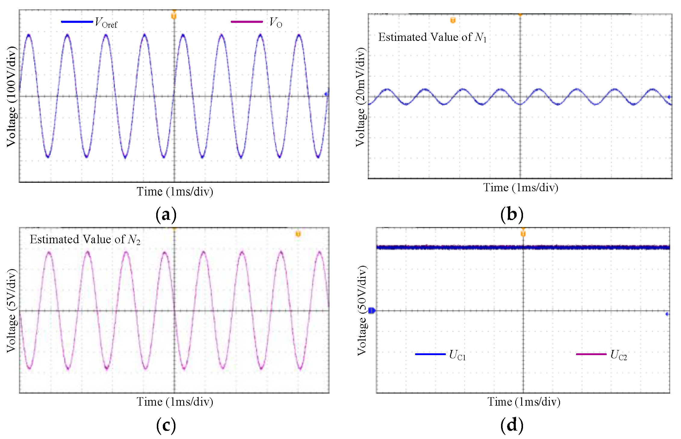
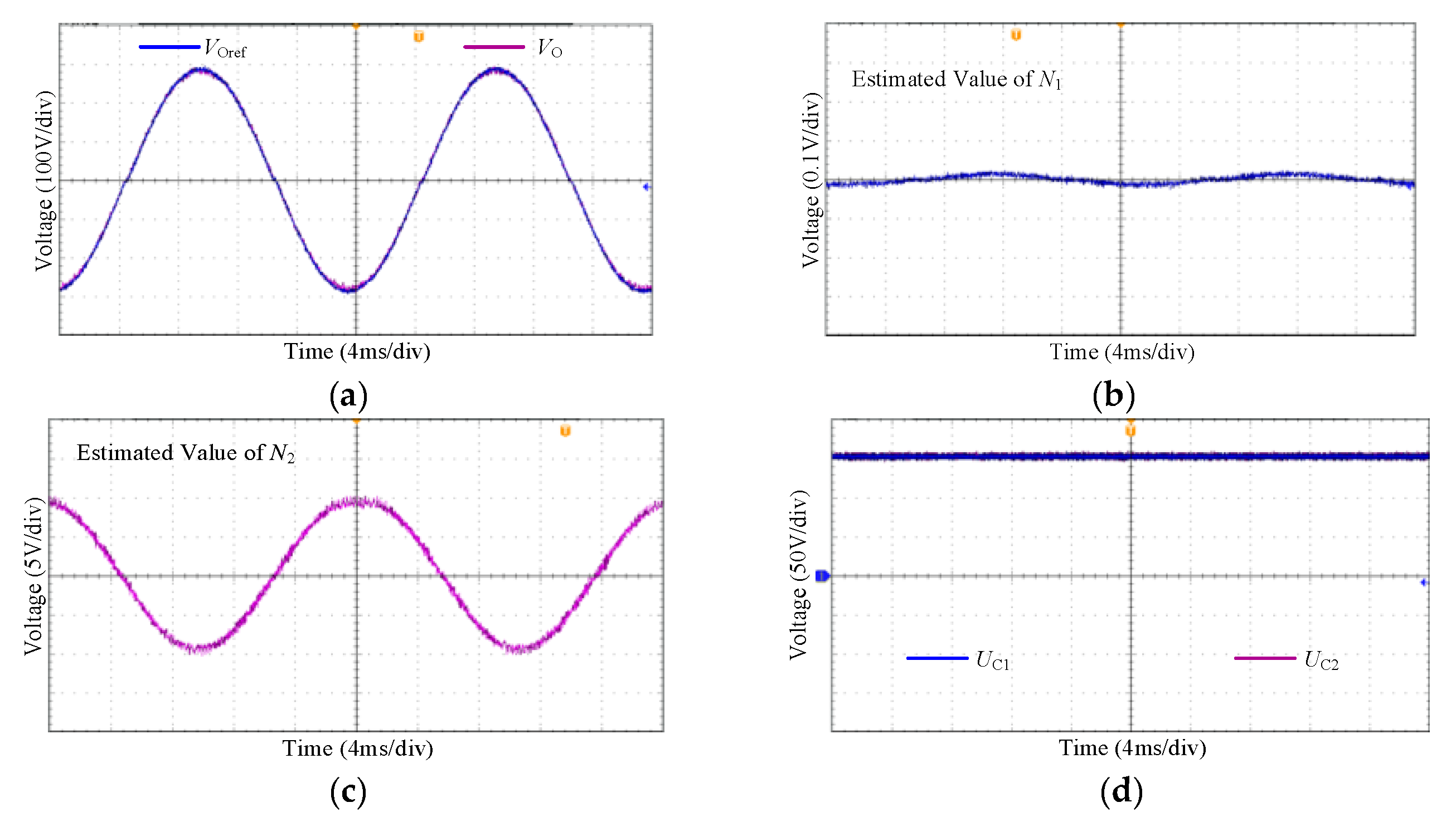
5.1. Steady State Performance
In order to study the steady state performance of the proposed RM-MPC, the output voltage reference
Voref is set to a sine wave with an 800 Hz frequency and a 200 V root-mean-square (RMS) value, which may be widely used in underwater electroacoustic transduction system. The load is set to a 20 Ω resistor. The experiment results are shown in
Figure 5, where (a) shows the waveforms of
Vo and its reference
Voref, (b) shows the waveform of the estimated value of
N1, (c) shows the waveform of the estimated value of
N2, (d) shows the waveforms of the two capacitor voltages in the dc side.
It can be seen that the output voltage is accurately tracked with a 0.52% total harmonics distortion (THD). At the same time, the two capacitor voltages in the dc side are well balanced. In addition, the disturbance variables N1 and N2 are successfully estimated with little noises. In this way, the proposed RM-MPC shows good steady state performance.
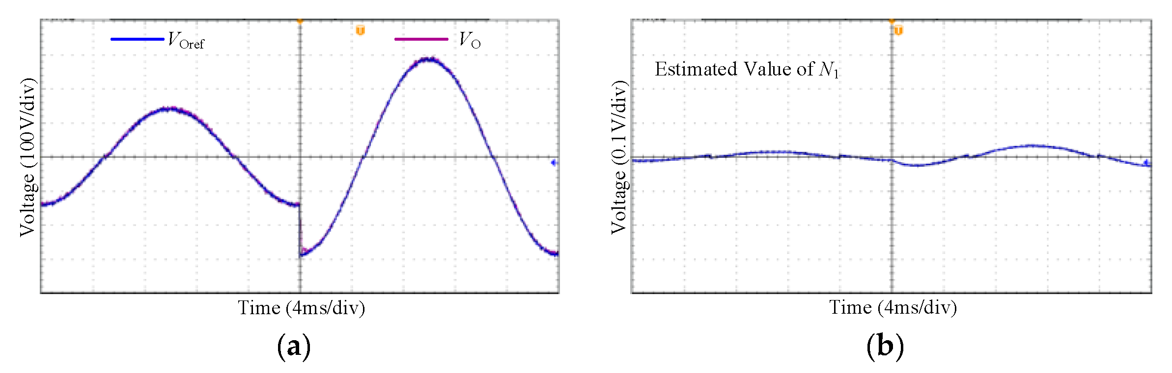
5.2. Dynamic Performance
In order to study the dynamic performance of the proposed RM-MPC, the output voltage reference
Voref is set to a sine wave with an 50 Hz frequency and a 100V RMS value for initialization. However, the RMS value of the desired sine wave steps to 200 V at
t = 0.05 s. And the load is still set to a 20 Ω resistor. The experiment results are shown in
Figure 6, where (a) shows the waveforms of
Vo and its reference
Voref, (b) shows the waveform of the estimated value of
N1, (c) shows the waveform of the estimated value of
N2, (d) shows the waveforms of the two capacitor voltages in the dc side.
It can be seen that the output voltage tracks the step variation of its reference quickly, and the tracking error is reduced to 1 V within 0.54 ms. Besides, the two capacitor voltages in the dc side are also well balanced during transient variation. Thus, the fast dynamic performance of the proposed multilayer MPC is verified. Moreover,
Figure 6b,c shows that the estimated values of
N1 and
N2 change quickly with the step variation of
Voref, so that the fast dynamic performance of the designed Luenberger observer is also verified.
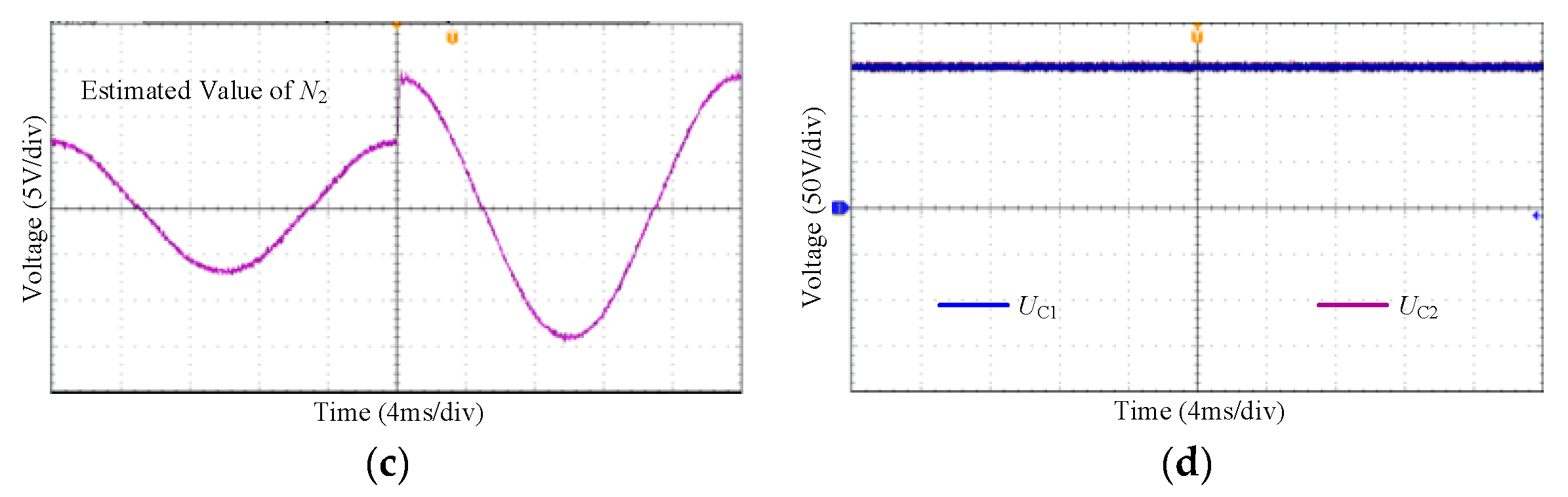
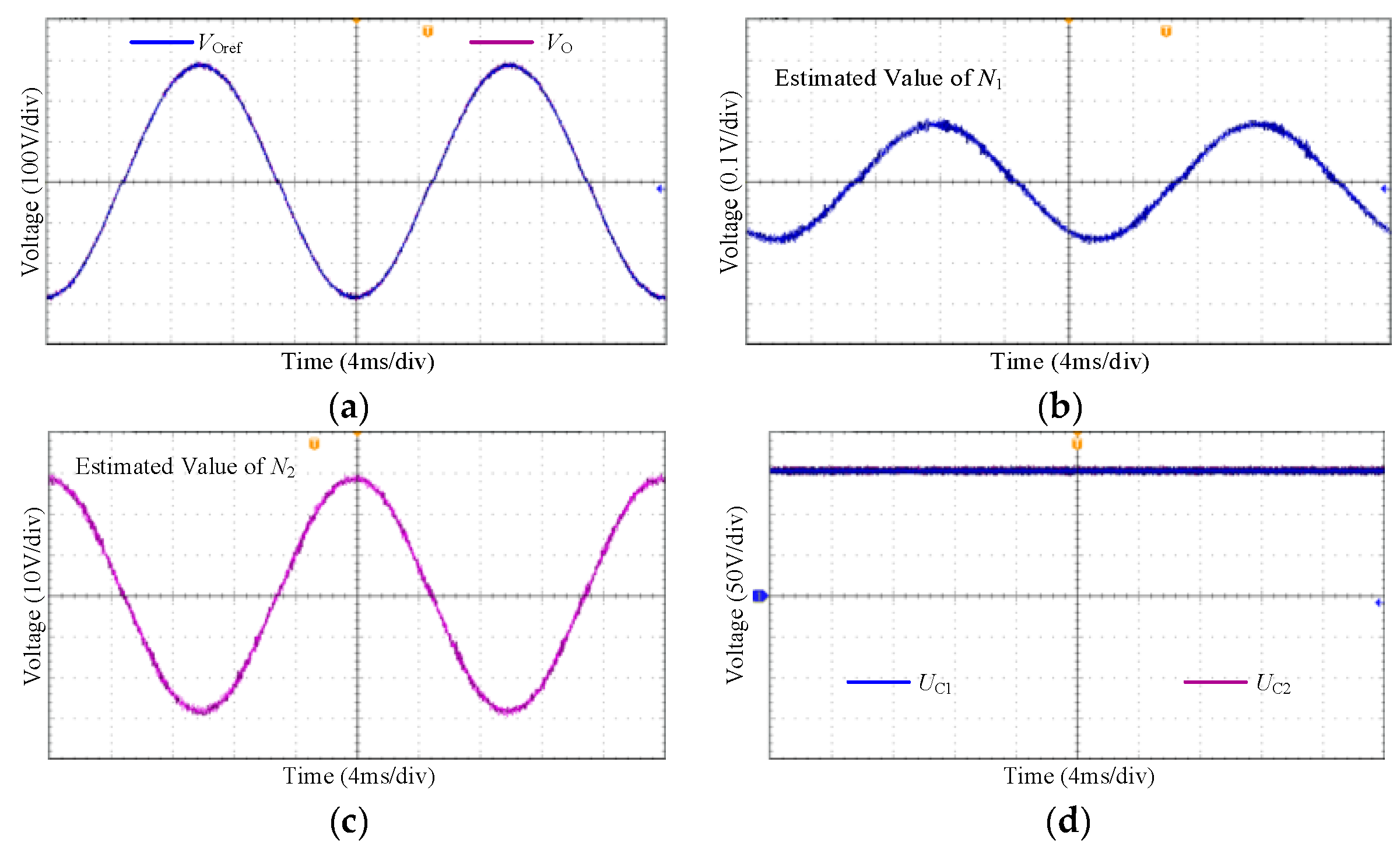
5.3. Robust Performance
In order to study the robust performance of the proposed RM-MPC, two groups of experiments are carried out, where the output voltage reference Voref is set to a sine wave with an 50 Hz frequency and a 200 V RMS value, and the load is also set to a 20 Ω resistor. However, in the first group, the inductance value used in the controller is set to 1 mH, and the capacitance value used in the controller is set to 5 uF, which means that there are −50% parameter mismatch. In the second group, the inductance value used in the controller is set to 3 mH, and the capacitance value used in the controller is set to 15 uF, which means that there are +50% parameter mismatch.
The results of the first group experiment are shown in
Figure 7, where (a) shows the waveforms of
Vo and its reference
Voref, (b) shows the waveform of the estimated value of
N1, (c) shows the waveform of the estimated value of
N2, (d) shows the waveforms of the two capacitor voltages in the dc side. And the results of the second group experiment are shown in
Figure 8.
It can be seen that the good tracking effect of the output voltage are maintained with the help of the designed Luenberger observer, even if there are ±50% parameter mismatches. Furthermore, the well capacitor voltage balancing is also achieved against the parameter mismatches. Thus the strong robustness is also verified by the experiment results.


