Article

A 270-GHz Push-Push Transformer-Based Oscillator Adopting Power Leakage Suppression Technique

1
School of Electrical Engineering, Korea Advanced Institute of Science and Technology, Daejeon 34141, Korea
2
School of Electrical Engineering, Chungbuk National University, Cheongju 28644, Korea
*
Author to whom correspondence should be addressed.
Electronics 2019, 8(11), 1347; https://doi.org/10.3390/electronics8111347
Submission received: 30 October 2019 / Revised: 9 November 2019 / Accepted: 11 November 2019 / Published: 14 November 2019
(This article belongs to the Special Issue Smart Electrical Circuits and Systems for Neural Interface)

Abstract

:
A push–push transformer-based oscillator (TBO) adopting a power leakage suppression technique has been proposed. The proposed technique reduces the power loss due to unwanted leakage path without additional DC power consumption, hence improving the output power and DC-to-RF efficiency. The measured output power of the proposed single core oscillator is −4.5 dBm at 270 GHz with 2.1% DC-to-RF efficiency.

1. Introduction

Recently, terahertz (THz) technologies have been actively studied because of their potential for various applications. The characteristic of THz signal to be able to penetrate non-conducting material allows enclosed object imaging [1,2], which makes it suitable for security application [3,4]. THz imaging also emerges as a new feasible medical modality for a wide range of biomedical applications from dentistry, dermatology and oncology to neurology and physiology [5,6,7,8,9,10,11]. High absorption characteristic of THz signal into water can also be utilized to detect the water content of an object [12,13]. Many different types of toxic gas molecules exhibit vibrational resonance at frequencies between 200 and 300 GHz [14,15]. THz signals can be used for material (gas) ingredient identifications and concentration measurement [16,17,18,19]. THz radiation is also utilized for near-field imaging application which produces high-resolution images [20]. Recently, a fully integrated 550 GHz near-field sensor is also reported with lateral resolution of 8 μ m [21]. Even though with all these potential applications, one big obstacle for THz technology is the lack of compact signal source with high output power and high DC-to-RF efficiency.
Compound semiconductor technology is one of the candidate technologies for THz source development due to its high maximum oscillation frequency ( f m a x ) property. Gunn Diodes based THz oscillator have been reported in [22,23,24,25]. However, these oscillators are only capable to generate output power less than −9 dBm with lower than 0.05% of DC-to-RF efficiency. Performance improvement is achieved by the Resonant Tunnelling Diodes (RTD) based THz oscillators reported in [26,27,28,29,30], which are able to generate up to 0 dBm of output power. Even so, the DC-to-RF efficiency of the reported RTD based THz oscillators are still less than 0.6%.
Silicon technology such as CMOS is also considered as an attractive technology for THz applications due to its advantage in cost and high level integration. Despite of the scaling-down trend of the CMOS technology, the f m a x of CMOS transistor is still below 400 GHz [31]. Moreover, the passive metal structures implemented in CMOS technologies suffer from high loss. Due to these drawbacks, the reported oscillators with fundamental frequency over 200 GHz tend to generate low output power with poor DC-to-RF efficiency. In [31], adopting a cross-coupled oscillator topology, a 210 GHz fundamental frequency oscillator fabricated in 32-nm CMOS is able to generate only −13.5 dBm of output power with 0.11% of DC-to-RF efficiency. Two fundamental frequency oscillators adopting a differential colpitts oscillator topology are also reported in [32]. Fabricated in 32-nm CMOS, the 240 and 272 GHz oscillators are able to generate only −7 and −22 dBm of maximum output power with 1.0% and 0.1% of DC-to-RF efficiency, respectively. The output power of these oscillators are much lower than that of the majority of the reported oscillators, operating above 200 GHz, which generally adopt a push–push oscillator.
Instead of extracting the power at fundamental frequency ( f o ), the push–push oscillator extracts power at the 2nd harmonic frequency ( 2 f o ) which is generated by the non-linear behaviour of the transistor. Several single and multiple-core push–push oscillators have been reported [33,34,35,36,37]. In [33], a single core push–push oscillator adopting differential colpitts topology is reported. Fabricated in 130-nm SiGe, the reported 212 GHz oscillator is able to achieve maximum output power of −7.1 dBm with 0.65% of DC-to-RF efficiency. Combining the output power from several oscillator cores becomes one of the options to further increase the output power of a push–push oscillator. The work in [35] reports a push–push oscillator that combines the output power from 8 oscillator cores. The work in [35] also proposes a push–push oscillator topology called a self-feeding oscillator with capacitive degeneration which can improve the 2nd harmonic power generation from a transistor. Fabricated in 65-nm CMOS, the reported 256 GHz oscillator is able to generate 4.1 dBm of total output power with 1.13% of DC-to-RF efficiency. Finally, a push–push oscillator topology called a transformer-based oscillator is proposed in [37], which can efficiently extract the 2nd harmonic power from a transistor. Fabricated in 65-nm CMOS, the reported 239 GHz oscillator is able to generate −4.8 dBm of output power with 1.47% of DC-to-RF efficiency. Even though the previously reported push–push oscillators in [33,34,35,36,37] show better performance than the previously reported fundamental oscillators in [31,32], the reported DC-to-RF efficiency is still less than 1.5%. Moreover, each oscillator core reported in [33,34,35,36,37] is unable to generate an output power of more than −4.8 dBm. Therefore the output power and DC-to-RF efficiency of push–push oscillators are the areas that require improvement for the development of THz signal sources. One of the problems in push–push oscillators is the configuration of its passive components may introduce an unwanted power leakage path, which can degrade the overall power of THz oscillator.
In this work, a power leakage path is identified from a push–push transformer-based oscillator (TBO) topology [37]. A technique is proposed that can increase the overall power delivered to the output terminal without requiring additional DC power consumption, which leads to the improvement in DC-to-RF efficiency of the proposed oscillator, which is explained in Section 2, including theoretical analysis regarding the effect of Center-Tap (CT) impedance on the push–push TBO output power. The detailed implementation and measurement results of the proposed oscillator are explained in Section 3. Finally, some concluding remarks are given in Section 4.

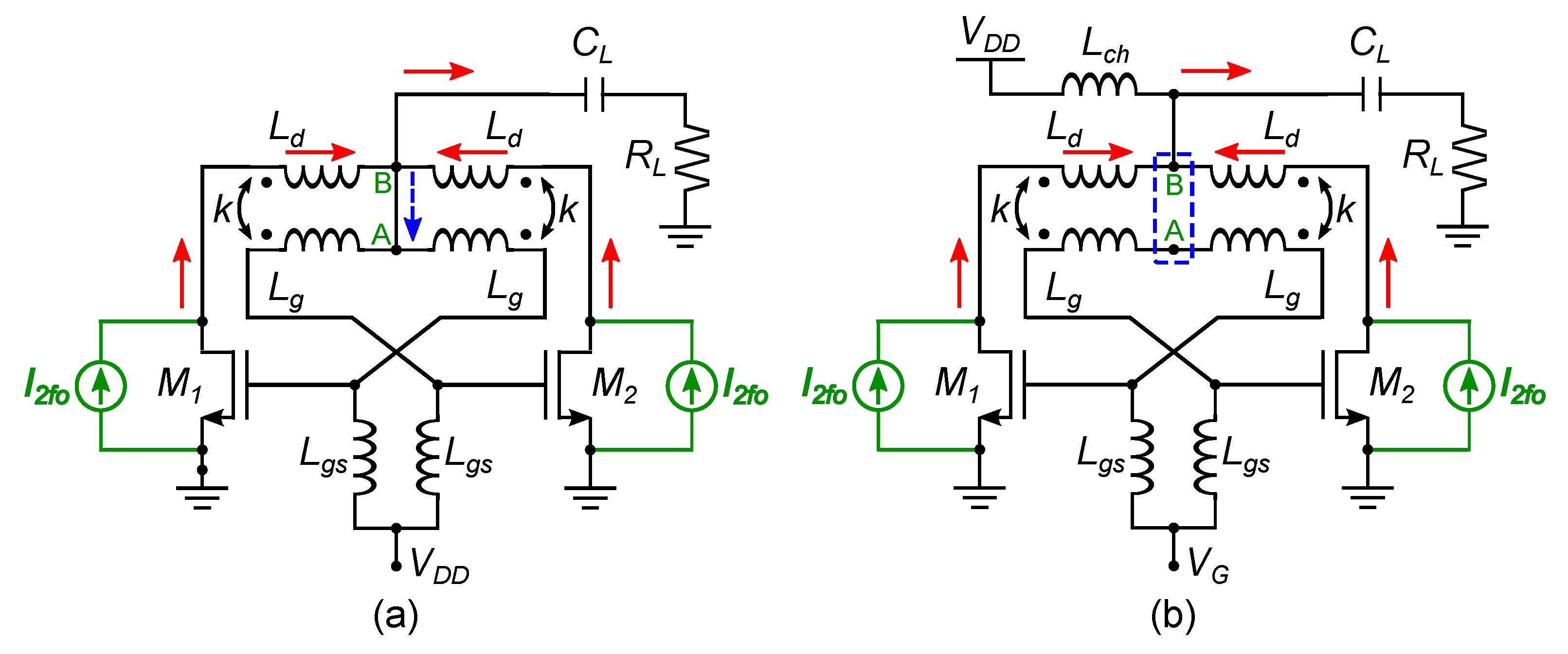
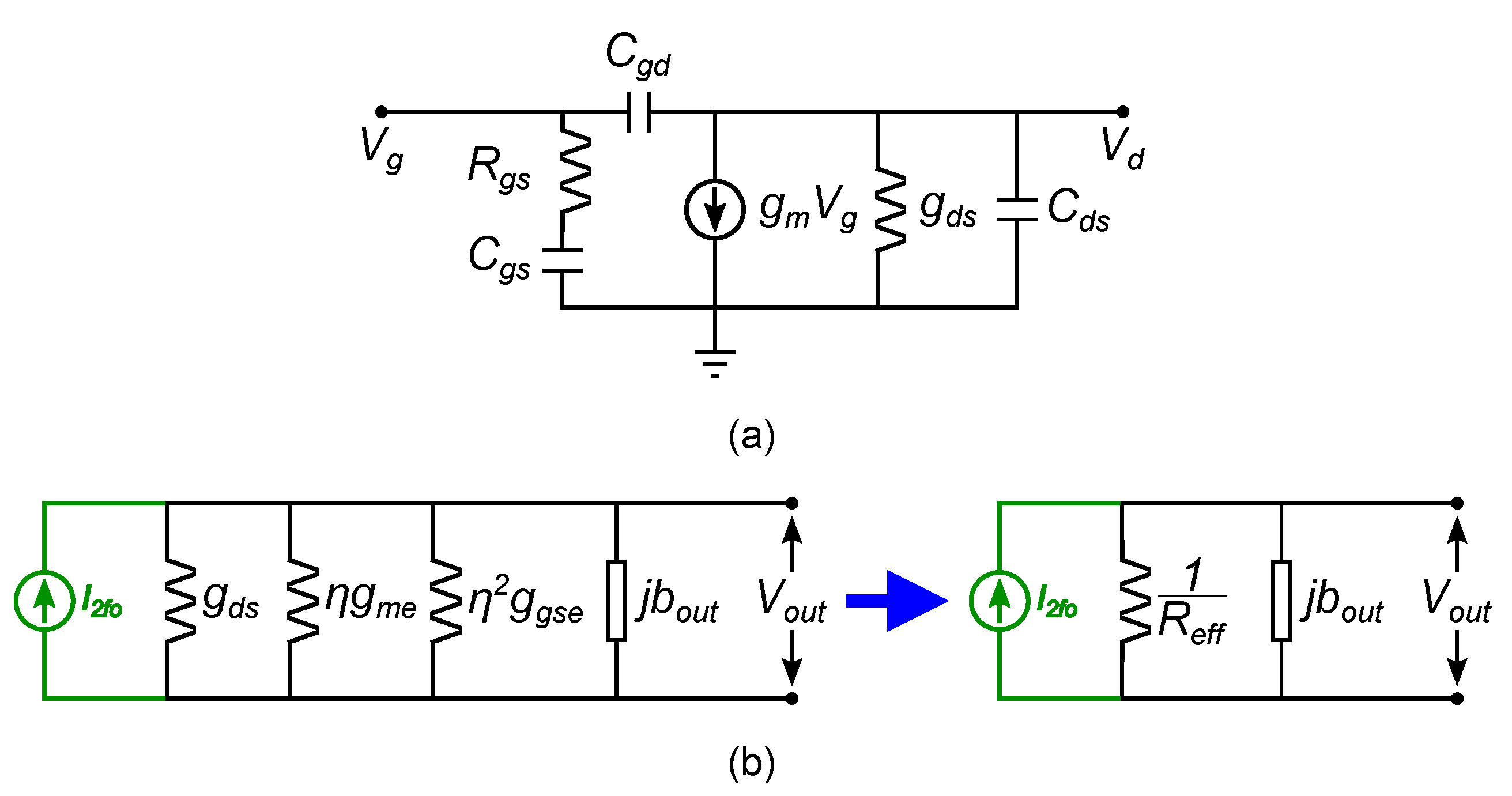
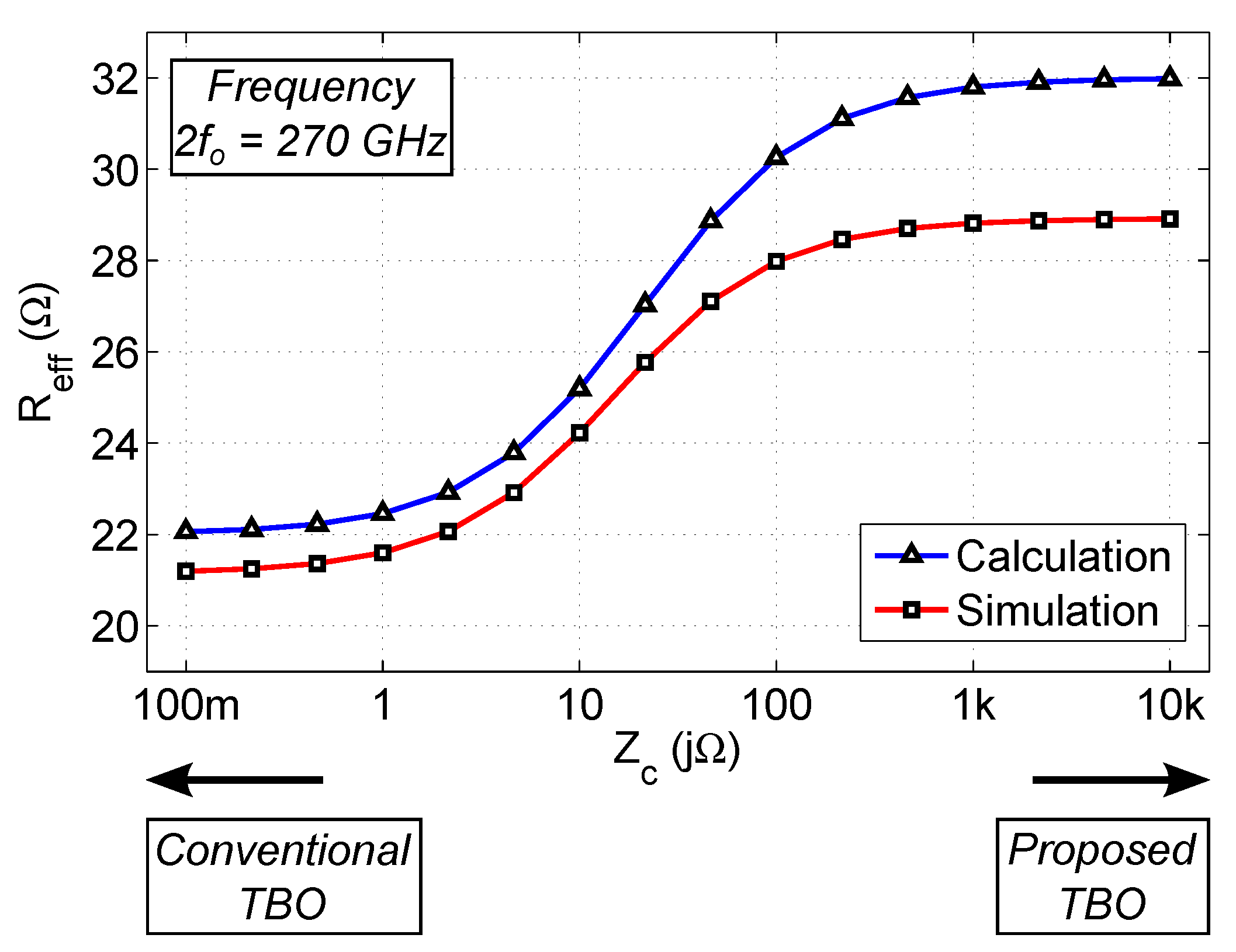
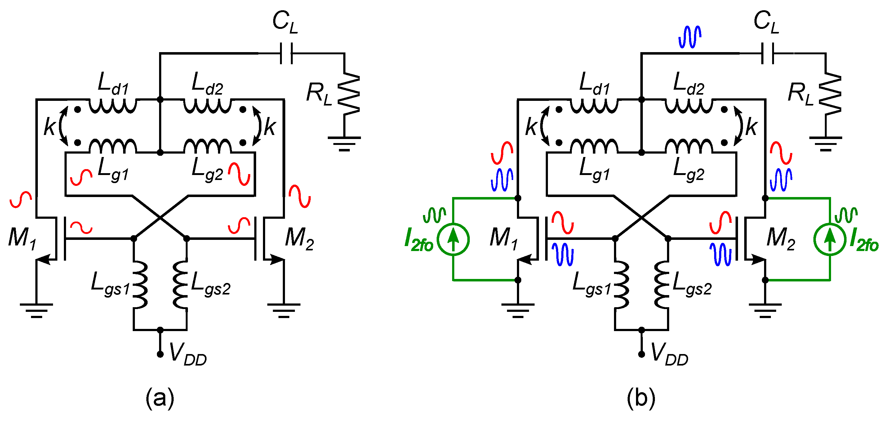
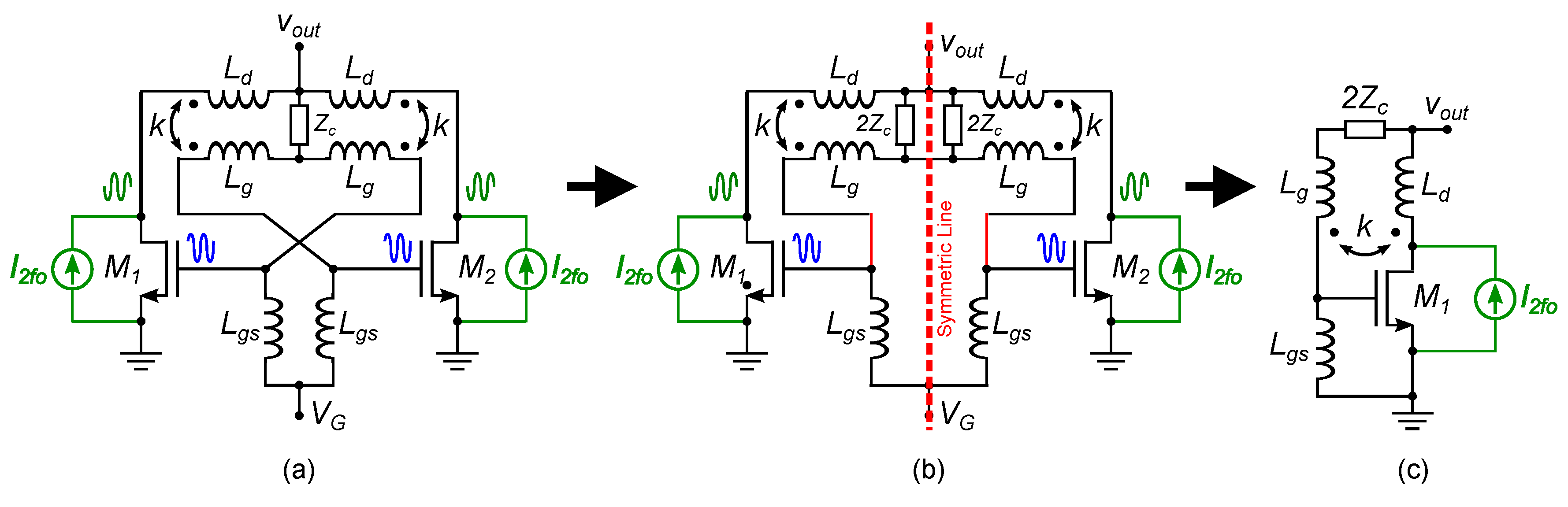
2. Push-Push Transformer-Based Oscillator Operation and the Proposed Oscillator Topology

The works in [33,34,35,36,37] reported several push–push oscillator topologies such as push–push colpitts, self-feeding and transformer-based oscillator. Comparing the measured performance of the oscillators reported in [33,34,35,36,37], the push–push TBO in [37] demonstrates the best performance in terms of output power per single oscillator core and DC-to-RF efficiency.
Figure 1 shows the schematic of the conventional push–push TBO reported in [37]. The operation of a push–push TBO can be described as follow. At the resonant frequency f o , transistors M 1 and M 2 provide an amplification while also providing a 180 phase shift. As shown in Figure 1a, the f o signal at the gate of M 1 is amplified, while its phase is also shifted by 180 . The resulting f o signal is then induced to the secondary coil ( L g 1 ) of the transformer. Further amplification and 180 phase shifting process of the f o signal are then provided by M 2 . Finally, the f o signal is then induced to the secondary coil ( L g 2 ) of the transformer. As shown in Figure 1a, the induced signal at L g 2 has the same phase as the signal at the gate of M 1 , however it has larger amplitude. The f o signal will then experience the same process repeatedly so that its amplitude grows larger and larger until the oscillator reaches its saturation condition. As the result, at the steady-state condition, the oscillator is able to maintain the oscillation with an oscillation frequency of f o as shown in Figure 1b.
During its steady-state condition, as shown in Figure 1b, the signals at the drain terminal of M 1 and M 2 have the same amplitude, and so do the signals at the gate terminal of M 1 and M 2 . However, as shown in Figure 1b, the signals at the gate terminal of M 1 and M 2 are out-of-phase (have a 180 phase difference), and so do the signals at the gate terminal of M 1 and M 2 . Due to the non-linear characteristic of the transistors ( M 1 and M 2 ), the drain current components at harmonic frequencies of f o are generated, including the one at 2 f o (2nd harmonic frequency) which is modelled by ideal current sources I 2 f o in Figure 1b. As the f o signals of M 1 and M 2 have 180 phase difference, the phase of I 2 f o generated by M 1 and M 2 are the same (in-phase). As the result, the 2 f o signals at the drain terminal of M 1 and M 2 are also in-phase, and so do the 2 f o signals at the gate terminal of M 1 and M 2 . Finally, a portion of the I 2 f o generated by M 1 and M 2 will then flow to the output terminal and then dissipated by the load R L . The output power of a push–push TBO is determined by how much portion of I 2 f o is delivered to the output terminal. The larger the portion of I 2 f o delivered to the output terminal leads to higher output power. However, as will be explained later, the conventional push–push TBO reported in [37] suffers from an unwanted power leakage path, which reduces the portion of I 2 f o delivered to the output terminal, and degrades the overall push–push TBO output power. Therefore, a design technique to suppress the power leakage in a push–push TBO is needed so that its output power can be improved.
Figure 2 shows the conventional [37] and proposed push–push TBO. In the proposed push–push TBO shown in Figure 2b, the center-tap (CT) nodes between the primary and secondary ports (node A and B) are left unconnected, whereas those of the conventional push–push TBO are connected, as shown in Figure 2a. Owing to the differential mode operation at the fundamental frequency ( f o ), the nodes A and B of both oscillators act as a virtual ground. As a result, when M 1 , M 2 , L d , L g , k and L g s of both oscillators are identical, the operating conditions for the negative conductance and the oscillation frequency at f o are identical. However, for the common-mode operation at the 2nd harmonic frequency ( 2 f o ), the operating mechanism is different.
In Figure 2, the power at 2 f o is generated by M 1 and M 2 , and it is transferred to the load R L through the inductor L d . In the conventional push–push TBO shown in Figure 2a, node A is connected to B at 2 f o , and through this path, the 2 f o power flowing out from the drain terminals of M 1 and M 2 is leaked to the gate terminals of M 1 and M 2 . As a result, the overall oscillator output power is degraded because not all of the 2 f o power from the drain terminals of M 1 and M 2 can be delivered to R L . In contrast to the conventional push–push TBO, in the proposed push–push TBO, node A and B are disconnected. As a result, to the common-mode 2 f o current coming from M 1 and M 2 , the secondary port of the transformer presents an open condition. Therefore, there is no current flow through L g . Thereby, the magnetic coupling between L d and L g at 2 f o is also terminated, such that the gate terminals are completely isolated from the drain terminals, eliminating the 2 f o power leakage path to the gate terminals of M 1 and M 2 and improving the output power of proposed push–push TBO.
For the better understanding, Figure 3 shows a general model of push–push TBO that includes the CT impedance Z c , and its transformation into equivalent half-circuit at 2 f o . In Figure 3, Z c is connected between CT nodes of primary and secondary inductors of L d and L g . As shown in Figure 3a, the 2 f o signals at the drain terminal of M 1 and M 2 are in-phase (have the same phase), and so do the 2 f o signals at the gate terminal of M 1 and M 2 . As the result, the general model shown in Figure 3a can be simplified into the equivalent circuit model shown in Figure 3b. Finally, making use of the symmetric property in a push–push TBO, an equivalent half-circuit model shown in Figure 3c is used to simplify the analysis of push–push TBO behaviour at 2 f o operation.
Let us assume that the transformer is lossless. Figure 4 shows the equivalent circuit for the MOSFET and the push–push TBO at 2 f o . In Figure 4b, where the non-quasi static MOSFET model [38] is adopted, the model parameters are given by
η = | Z d | | Z g + 2 Z c |
g m e g m ( ω C d s + b 1 ) ( b g s + b 2 ) g d s g g s g g s 2 + ( b g s + b f ) 2
g g s e g g s g d s 2 + ( ω C d s + b 1 ) 2 g g s 2 + ( b g s + b 2 ) 2
where Z g , Z d , g g s , b g s , b o and b f are defined as
Z g = j ω ( L g k L g L d ) Z d = j ω ( L d k L g L d )
g g s = R g s R g s 2 + 1 / ( ω C g s ) 2 b g s = 1 / ( ω C g s ) R g s 2 + 1 / ( ω C g s ) 2
b 1 = I m 1 + j ω C g d Z d + Z g + 2 Z c Z d
b 2 = I m 1 + j ω C g d Z d + Z g + 2 Z c Z g + 2 Z c
assuming b g s 1 / ( ω L g s ) . In Figure 4b, b o u t is the equivalent output susceptance of push–push TBO. From Figure 4b, and assuming that the push–push TBO output is perfectly matched, the total output power of the push–push TBO is given by
P o u t = I 2 f o 2 2 1 g d s + η g m e + η 2 g g s e = I 2 f o 2 2 R e f f
R e f f = 1 g d s + η g m e + η 2 g g s e .
From (8), the output power of the push–push TBO depends on the generated 2nd harmonic current ( I 2 f o ) and the effective resistance ( R e f f ). Higher I 2 f o and R e f f leads to the higher output power.
In Figure 4, the generated 2nd harmonic current ( I 2 f o ) is mainly related to the operation at fundamental frequency ( f o ), especially the voltage swing at drain ( v d , f o ) and gate ( v g , f o ) terminals of the transistor. Figure 5 shows the simulated behaviours of v d , f o , v g , f o and I 2 f o as a function of CT impedance ( Z c ) from the push–push TBO shown in Figure 3. In Figure 3, due to the differential-mode operation of the TBO at the fundamental frequency f o , the CT impedance Z c has no effect on v d , f o , v g , f o , and therefore I 2 f o as well as can be seen in Figure 5. However, unlike I 2 f o , R e f f is affected by Z c as shown in (9), and so does the output power. From (9), the effect of g d s on R e f f is independent of η , whereas g m e and g g s e are dependent on η . From (1), since η has an inversely proportional dependence on Z c , higher Z c leads to increase in R e f f . Therefore, the higher Z c leads to the higher output power in the push–push TBO shown in Figure 3a.
Figure 6 shows the simulated and calculated values of R e f f as a function of Z c . The calculated result is obtained from (8) for the design parameters shown in Table 1 with the small-signal parameters of the transistor extracted from the circuit simulator (Cadence Virtuoso). As can be seen in Figure 6, the calculated R e f f agrees well with the simulation result. In Figure 6 from the simulation result, R e f f increases by 40% when Z c increases from 0.1 Ω to 10 k Ω , indicating the corresponding amount of increase in output power of proposed push–push TBO in comparison with conventional push–push TBO.
Figure 7 shows the CT impedance ( Z c ) as a function of frequency for the proposed and conventional TBOs shown in Figure 1, and Figure 8 shows the corresponding output powers and DC-to-RF efficiencies as a function of the supply voltage ( V D D = V G ) at 270 GHz. Figure 7 and Figure 8 are obtained from the circuit simulator with design parameters shown in Table 1. In Figure 7, the finite values of Z c (∼266 Ω ) in the proposed TBO is induced by the unwanted capacitive coupling between the primary and secondary coils of the transformer. Nonetheless, Z c = 266 Ω helps to suppress the power leakage which leads to approximately 1 dB to 1.5 dB higher output power while achieving 0.3 to 0.6% higher DC-to-RF efficiency compared to those of the conventional push–push TBO (Figure 8).

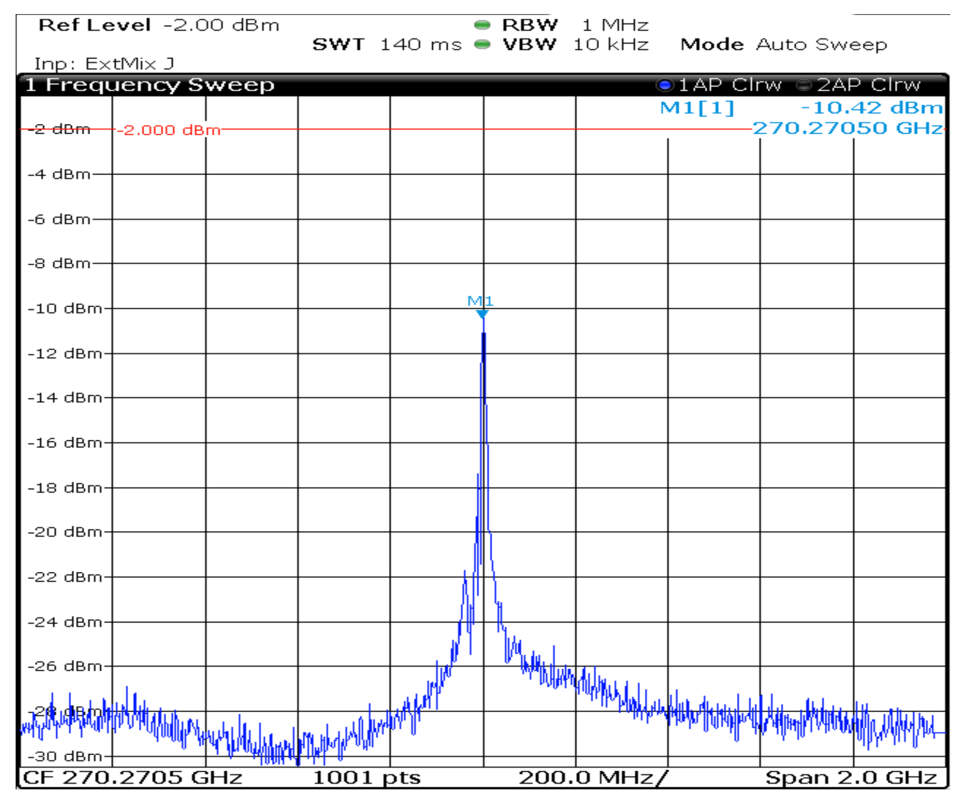
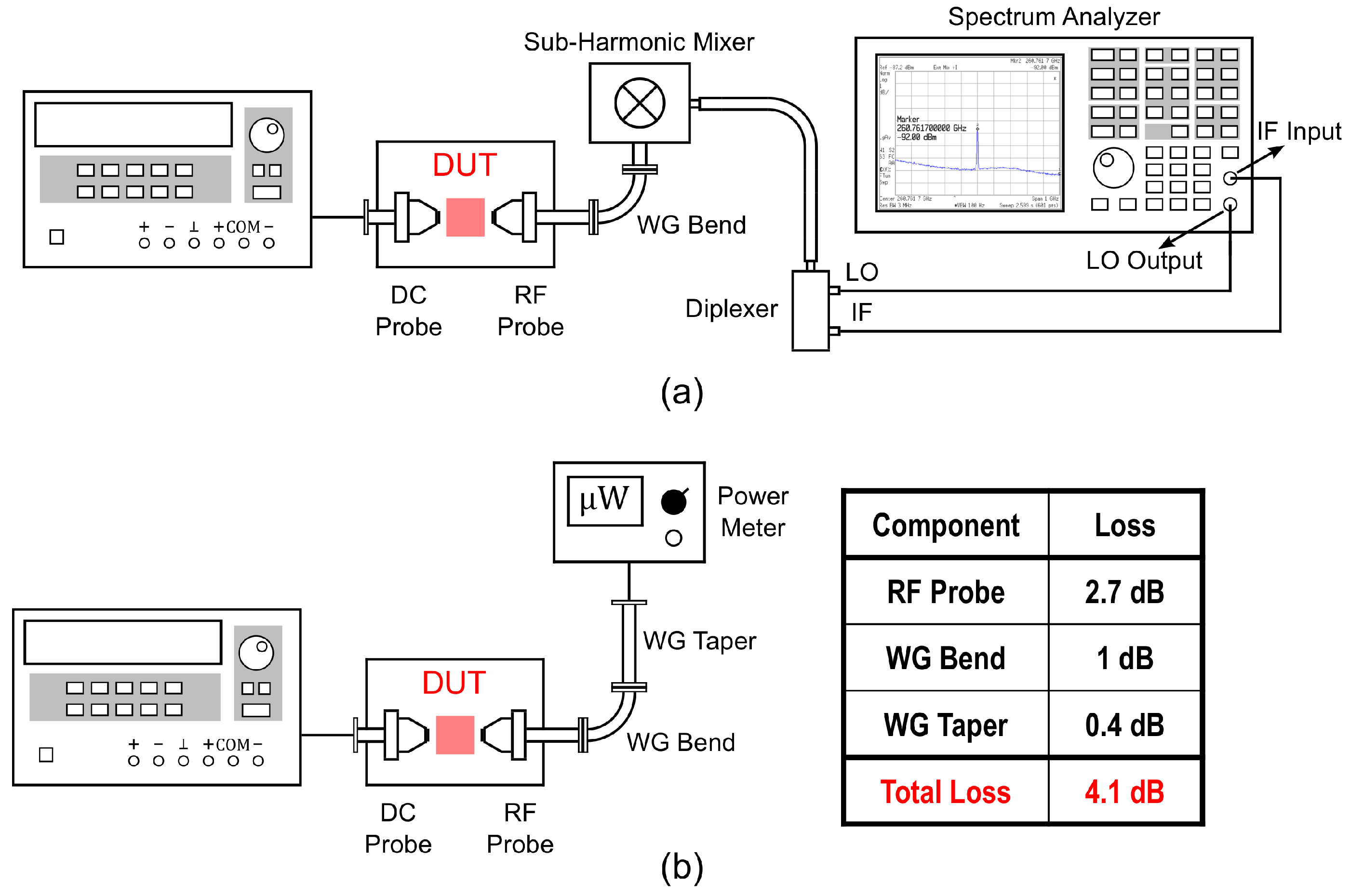
3. Oscillator Implementation and Measurement

As a verification of the proposed power leakage suppression technique, a proposed TBO shown in Figure 2b is implemented in a 65-nm CMOS technology with 2 f o being 240 GHz. The transformers L d and L g are implemented using the top aluminium (Al) layer (metal 10), whereas inductors L g s are implemented using the ultra-thick metal layer (metal 9). The chip photograph of the proposed oscillator is shown in Figure 9, which occupies a total area of 0.46 × 0.20 mm 2 including bias and output pads. Figure 10 shows the experimental setup to measure the output frequency spectrum and output power of the proposed oscillator. For the frequency spectrum measurement, a M03HWD sub-harmonic mixer (conversion loss ∼75 dB), which down converts the TBO output signal to the GHz range of IF frequency, is used as a frequency extension kit of R&S FSW26 spectrum analyzer. For accurate power measurements, the TBO output power is measured using a PM5 power meter. The total power loss of the output power measurement setup is 4.1 dB, which consists of the power losses coming from the RF probe (2.7 dB), waveguide (WG) bend (1 dB) and waveguide taper (0.4 dB).
Figure 11 shows the output frequency spectrum measured at 1.0 V and 1.2 V of V G and V D D , respectively. Over the V G range of 0.7 V to 1.0 V, the measured output frequency varies from 269 GHz to 275 GHz. Due to high conversion loss of the sub-harmonic mixer, the IF signal power is too low to measure the phase noise. Figure 12 shows the measured output power and DC-to-RF efficiency as a function of V D D for V G = 0.8 V, 0.9 V and 1.0 V. Over the ranges of V G and V D D variation, the measured output and DC power vary from −13.1 to −4.5 dBm and 5.8 mW to 17.3 mW, respectively. The proposed oscillator generates the maximum output power of −4.5 dBm at V G = 1.0 V while drawing 14.4 mA of DC current from V D D = 1.2 V, which corresponds to the DC-to-RF efficiency of 2.1%. Compared to the conventional push–push TBO reported in [37], the proposed oscillator achieves 0.3 dB higher output power while consuming 20% lower DC power, hence improving the DC-to-RF efficiency by more than 0.6%.
Due to model inaccuracy of the active and passive components for the operating frequency above 100 GHz, the proposed oscillator operates at around 30 GHz higher than that of the conventional TBO reported in [37]. Moreover, the proposed oscillator consumes less than 20% less DC power compared to the conventional TBO reported in [37]. Therefore, the measured output power of the proposed oscillator (which has 2 f o = 270 GHz) seems to have only 0.3 dB higher than that of the conventional TBO (which has 2 f o = 239 GHz). However, the proposed oscillator is expected to have ∼1 dB higher output power when its DC power consumption is increased from 17.3 mW to 22 mW, which is the same DC power consumed by the conventional TBO in [37]. Moreover, the simulation result in Figure 13 shows that the 30 GHz difference in operating frequency causes ∼0.5 dB difference in the simulated output power of the proposed oscillator. Therefore, the proposed oscillator is expected to achieve ∼1.5 dB improvement of output power compared to the conventional TBO at the same DC power and operating frequency, which is well match with the simulation results of Figure 8.
Table 2 summarizes the performance of the proposed oscillator in comparison with other state-of-the-art oscillators at comparable frequencies. The proposed oscillator shows the best performance in terms of output power and DC-to-RF efficiency which are implemented in the same technology, while operating at higher frequency.

4. Conclusions

This paper analyzed and identified power leakage in a push–push TBO, and proposed a solution to reduce the power loss by the unwanted leakage path without requiring additional DC power consumption. By adopting the proposed technique, the TBO generates higher power than the conventional push–push TBO reported in [37] while operating at 30 GHz higher frequency, and consuming lower DC power, hence achieving higher DC-to-RF efficiency. Implemented in 65-nm CMOS, the measured results of the proposed single core TBO shows an output power of −4.5 dBm at 270 GHz with 2.1% DC-to-RF efficiency. The implemented TBO thus verifies the effectiveness of the proposed power leakage suppression technique to improve the output power and DC-to-RF efficiency.

Author Contributions

Conceptualization, D.R.U. and J.-P.H.; methodology, D.R.U. and J.-P.H.; validation, D.R.U. and D.-W.P.; formal analysis, D.R.U.; investigation, D.R.U.; resources, J.-P.H.; data curation, D.R.U. and D.-W.P.; writing—original draft preparation, D.R.U.; writing—review and editing, J.-P.H., S.-G.L., and D.-W.P.; visualization, D.R.U.; supervision, J.-P.H. and S.-G.L.; project administration, D.-W.P.; funding acquisition, S.-G.L.

Funding

This work was supported by Institute of Information & communications Technology Planning & Evaluation (IITP) grant funded by the Korea government (MSIT) (No. 2019-0-00060).

Conflicts of Interest

The authors declare no conflicts of interest.

References

  1. Ojefors, E.; Pfeiffer, U.R.; Lisauskas, A.; Roskos, H.G. A 0.65 THz Focal-Plane Array in a Quarter-Micron CMOS Process Technology. IEEE J. Solid-State Circuits 2009, 44, 1968–1976. [Google Scholar] [CrossRef]
  2. Al Hadi, R.; Grzyb, J.; Heinemann, B.; Pfeiffer, U.R. A Terahertz Detector Array in a SiGe HBT Technology. IEEE J. Solid-State Circuits 2013, 48, 2002–2010. [Google Scholar] [CrossRef]
  3. Siegel, P.H. Terahertz Technology. IEEE Trans. Microw. Theory Tech. 2002, 50, 910–928. [Google Scholar] [CrossRef]
  4. Federici, J.F.; Schulkin, B.; Huang, F.; Gary, D.; Barat, R.; Oliveira, F.; Zimdar, D. THz imaging and sensing for security applications—Explosives weapons and drugs. Semicond. Sci. Technol. 2005, 20, 266–280. [Google Scholar] [CrossRef]
  5. Fitzgerald, A.J.; Wallace, V.P.; Jimenez-Linan, M.; Bobrow, L.; Pye, R.J.; Purushotham, A.D.; Arnone, D.D. Terahertz Pulsed Imaging of Human Breast Tumors Radiology. Radiology 2006, 239, 533–540. [Google Scholar] [CrossRef]
  6. Oh, S.J.; Kang, J.; Maeng, I.; Suh, J.S.; Huh, Y.M.; Haam, S.; Son, J.H. Nanoparticle-enabled terahertz imaging for cancer diagnosis. Opt. Express 2009, 17, 3469–3475. [Google Scholar] [CrossRef]
  7. Oh, S.J.; Choi, J.; Maeng, I.; Park, J.Y.; Lee, K.; Huh, Y.M.; Suh, J.S.; Haam, S.; Son, J.H. Molucular Imaging with Terahertz Waves. Opt. Express 2011, 19, 4009–4016. [Google Scholar] [CrossRef]
  8. Crawley, D.A.; Longbottom, C.; Cole, B.E.; Ciesla, C.M.; Arnone, D.; Wallace, V.P.; Pepper, M. Terahertz Pulse Imaging: A Pilot Study of Potential Applications in Dentistry. Caries Res. 2003, 37, 352–359. [Google Scholar] [CrossRef]
  9. Wallace, V.P.; Fitzgerald, A.J.; Shankar, S.; Flanagan, N.; Pye, R.; Cluff, J.; Arnone, D.D. Terahertz pulsed imaging of basal cell carcinoma ex vivo and in vivo. Br. J. Dermatol. 2004, 151, 424–432. [Google Scholar] [CrossRef]
  10. Masson, J.B.; Sauviat, M.P.; Martin, J.L.; Gallot, G. Ionic contrast terahertz near-field imaging of axonal water fluxes. Proc. Natl. Acad. Sci. USA 2006, 13, 4808–4812. [Google Scholar] [CrossRef]
  11. Oh, S.J.; Huh, Y.; Haam, S.; Suh, J.; Son, J. Medical application of THz imaging technique. In Proceedings of the International Conference on Infrared, Millimeter and Terahertz Waves, Millimeter, and Terahertz Waves, Wollongong, Australia, 23–28 September 2012; pp. 1–3. [Google Scholar]
  12. Hu, B.B.; Nuss, M.C. Imaging with Terahertz Waves. Optics Lett. 1995, 20, 1716–1718. [Google Scholar] [CrossRef] [PubMed]
  13. Schuster, F.; Videlier, H.; Dupret, A.; Coquillat, D.; Sakowicz, M.; Rostaing, J.P.; Tchagaspanian, M.; Giffard, B.; Knap, W. A Broadband THz Imager in a Low-Cost CMOS Technology. In Proceedings of the IEEE International Solid-State Circuits Conference, San Francisco, CA, USA, 20–24 February 2011; pp. 42–43. [Google Scholar]
  14. Gopalsami, N.; Raptis, A.C. Millimeter-Wave Radar Sensing of Airborne Chemicals. IEEE Trans. Microw. Theory Tech. 2001, 49, 646–653. [Google Scholar] [CrossRef]
  15. Hansen, H.J. Standoff Detection using Millimeter and sub-Millimeter Wave Spectroscopy. Proc. IEEE. 2007, 95, 1691–1704. [Google Scholar] [CrossRef]
  16. Sharma, N.; Zhang, J.; Zhong, Q.; Choi, W.; McMillan, J.P.; Neese, C.F.; De Lucia, F.C. 85-to-127 GHz CMOS Transmitter for Rotational Spectroscopy. In Proceedings of the IEEE 2014 Custom Integrated Circuits Conference, San Jose, CA, USA, 15–17 September 2014; pp. 1–4. [Google Scholar]
  17. Zhong, Q.; Choi, W.; Miller, C.; Haenderson, R.; Kenneth, K.O. 25.2 A 210-to-305GHz CMOS Receiver for Rotational Spectroscopy. In Proceedings of the IEEE International Solid-State Circuits Conference (ISSCC), San Francisco, CA, USA, 31 January–4 February 2016; pp. 426–427. [Google Scholar]
  18. Wu, X.; Sengupta, K. A 40-to-330GHz Synthesizer-free THz Spectroscope-On-Chip Exploiting Electromagnetic Scattering. In Proceedings of the IEEE International Solid-State Circuits Conference (ISSCC), San Francisco, CA, USA, 31 January–4 February 2016; pp. 428–429. [Google Scholar]
  19. Wang, C.; Han, R. Dual-Terahertz-Comb Spectrometer on CMOS for Rapid, Wide-Range Gas Detection With Absolute Specificity. IEEE J. Solid-State Circuits 2017, 52, 3361–3372. [Google Scholar] [CrossRef]
  20. Adam, A. Review of Near-Field Terahertz Measurement Methods and Their Applications. J. Infrared Millim. Terahertz Waves 2011, 32, 976–1019. [Google Scholar] [CrossRef]
  21. Gryzyb, J.; Heinnemann, B.; Pfeiffer, U.R. A Fully Integrated 0.55 THz Near-Field Sensor with a Lateral Resolution Down to 8 μm in 0.13 μm SiGe BiCMOS. IEEE J. Solid-State Circuits 2016, 51, 3063–3077. [Google Scholar] [CrossRef]
  22. Khalid, A.; Dunn, G.M.; Macpherson, R.F.; Thoms, S.; Macintyre, D.; Li, C.; Steer, M.J.; Papageorgiou, V.; Thayne, I.G.; Kuball, M.; et al. Terahertz oscillations in an In0.53Ga0.47As submicron planar Gunn diode. J. Appl. Phys. 2014, 115, 114502. [Google Scholar] [CrossRef]
  23. Khalid, A.; Li, C.; Papageogiou, V.; Dunn, G.M.; Steer, M.J.; Thayne, I.G.; Kuball, M.; Oxley, C.H.; Montes Bajo, M.; Stephen, A.; et al. In0.53Ga0.47As Planar Gunn Diodes Operating at a Fundamental Frequency of 164 GHz. IEEE Electron Device Lett. 2013, 34, 39–41. [Google Scholar] [CrossRef]
  24. Maricar, M.I.; Glover, J.; Khalid, A.; Li, C.; Evans, G.; Cumming, D.R.S.; Oxley, C.H. An AlGaAs/GaAs-based planar Gunn diode oscillator with a fundamental frequency operation of 120 GHz. IEEE Microw. Opt. Technol. Lett. 2014, 56, 2449–2451. [Google Scholar] [CrossRef]
  25. Khalid, A.; Li, C.; Papageogiou, V.; Pilgrim, N.J.; Dunn, G.M.; Cumming, D.R.S. A 218-GHz second-harmonic multiquantum well GaAs-based planar Gunn diodes. IEEE Microw. Optical Tech. Lett. 2013, 55, 686–688. [Google Scholar] [CrossRef]
  26. Wang, J.; Alharbi, K.; Ofiare, A.; Zhou, H.; Khalid, A.; Cumming, D.; Wasige, E. High Performance Resonant Tunneling Diode Oscillators for THz Applications. In Proceedings of the IEEE Compound Semiconductor Integrated Circuit Symposium (CSICS), New Orleans, LA, USA, 11–14 October 2015; pp. 1–4. [Google Scholar]
  27. Wang, J.; Al-Khalidi, A.; Alharbi, K.; Ofiare, A.; Zhou, H.; Wasige, E.; Figueiredo, J. High Performance Resonant Tunneling Diode Oscillators as Terahertz Sources. In Proceedings of the 46th European Microwave Conference (EuMC), London, UK, 4–6 October 2016; pp. 341–344. [Google Scholar]
  28. Al-Khalidi, A.; Alharbi, K.; Wang, J.; Wasige, E. A Compact Terahertz Source Technology for Automotive Radar and Other Applications. In Proceedings of the 19th International Radar Symposium (IRS), Bonn, Germany, 20–22 June 2018; pp. 1–6. [Google Scholar]
  29. Wasige, E.; Alharbi, K.; Al-Khalidi, A.; Wang, J.; Khalid, A.; Rodrigues, G.C.; Figueiredo, J. Resonant tunnelling diode terahertz sources for broadband wireless communications. In Terahertz, RF, Millimeter, and Submillimeter-Wave Technology and Applications X; SPIE: Bellingham, WA, USA, 2017. [Google Scholar]
  30. Hinata, K.; Shiraishi, M.; Suzuki, S.; Asada, M. High power THz oscillators with offset-fed slot antenna and high current density resonant tunneling diodes. In Proceedings of the 34th International Conference on Infrared, Millimeter, and Terahertz Waves, Busan, Korea, 21–25 September 2009; pp. 1–2. [Google Scholar]
  31. Wang, Z.; Chiang, P.; Nazari, P.; Wang, C.; Chen, Z.; Heydari, P. A CMOS 210-GHz Fundamental Transceiver With OOK Modulation. IEEE J. Solid-State Circuits 2014, 49, 564–580. [Google Scholar] [CrossRef]
  32. Landsberg, N.; Socher, E. 240 GHz and 272 GHz Fundamental VCOs Using 32 nm CMOS Technology. IEEE Trans. Microw. Theory Technol. 2013, 61, 4461–4471. [Google Scholar] [CrossRef]
  33. Chiang, P.Y.; Momeni, O.; Heydari, P. A 200-GHz Inductively Tuned VCO With -7-dBm Output Power in 130-nm SiGe BiCMOS. IEEE Trans. Microw. Theory Technol. 2013, 61, 3666–3673. [Google Scholar] [CrossRef]
  34. Han, R.; Afshari, E. A CMOS High-Power Broadband 260-GHz Radiator Array for Spectroscopy. IEEE J. Solid-State Circuits 2013, 48, 3090–3104. [Google Scholar] [CrossRef]
  35. Adnan, M.; Afshari, E. A 247-to-263.5GHz VCO with 2.6mW peak output power and 1.14% DC-to-RF efficiency in 65 nm Bulk CMOS. In Proceedings of the IEEE International Solid-State Circuits Conference Digest of Technical Papers (ISSCC), San Francisco, CA, USA, 9–13 February 2014; pp. 262–263. [Google Scholar]
  36. Kananizadeh, R.; Momeni, O. A 190-GHz VCO With 20.7% Tuning Range Employing an Active Mode Switching Block in a 130 nm SiGe BiCMOS. IEEE J. Solid-State Circuits 2017, 52, 2094–2104. [Google Scholar] [CrossRef]
  37. Koo, H.J.; Kim, C.Y.; Hong, S.C. Design and Analysis of 239 GHz CMOS Push-Push Transformer-Based VCO With High Efficiency and Wide Tuning Range. IEEE Trans. Circuits Syst. I Regul. Pap. 2015, 62, 1883–1893. [Google Scholar] [CrossRef]
  38. Kordalski, W.J.; Stefanski, T. A non-quasi-static small-signal MOSFET model for radio and microwave frequencies including spreading gate resistances and capacitances. In Proceedings of the IEEE Radio Frequency Integrated Circuits (RFIC) Symposium, Philadelphia, PA, USA, 9–10 June 2003; pp. 365–368. [Google Scholar]
Figure 1. Schematic of conventional push–push TBO (a) small signal operation and (b) steady-state (large signal) operation.
Electronics 08 01347 g001
Figure 2. Schematic of push–push TBO (a) conventional and (b) proposed.
Electronics 08 01347 g002
Figure 3. Push-push TBO (a) general model, (b) simplified model, and (c) equivalent half-circuit at 2 f o .
Electronics 08 01347 g003
Figure 4. Push-push TBO (a) NQS (Non-Quasi Static) MOSFET model and (b) equivalent circuit at 2 f o .
Electronics 08 01347 g004
Figure 5. Simulated v d , f o , v g , f o and I 2 f o as a function of CT impedance ( Z c ).
Electronics 08 01347 g005
Figure 6. Simulated and calculated effective output resistance ( R e f f ) as a function of CT impedance ( Z c ).
Electronics 08 01347 g006
Figure 7. Simulated CT impedance ( Z c ) of conventional and proposed TBOs.
Electronics 08 01347 g007
Figure 8. Simulated output power and DC-to-RF efficiency of conventional and proposed TBOs as a function of V D D = V G .
Electronics 08 01347 g008
Figure 9. Chip photograph of the proposed oscillator ( 0.46 × 0.20 mm 2 ).
Electronics 08 01347 g009
Figure 10. Experimental setup to measure (a) output frequency spectrum, and (b) output power with insertion loss details.
Electronics 08 01347 g010
Figure 11. Measured frequency spectrum of the proposed oscillator with calibrated power level.
Electronics 08 01347 g011
Figure 12. Measured output power and DC-to-RF efficiency of the proposed oscillator.
Electronics 08 01347 g012
Figure 13. Simulated output power of the proposed oscillator at two different output frequencies.
Electronics 08 01347 g013
Table 1. Design Parameters of Proposed Oscillator.
ComponentValueComponentValue
M 1 , M 2 19.2 μ m/60 nm L g 41 pH (Q : 11)
( f m a x )(300 GHz)k0.33
L d 44 pH (Q : 15) L g s 148 pH (Q : 25)
Table 2. Comparison with state-of-the-art oscillators around 250 GHz.
References[37][32][35][36][33][34]This Work
TopologyTransformer BasedColpittsSelf FeedingColpittsColpittsSelf FeedingTransformer Based
f o (GHz)239272256190.5212260270
P out (dBm)−4.8−224.1−2.1−7.10.5−4.5
# of Core1182181
P out /Core (dBm)−4.8−22−4.9−5.1−7.1−8.5−4.5
P DC (mW)227227183/2943080017.3
Efficiency1.47%0.09%1.13%0.22%0.65%0.14%2.10%
Technology65-nm CMOS32-nm CMOS65-nm CMOS130-nm SiGe130-nm SiGe65-nm CMOS65-nm CMOS
MeasurementProbeProbeProbeProbeProbeAntennaProbe

