Review

Review of Multilevel Voltage Source Inverter Topologies and Analysis of Harmonics Distortions in FC-MLI

1
School of Electrical Engineering, Pusan National University, Busandaehak-ro 63 beongil 2, Busan 46241, Korea
2
Department of Electrical Engineering and Electrical Engineering Management, University of technology Sydney, 15 Broadway Ultimo, Sydney, NSW 2007, Australia
*
Authors to whom correspondence should be addressed.
Electronics 2019, 8(11), 1329; https://doi.org/10.3390/electronics8111329
Submission received: 25 September 2019 / Revised: 3 November 2019 / Accepted: 6 November 2019 / Published: 11 November 2019
(This article belongs to the Special Issue Power Converters in Power Electronics)

Abstract

:
We review the most common topology of multi-level inverters. As is known, the conventional inverters are utilized to create an alternating current (AC) source from a direct current (DC) source. The two-level inverter provides various output voltages [(Vdc/2) and (−Vdc/2)] of the load. It is a successive method, but it makes the harmonic distortion of the output side, Electromagnetic interference (EMI), and high dv/dt. We solve this problem by constructing the sinusoidal voltage waveform. This is achieved by a “multilevel inverter” (MLI). The multilevel inverter creates the output voltage with multiple DC voltages as inputs. Many voltage levels are combined to produce a smoother waveform. During the last decade, the multilevel inverter has become very popular in medium and high-power applications with some advantages, such as the reduced power dissipation of switching elements, low harmonics, and low EMIs. We introduce the information about several multilevel inverters such as the diode-clamped multilevel inverter (DC-MLI), cascaded H-bridge multilevel inverter (CHB-MLI), and flying-capacitor multilevel inverter (FC-MLI) with Power systems CAD (PSCAD) simulation. It is shown that THD is 28.88% in three level FC-MLI while THD is 18.56% in five level topology. Therefore, we can decrease the total harmonic distortion adopting the higher-level topology.

1. Introduction

Inverters are very useful for various industrial applications. In the last few years, the voltage-driving method has been adopted. To reduce the semiconductor transient voltage and current rating, a series and parallel connection method is needed. Moreover, the limited standard three-phase converter is also adopted up to the maximum allowable voltage of the load. Also, both the primary and the Pulse width modulation (PWM) switching frequency can be useful. The reduced switching frequency shows the low disappearance and the higher efficiency. In order to synthesize the spectrum signals of the harmonics caused by the capacity, the multi-level inverter has received more attention in recent times. Moreover, a multilevel inverter has a key role in providing improved operating voltage beyond the voltage limits of conventional semiconductors.
The following clarification defines the significance of the multilevel converter. The explanation of a multilevel inverter is: “The multilevel inverter can demonstrate the switching skill very effectively with different voltage and current levels of its input or output nodes”. It is a practical reply to raise the power capacity with a comparably low elements load and decreasing the output harmonics.

The Concept of Multilevel Inverters

Two level inverters are shown in Figure 1. The input voltage of a direct current (DC) is converted to the required alternating current (AC) voltage and frequency [1]. When an inverter operates with Vdc, a two-level inverter can create two different output voltage for a load, Vdc/2 or (−Vdc)/2. To generate an AC voltage, both voltages are generally allowable in the PWM. Compared to multilevel inverters, this two-level method creates harmonic distortion, Electromagnetic interference (EMI), and huge dv/dt [2]. The idea of a multilevel inverter is not based on the two-voltage level AC. Alternatively, some voltage levels are connected to get a better waveform and less dv/dt and harmonic distortion. If the voltage level of the inverter is higher than the waveform, it is much better. However, the designs are simple, but increasing voltage levels and more components are needed. The dividing voltage and extending its control scheme become more complex in a three-phase setup [3]. Series-connected multilevel inverters are connected to the capacitor-composing energy tank of the inverter. That provides many nodes in the inverter connecting to the different phases. The term level does not correspond to the voltage level that can be provided by the output inverter. Diodes can provide the path of reactive source from the load to the power supply at the current and voltage of Resistance Inductor load (RL) load having opposite polarity.
A multilevel inverter has positive points compared with the two-level inverter using the PWM method. Also, a multilevel inverter produces very small distortions and dv/dt in the output side. In addition, it produces a common-mode voltage and operates at a lower switching frequency [2] than a two-stage inverter. Besides, there are several features of a multilevel inverter that can be summarized as the following: (1) the multilevel inverter does not produce low distortion output voltage, but it also decreases the dv/dt stresses. Consequently, problems with electromagnetic compatibility are cleared. (2) The multi-level inverter produces a lower voltage in a common mode; as a result, the motor attached load of the multilevel inverter may be decreased. (3) A multilevel inverter draws a small input current distortion. (4) To obtain more output voltage levels using fewer switching devices, many recently structured multilevel inverters have been presented in this publication [4,5,6,7,8,9,10,11,12,13,14,15,16].
In this paper, various multilevel inverter topologies are presented along with their analysis and comparative assessments. Furthermore, these topologies have been checked with the simulation results using PSCAD software. Then a comparison of different types of multilevel inverter topologies and describe PWM control techniques and we can choose one topology for further implementation and selected from the simulation results derived from the MULTISIM software.

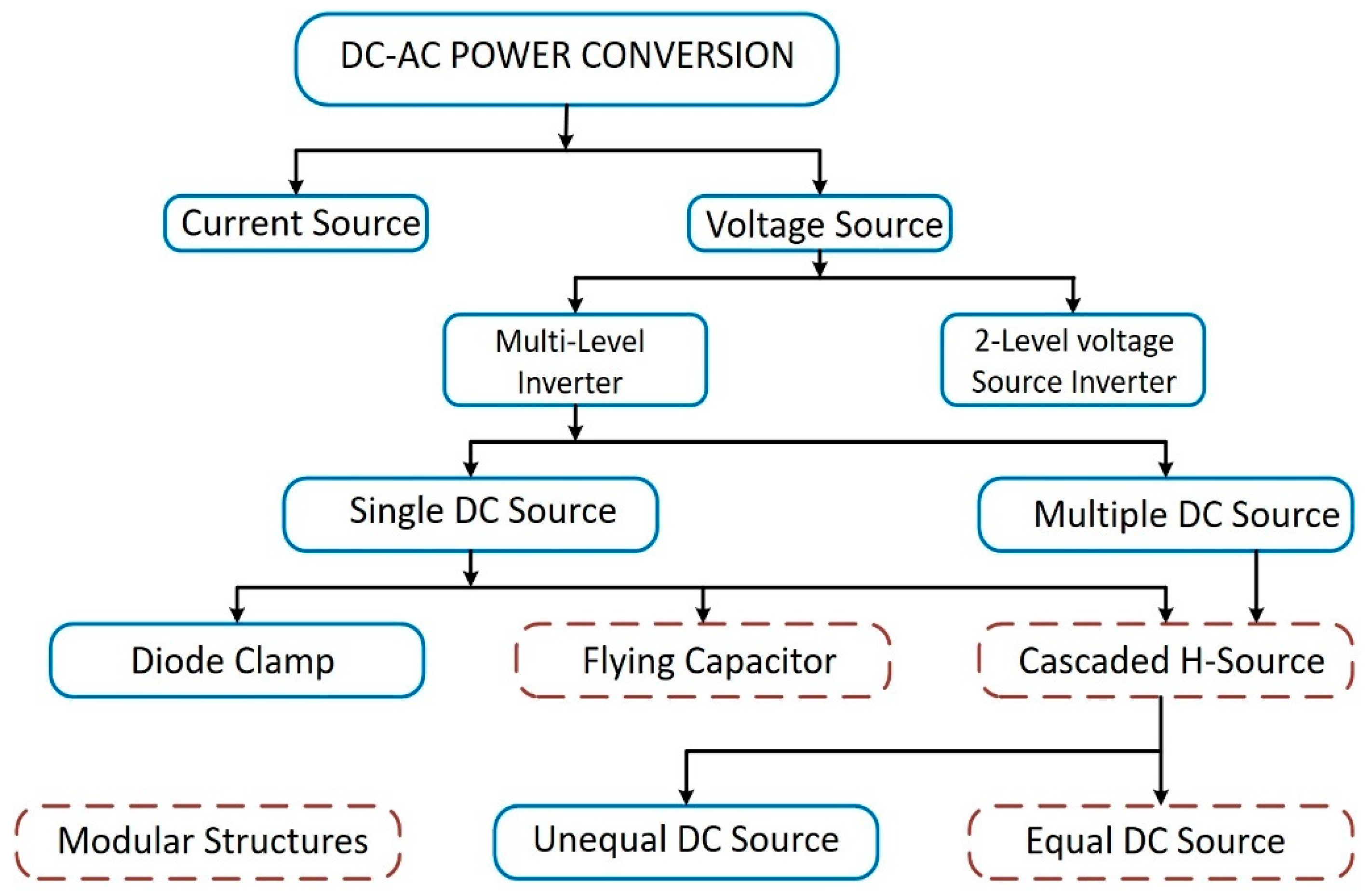
2. Topologies of Multilevel Inverter

Normally, these inverters can be classified as voltage source or current source inverters as shown in Figure 2.
Three major multilevel inverter configurations applied in industrial applications and mentioned in several literatures; cascaded H-bridges inverter with separate DC sources, Diode Clamp, and flying capacitors used virtually in low, medium and high-power applications are briefly discussed.

2.1. Diode-Clamped Multilevel Inverter (DC-MLI)

The multilevel inverter was invented in 1975, which was a cascade diode inverter. After a few years, it was called the diode-clamped multilevel inverter (DC-MLI) [2]. In DC-MLI, voltage clamping diodes are required to regulate the voltage on the DC bus to reach output voltage levels; but the multilevel inverter level should be unique because the neutral point is not available even in number levels [17]. For DC bus with a neutral point and a capacitor, there is a clamping diode attached to the number of valve pairs (m-1), where m is the level of voltage in the inverter. The explanation as to why the frequency converter is connected to the series with a diode; means that all diodes have the same rated voltage and may block a correct voltage level [18].
A 3-level DC-MLI, a voltage per capacitor and switch is Vdc/2. The equations are utilized to decide the number of devices forming a given level of a DC-MLI. If m is the number of levels, the number of capacitors on the DC side (C) can be determined through Equation (1). The number of switches (S) per phase and the clamp diodes (D) can be determined through Equations (2) and (3), respectively. Consequently, 4 switches, 2 diodes, and 2 capacitors are needed as shown in Figure 3a. The intermediate circuit voltage is divided into three phases, with two capacitors C1 and C2 which are attached in series; “n” is a neutral point which is the center point of the capacitors. There are 3 levels of output voltage Vdc/2, 0, (−Vdc)/2, for voltage level Vdc/2, S1 and S2 are activated, for voltage level (−Vdc)/2, S1′ and S2′ are activated, and for 0 level voltage, S2 and S1′ are activated. When S2′ and S1′ are connected, the load is shortened, and the reactive power released.
For the 5-level diode clamped multilevel inverter, m is 5. Following Equations (1), (2) and (3), therefore, 8 switches, 4 diodes, and 4 capacitors are needed. Figure 3b shows that all diodes are designed for Vdc/4, and diodes D1′ block 3Vdc/4. Hence, 3 diodes are connected in a series. At 5 voltage levels, Vdc/2, Vdc/4, 0, (−Vdc)/4, (−Vdc)/2 are five states output. To get various output voltage levels, combinations of switching states are utilized. For Vdc/2, top all switches are activated and, for Vdc/4, S2, S3, S4, and S1′ are activated and a voltage is maintained through a clamping diodes D1 and D1′. For 0 level voltage, S3, S4, S1′ and S2′ are activated, for a voltage (−Vdc)/4, switch S4, S1′, S2′, and S3′ are activated and voltage (−Vdc)/2 the bottom all switches are activated and the diodes D2 and D2′ or D3 and D3′ are maintaining the voltage.
C = m 1
S = 2 ( m 1 )
D = ( m 1 ) ( m 2 )
There are few advantages of DC-MLI: high efficiency, due to the main switching frequency that can be used for all devices. Capacitors are pre-charged as a group; all stages have the usual DC bus. That reduces the capacitance of the inverter. However, there are a few drawbacks of this topology: it is difficult to flow active power, and controlling is quite difficult for the capacitor voltage balance.

2.1.1. 3-Level DC-MLI PSCAD Simulations

In Figure 4a, consider the source voltage as +2 Vdc. There are total two capacitors connected to source, hence the voltage across each capacitor is Vdc. As shown in the switching Table 1 the voltage levels are available as per the switching sequence.
+Vdc: Switches S1, S2 are ON. In this case, current flows from source (charged capacitors C1) to load through switches S1, S2. 0 voltage: Switches S2 and S3 are ON. Hence no capacitor is discharged through the load. Here the load is directly connected to ground at both the ends (shorted). Hence the voltage across the load is 0 V. −Vdc: Switches S3 and S4 are ON. In this case, current flows from source (charged capacitors C2) to the load through switches S3 and S4.
In Figure 4b, a control circuit there is 4 switch signal generated using two comparators. 0–3 V, 50 Hz cycle, a triangular waveform is used for comparison. A different DC signal is used as a base for a comparator. This will generate four signals S1, and S2 with different widths. The other two, S3 and S4, are obtained using NOT gate. These 4 gate signals are ready to supply to IGBT which are in the 3-level DC-MLI power circuit, which is illustrated in Figure 4a.

2.1.2. 5-Level DC-MLI PSCAD Simulations

In Figure 5a, consider the source voltage as +Vdc. There are total four capacitors connected to source, hence the voltage across each capacitor is +Vdc/4. As shown in the switching Table 2 the voltage levels are available as per the switching sequence.
+Vdc/2: Switches S1, S2, S3, S4 are ON. In this case, current flows from source (charged capacitors C1, C2) to load through switches S1, S2, S3, S4. +Vdc/4: Switches S2, S3, S4, and S5 are ON. Here only capacitor C2 discharges through diode D1 and the switches S2, S3, and S4 to the load. Since only half of the capacitor (only C2) discharges, hence total Vdc/4 voltage is available. 0 voltage: Switches S3, S4, S5 and S6 are ON. Hence no capacitor is discharged through the load. Here the load is directly connected to ground at both the ends (shorted). Hence the voltage across the load is 0 V. −Vdc/4: Switches S4, S5, S6, and S7 are ON. Hence the capacitor C3 discharges through the ground–load and switch S5, S6, and S7. As the discharge is in the opposite direction the voltage appeared will be negative. −Vdc/2: Switches S5, S6, S7 and S8 are ON. Capacitor C3 and C4 will discharge through the load in the opposite direction (from the ground to load to switches). Hence total voltage –Vdc/2 will appear across the load. In Figure 5b a control circuit there is 8 switch signal generated using four comparators. 0 – 10 V, 50 Hz cycle, a triangular waveform is used for comparison. And different DC signal is used as a base for a comparator. This will generate four signals S1, S2, S3 and S4 with different widths. Other four S5 to S8 are obtained using NOT gate. These 8 gate signals are ready to supply to IGBT which are in the 5-level DC-MLI power circuit, which is shown in Figure 5a.

2.2. Cascaded H-Bridge Multilevel Inverter (CHB-MLI)

There are various inverter topologies based on a series single-phase inverter connected to the individual DC source. If an inverter is implemented in an active transfer of source applications, then the sources of each bridge must be separated. Due to this property, it is recommended to use a cascaded H-bridge multilevel inverter (CHB-MLI) in fuel cells or photovoltaic (PV) array to reach a higher level [19,20,21].
The resulting phase voltage has been synthesized through increasing the generated voltages through different cells. The module of a bridge is a three-level in CHB-MLI, and each module is appended to the cascade. The output voltage for an n-level cascade multilevel inverter is 2n + 1, where n is the source of DC [22]. Switching angles are obtained to reduce the overall distortion of harmonics. Maximum output voltage is decided by using Equation. (6) and minimum output voltage is decided by using Equation (7). The capacitors at the DC side (C) and several switches (S) per phase, calculated through Equations (4) and (5) respectively.
C = m 1 2  
S = 2 ( m 1 )
M a x i m u m   o u t p u t   v o l t a g e = m 1 2 ( V d c )
M i n i m u m   o u t p u t   v o l t a g e = m 1 2 ( V d c )
Figure 6a shows 3-level CHB-MLI. Here is a full-bridge that provides 3-levels of output. It is a simple diagram of 3-level CHB-MLI. This provides 3-levels of output; Vdc, 0 and −Vdc, while battery voltage is Vdc, where E = Vdc.
As we have already discussed with Equations (4)–(7), for voltage level 3 m = 3, therefore Vdc is a maximum voltage, and (−Vdc) is minimum output voltage. One DC bus capacitor and four switches are needed. Generally, to get the output voltage, there are two activating switches. Hence, one pair of switches gives a positive result and another pair create a negative result. Therefore, to obtain the output source Vdc, T1, and T2’ are activated, and the output source −Vdc, T2 and T1’ are turned on. If the current does not pass from the full-bridge then the 0-voltage source is obtained through the switch T1 and T2 or lower two switches T1’and T2’.
Figure 6b represents 5-level CHB-MLI. One full-bridge module is a three-step cascade multilevel inverter. Two bridge modules generate five various voltage levels; 2Vdc, Vdc, 0, (−Vdc), and (−2Vdc). As a Vdc battery voltage with E = Vdc. In 5-level CHB-MLI, we take m = 5. Therefore, following Equations (4), (5), (6) and (7), 2 capacitors at the DC side, 8 switches are needed. So, the maximum output voltage is 2Vdc, and a minimum output voltage is −2Vdc.
As discussed in the three-level cascade multilevel inverter, the cross switches are activated, and upper or lower switches obtain a 0-voltage. Thus, to get the output sources 2Vdc, T11 and T12’ or T21 and T22’ to be activated and the current passing through the capacitor C1 and C2. As with a negative voltage, the other four cross switches are connected. For output voltage Vdc, the battery bypassed either top or bottom. Therefore, the current pass throughout C1, T11, a load, T22’, T21’, and T12’. Besides, for the minimum voltage (−Vdc), the current passes in the contrasting path, and its passing by C2, T22, load, T11’, T12’ and T21’. For 0 power, there are two probabilities, 1) switches T11, T12, T21, T22 are activated; 2) switches T11’, T12’, T21’, T22’ are activated. This topology is convenient especially for photovoltaic generation application, where photovoltaics modules are directly connected to an individual DC source [23].
The principle advantages of CHB-MLI are a series of H-bridges demonstrating an advanced design, this will empower the assembling procedure to be rapidly and efficiently, also voltage adjustment is easy. Although there are few disadvantages of CHB-MLI topology, each H-Bridge needs an isolated DC source, which limits its use. That has more access to the SDCS, and no ordinary DC-bus [24].

2.2.1. Three-Level CHB-MLI PSCAD Simulations

In Figure 7b, the control circuit has two gate signals S1 and S2. Those are available from the comparator. Another two has the NOT gate with initial two signals. These four signals are ready to supply to IGBT which are in the 3-level CHB-MLI power circuit.
In Figure 7a, all the gate pulses are applied to the different IGBT of CHB-MLI. This follows Table 3 of a sequence of a waveform for gate signals. For Vdc; switched S1 and S4 are conduct. Hence, current flow from the source, S1, load, S4, and source, for 0Vdc; S3 and S4 are conducted and for −Vdc; S2 and S3 are conducted, therefore current flow from the source, S2, load, S3, and source.

2.2.2. Five-Level CHB-MLI PSCAD Simulation

In Figure 8b, the control circuit waveforms are generated by comparison of DC signal (2 V and 4V) with the triangular waveforms (−10 V to +10 V) changing the values of DC voltage will change the gate pulse widths. Four signals S1, S2, S5, and S6 are available from the comparator. The other four signals are obtained using the NOT gate with initial four signals. These 8 gate signals S1, S2, S3, S4, S5, S6, S7, and S8 are ready to supply to IGBT which are in the 5-level CHB-MLI power circuit, which is shown in Figure 8c.
In Figure 8a, all gate signals are applied to the IGBT of CHB-MLI. The following Table 4 represents the sequence of waveforms for gate signals. Considering for +2 Vdc the corresponding switches such as S1, S3, S5, and S7 are turned ON. Therefore, there is a current path takes from Source-1, S1, Load, S7, Source-2, S5, S3 and Source-1. As a result, the two sources are added to each other and so the voltage +2 Vdc is available. Similarly, for +Vdc, the switches S1, S3, S7, and S8 are turned on and the current flows through the Source-1, S1, load, S7, S8, S3 and back to Source-1. For 0 Vdc, switches S3, S4, S7, and S8 are turned on. For −Vdc, switches S2, S4, S7, S8 are turned on, Current flow through Source-1, S2, S7, S8 Load (the reverse direction), S4, back to source-1. −2Vdc: S2, S4, S6, S8 are turned ON, current flows through the Source-1, S2, S8, Source-2, S6, Load (the reverse direction), S4 and then back to Source-1.

2.3. Flying-Capacitor Multilevel Inverter (FC-MLI)

The same topology of the DC-MLI is a capacitor-clamping or flying-capacitor multilevel inverter (FC-MLI) topology in which clamping capacitors are utilized to clamp the voltages [25]. This topology is new compared with other topologies. The voltage between the two capacitors refers to the output voltage at the terminal [26]. The indicated voltage level in the flying-capacitor inverter is the same as like diode-clamped multilevel inverter [27]. Moreover, switching pairs may be different and asymmetrical according to the regulating policy, but the choice of the two pairs leads to the switching state redundancy, which may utilize to attain the voltage balancing of FC-MLI [2,28,29]. The number of output voltage levels is increased through appending some additional switches and a capacitor. Besides this, for FC-MLI (m-1) number of capacitors on a common DC-bus, where m is the level number of the inverter, and 2(m-1) switch-diode valve pairs are used, and [(m-1) (m-2)/2] clamping capacitors per phase are used [28,30,31].
The choice of two pairs leads to a surface moving state, which can be used to obtain the FC-MLI balancing voltage [2,28,29]. In Figure 9a, this indicates 3-level FC-MLI, which has output over a and n points such as Vdc/2, 0, (−Vdc)/2. For voltage Vdc/2, S1 and S2 are activated, while (−Vdc)/2, S1′ and S2′ are activated and for 0 voltage, one pair activated either (S1, S1′) pair or (S2, S2′) pair. If S1 and S1′ are activated, then C1 is charged, and its discharge when S2 and S2′ are deactivated. A C1 is balanced through choosing the right combination of level 0 switches.
With 5 levels of flying capacitor multilevel inverter, the output voltage is more flexible than a diode clamp inverter. Figure 9b shows a 5-level voltage through the neutral point n, Van is reached through some switching combustions. For voltage Vdc/2, Switch S1–S4 is activated, voltage level Vdc/4, there are 3 amalgamations, 1) S1, S2, S3, and S1′ are activated (Vdc/2 of top C4’s and −Vdc/4 of C1), 2) S2, S3, S4, and S4′ are activated (3Vdc/4 of C3’s and (−Vdc)/2 of lower C4), 3) S1, S3, S4, and S3′ are activated (Vdc/2 of top C4′, (−3 Vdc)/4 of C3’s or (−Vdc/)/2 of C2), and voltage 0, S3,S4,S1′ and S2′ are activated. For voltage (−Vdc)/4 S1, S1′, S2′ and S3′ are activated (Vdc/2 of top C4’s and (−3 Vdc)/4 of C3), and for (−Vdc)/2, activate all lower switches S1′ – S4′.)
A most essential superiority of FC-MLI is phase redundancy using for balancing the voltage levels or capacitors, easy to regulate an active and reactive power. In addition, using capacitors means, an inverter can move throughout small period outages. However, there are few drawbacks too. It is difficult to remark on the voltage level for capacitors, pre-charged every capacitor is at a similar voltage, starting is difficult, and switching usage and productivity are poor for actual power transmission [24].
In the above description, positive marks of capacitors are in discharge mode and the negative capacitor marks are in charge mode. With the right choice of capacitor combinations, we can balance a capacitor charge. As with diode clamping, many bulk capacitors are needed to clamp the voltage. Specified nominal voltage of the capacitor used as the main power switch.

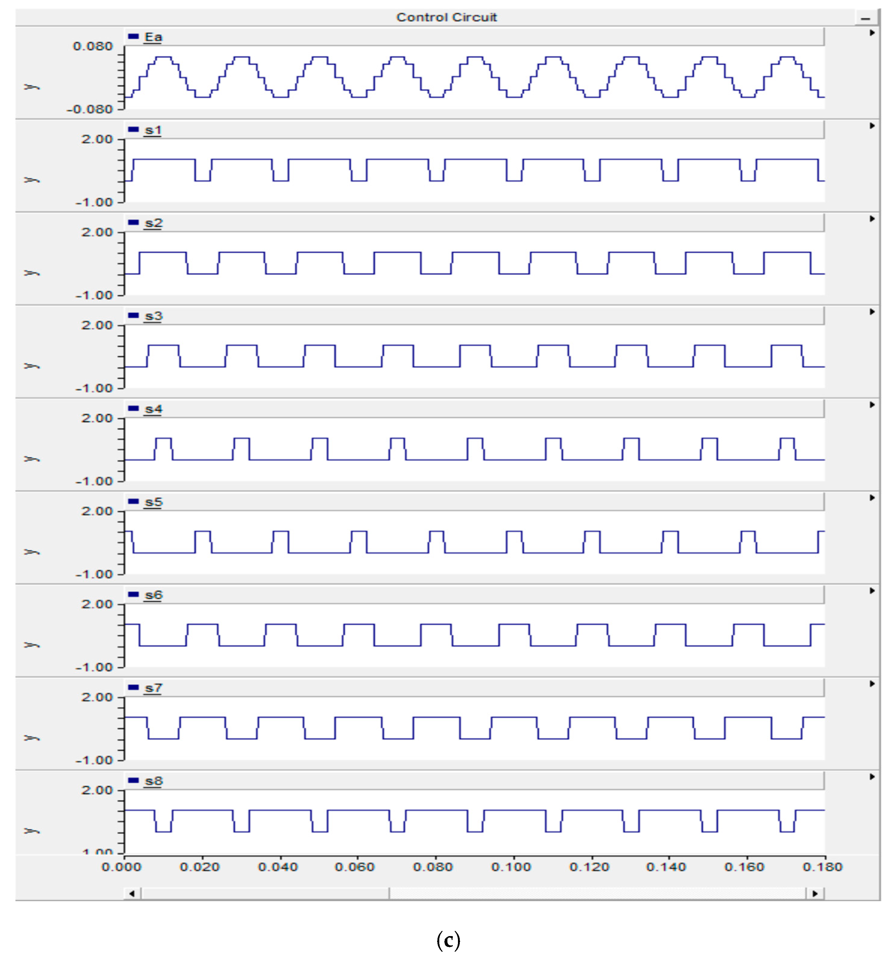
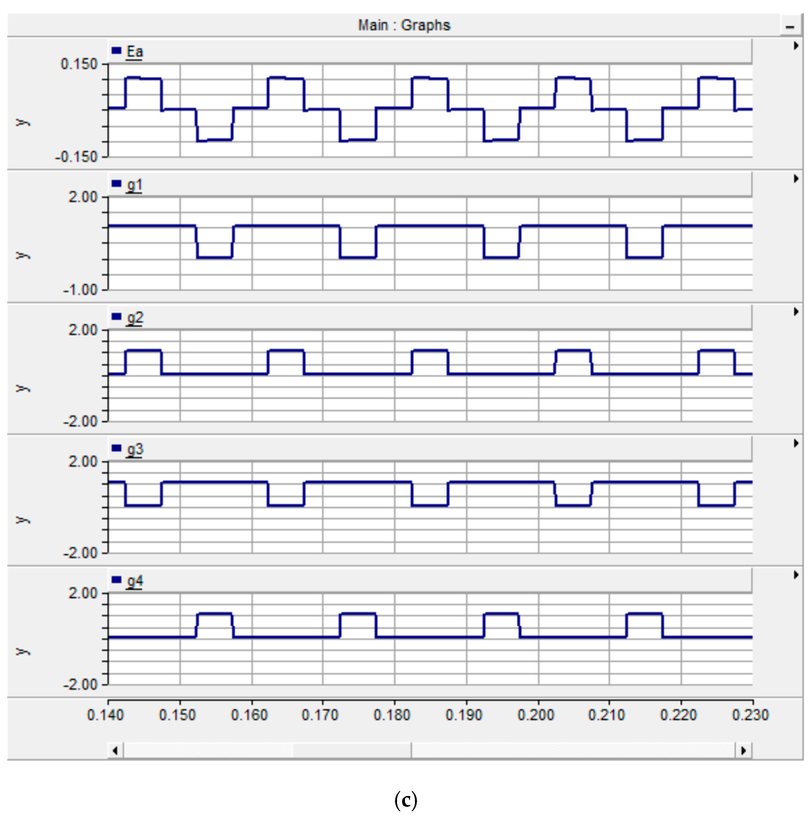
2.3.1. Three-Level FC-MLI PSCAD Simulations

In Figure 10b, the control circuit with two gate signals of g1 and g2 are available. Another two are obtained using the NOT gate with initial two signals. These four signals are ready to give to IGBT which are in the 3-level FC-MLI power circuit.
In Figure 10a, all the gate pulses are applied to the different IGBT of FC-MLI following Table 5 of a sequence of a waveform for gate signals. For Vdc; switched g1 and g4 are conduct. For 0Vdc; g1 and g3 are conducted and for −Vdc; g3 and g4 are conducted.

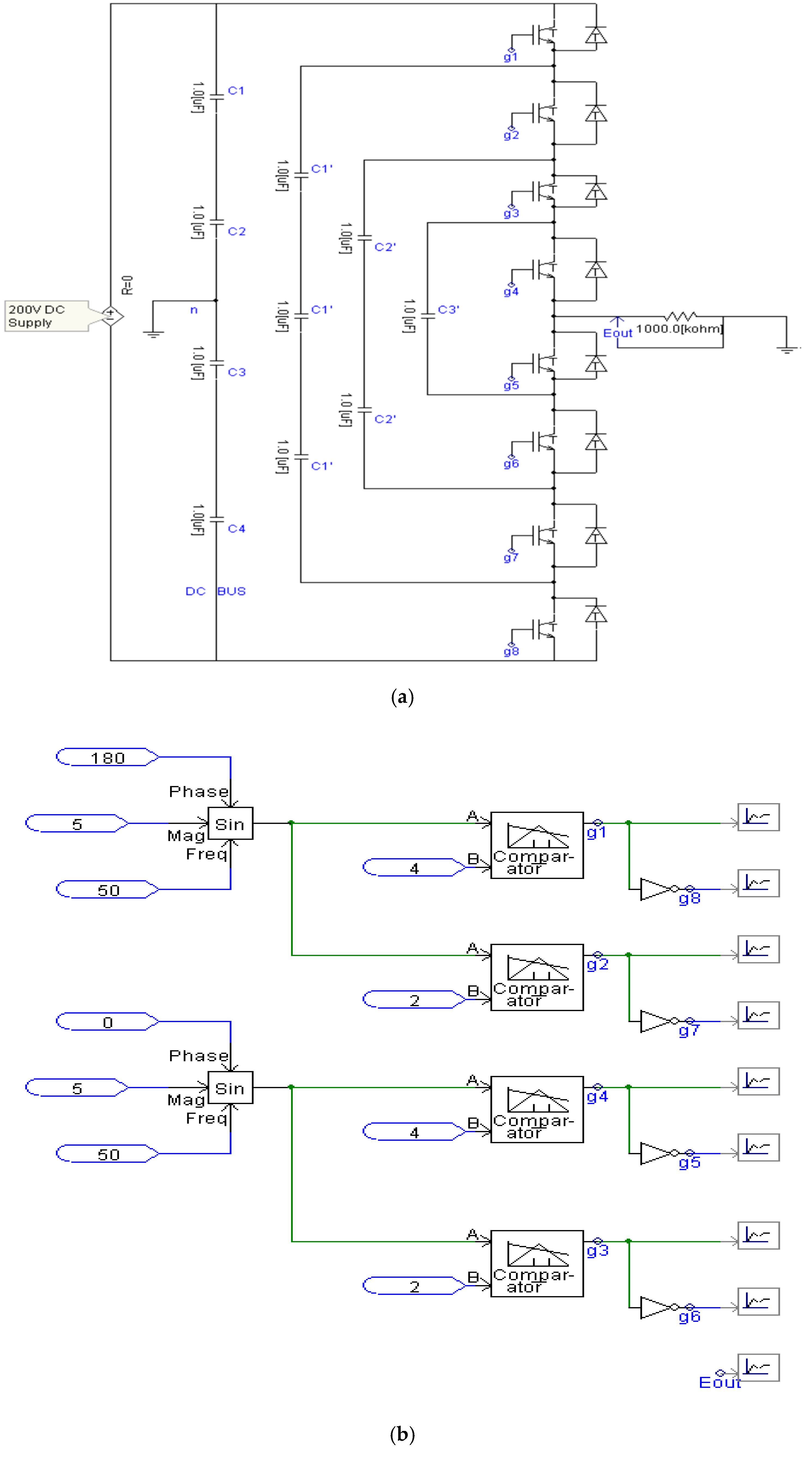
2.3.2. Five-Level FC-MLI PSCAD Simulations

Figure 11b, the control circuit waveforms are generated by comparison of the DC signal (2 V and 4 V) with the sinusoidal waveforms (5 V RMS). Changing the values of the DC voltage will change the gate pulse widths. Four signals g1, g2, g3, and g4 are available from the direct comparator. The other four signals are obtained using the NOT with initial four signals. These 8 gate signals are ready to give to IGBT which are in the FC-MLI power circuit.
In Figure 11a, all the available gate signals are given to IGBT of FC-MLI Inverter, following Table 6 of the sequence of a waveform for gate signals. Here the total voltage is divided into a capacitor bridge. Each capacitor (C1, C2, C3, and C4) of the first line gets charged with Vdc/4 voltage. Also, each intermediate capacitor (C1’, C2’, and C3’) gets charged by +Vdc/4.
+Vdc/2: Switched g1, g2, g3, and g4 are turned ON. Hence, current flow from capacitor C2, C1, g1, g2, g3, g4 to the load. Hence, by two capacitor-discharge, (+Vdc/4 +Vdc/4) = +Vdc/2 is available at load side. +Vdc/4: Similarly, g1, g2, g3, and g5 are turned on. Current flows, from capacitor C2, C1, g1, g2, g3, C3’ and g5 to the load. Hence the voltage across the load is Vdc/4. In other words, C3’ nullifies the voltage from one of the capacitors (C1 or C2) to load voltage. Hence only half voltage (of +Vdc/2) is available at the load. 0Vdc: g1, g2, g5, g6 are turned on. Similar to the previous operation, both C2’ capacitors provide the opposite voltage to C1 and C2. Hence equivalent voltage at the load is 0, −Vdc/4: g1, g5, g6, g7 are turned on. Current flows through the C2, C1, g1, C2’, C2’, C2’, g5, g6, g7, and load. Now here two capacitors charged with +Vdc/4, +Vdc/4, and three capacitors are in opposite direction and charged by +Vdc/4, +Vdc/4, +Vdc/4 hence the effective voltage at the load is (+2Vdc/4) – (+3Vdc/4) = −Vdc/4. −Vdc/2: g5, g6, g7, g8 are turned ON. Current flows from C4, C3 to load (reverse direction) Back to C4. Hence, the voltage of two capacitors is available at load side (−Vdc/4 + (−Vdc/4) = −Vdc/2.

3. Performance Evaluations of Different Multilevel Inverters and Characteristics Overview

The various topologies discussed, described, and analyzed till now are comprehensively compared in this section on the basis of different performance parameters such as number capacitors and diodes, switches, flexibility, balancing capacitor, and cost in Table 7.
For high-voltage applications, for instance high-voltage DC (HVDC), a relatively high voltage level can be chosen for a modular multilevel inverter [5,32,33,34,35,36,37,38,39,40,41,42,43,44,45,46,47,48,49,50,51,52,53] to the total required current THD, and dv/dt. For medium- and low-voltage applications, five and three-level inverters for A-NPC [54,55,56,57,58] and other FC-MLI inverters may be better suited to current specifications. Currently, multilevel inverters have been suggested in motor drives, flexible AC transmission systems (FACTS) and HVDC. As per the studies conducted in [2,59,60,61,62,63,64,65,66,67], the positive points, negative points, methods of modulation, and application of these inverters are epitomized in Table 8.

3.1. Choosing Topology

Discussed all multilevel inverters are utilized to generate a smooth waveform, mostly for medium voltage drives. Out of three FC-MLI [19,77,78,79,80,81,82] is relatively new compared to DC-MLI and CHB-MLI. Moreover, FC-MLI has some unique benefits over DC-MLI, including the truancy of clamp diodes and the ability to adjust the voltage of the flying capacitor by selecting an excess state. Even the voltage level is higher than 3 [81]. Unlike CHB-MLI, no separate voltage sources are required. Also, there are two types having some deficiencies, such as most DC in CHB-MLI. Losses are higher in the DC-MLI. but FC-MLI has introduced more potential outcomes to regulate the DC-link capacitor’s voltage contrasting to another multilevel topology that uses redundant switching arrangements. An FC-MLI topology is designed for higher voltage and lower voltage-distortion performance. Moreover, in an FC-MLI, capacitors are using for clamping the power over the devices. Also, FC-MLI is appropriate to heavy load systems. Meanwhile, induction motors are utilizing as a load in many industrial applications [78].

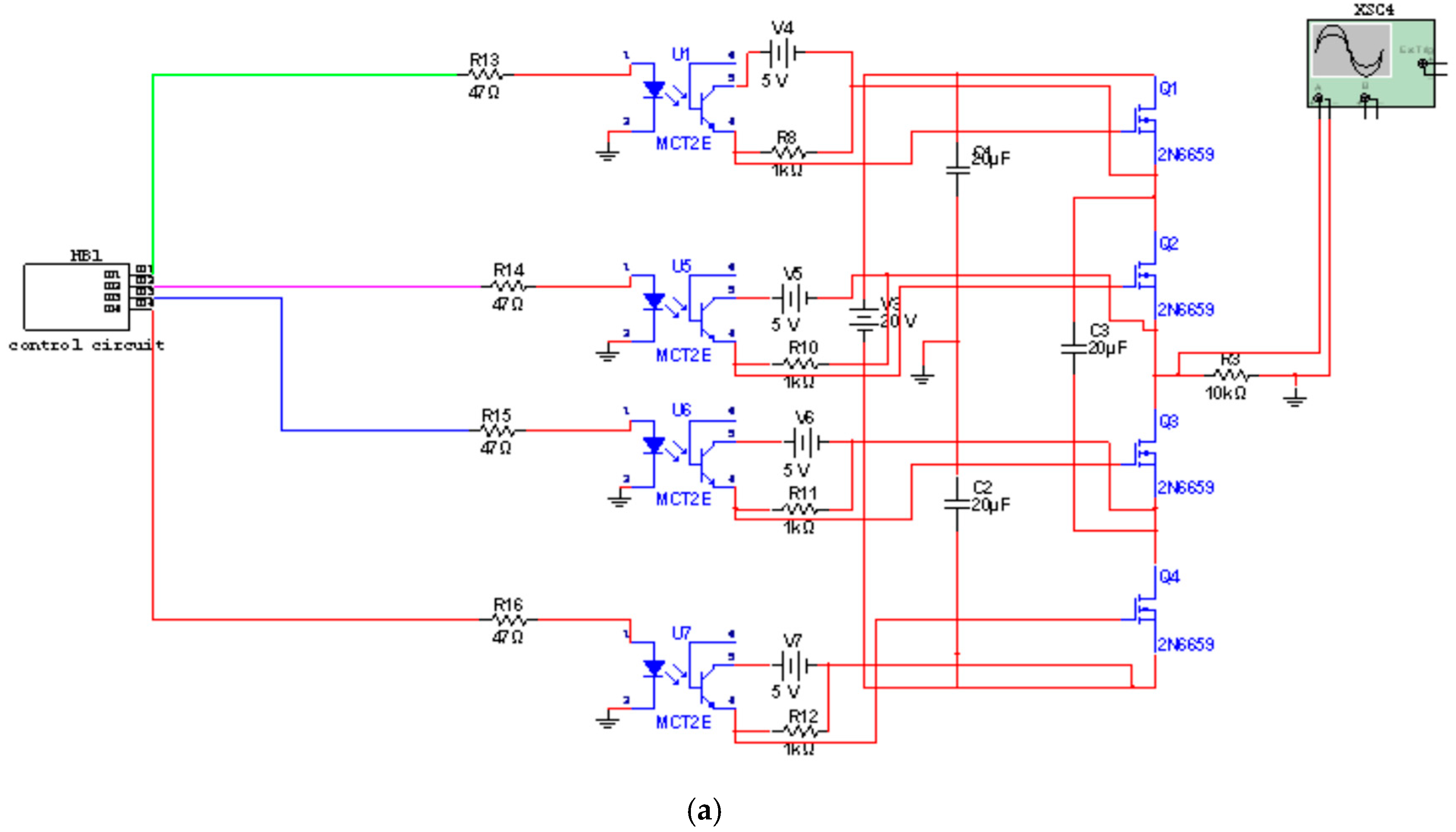
3.2. MULTISIM Simulations of FC-MLI

3.2.1. Three-Level FC-MLI MULTISIM Simulations

In the above Figure 12a, the control circuit has a hierarchical block which will be explained in the next section. Here, the same power circuit is used as the above explained. There are three capacitors. Among three capacitors, two capacitors make the DC bus and remaining capacitor acts as a flying capacitor which is used for the clamping voltage at different levels. Here we have used 20 V DC as source power supply. There are four MOSFET switches which are triggered by the gate pulses that generate from the control circuit. Four optocouplers MCT 2E are used for the isolation purpose.
We have generated four gate pulses using the OP-AMPs. In Figure 12b, we have used one OP-AMP as a ZERO CROSSING DETECTOR and another as a SCHMITT TRIGGER. The output of the SCHMITT TRIGGER is a square wave but shifted from the output of the ZERO CROSSING DETECTOR (ZCD). The shifting can vary by varying the POT of 50Kohm. If the shifting is higher than the output, that has the higher width of zero pulses.
As in Figure 13. we can see the all 3 levels of output. Here we used 20 V DC as a power source, therefore we have 2 different levels of (Vdc/2) =10 V, and (−Vdc/2) = −10 V. By changing the DC voltage in the OP-AMP comparator, we can change the width of output zero voltage. This width of zero voltage decides the amount of reactive power flow in the system.

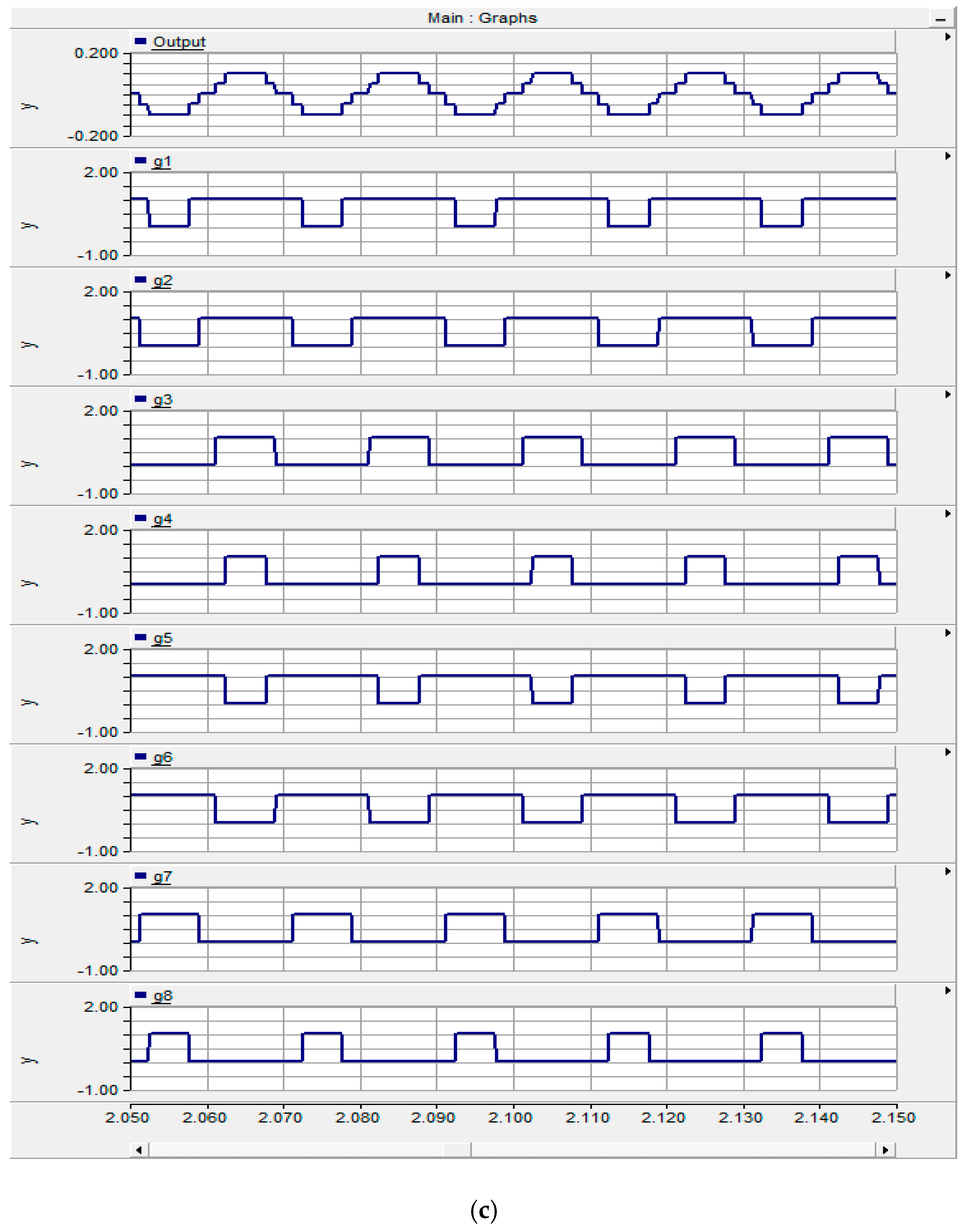
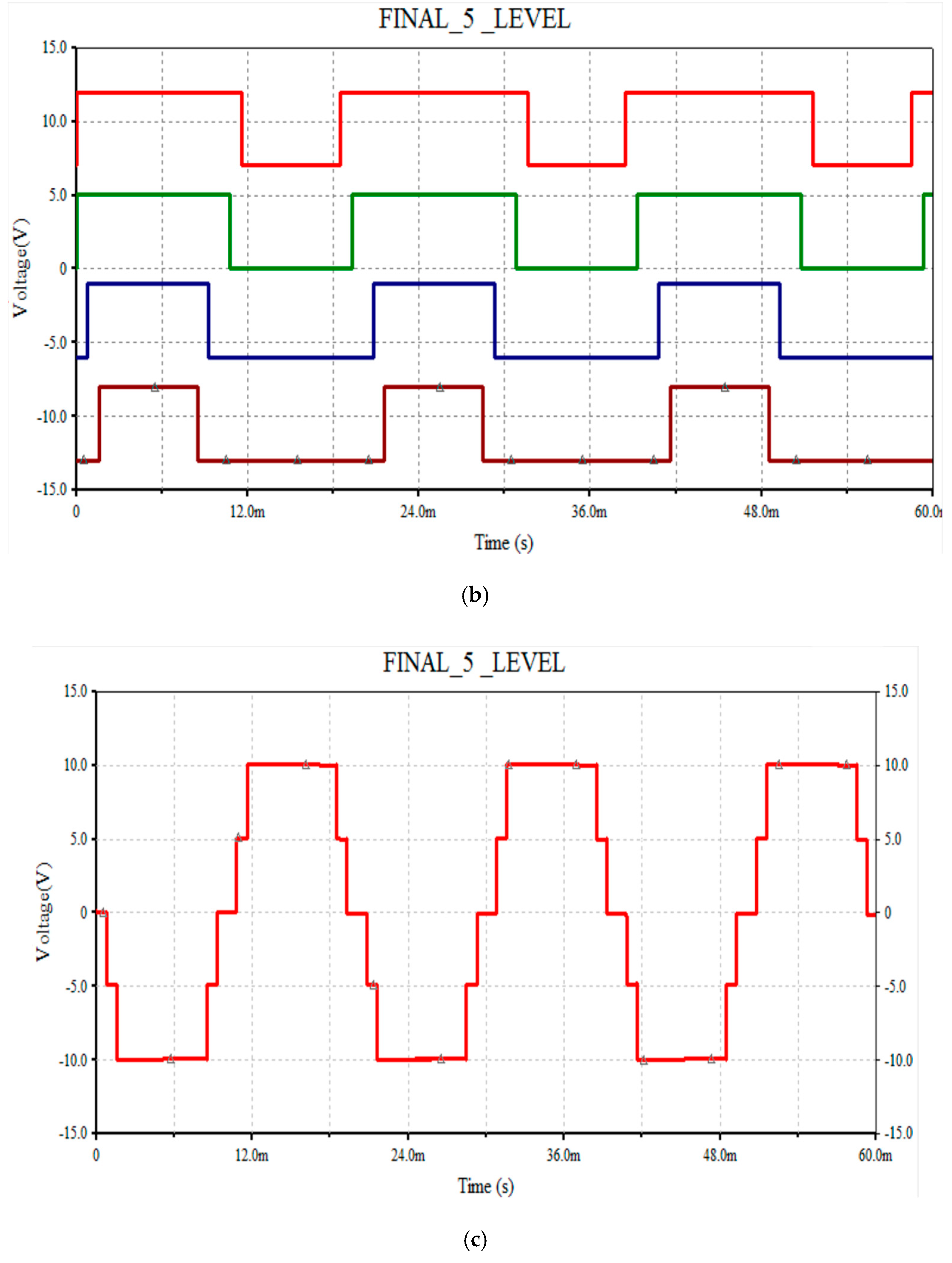
3.2.2. 5-Level FC-MLI MULTISIM Simulations

The full set-up is shown in Figure 14a. That is divided into the following two parts. That diagram is the same as explained above. Here, we have used MOSFET 2N6659 as a switching device. And the similar three-level optocoupler MCT 2E is used for isolation. We have demonstrated the purely resistive load for the simplicity. We can change the load as per the relevant applications.
Now as the above explained theory, 4 switches get turning on at any time and remaining four switches get turning off at any time what you want. Therefore, each switch gets 1/4th voltage of power supply as a reverse burden.
Figure 14b for the control circuit, we have used the two sinusoidal power supplies as the reference by comparing it with DC power supply. We have four different outputs having four gates from the required eight pulses. We can obtain the NOT gate combination from the remaining four pulses. Thus, we can get eight pulses and these pulses are applied to the power circuit through an optocoupler.
In Figure 15a–c we can see all the 5-levels output and gate pulses. Here we have used 20 V DC. As a source, we have 4 different levels of (Vdc/2) = 10 V, (Vdc/4) = 5 V, 0 V, (−Vdc/4) = −5 V, (Vdc/2) = −10 V. By changing the DC. voltage in the OP-AMP comparator; we can change the width of zero for output voltage. This width of zero voltage decides the amount of reactive power flow in the system.

4. Harmonics Analysis of FC-MLI

4.1. Total Harmonic Distortion (THD)

The THD is a presenting measurement of harmonic distortion and defined the proportion between harmonic components and the fundamental frequency of the power. THD is utilized to characterize the linearity of audio systems and the power quality of electric systems.
If the input signal is sinusoidal, the computation often corresponds to the proportion of the powers of all the harmonic frequencies beyond the power of the 1st harmonic and the main frequency.
T H D = P 2 + P 3 + P 4 + + P P 1 = i = 2 P i P 1
Which can equivalently be written as:
T H D = P t o t a l P 1 P 1
It is also defined as the amplitude ratio, not the power ratio which results in the determination of THD given the square root to the above equation.
T H D = V 2 2 + V 3 2 + V 4 2 + + V 2 V 1

4.1.1. Harmonics Analysis of 3-Level FC-MLI

As shown in Figure 16, the analysis can be seen that for lower order mainly 5th and 7th harmonics are predominant. Here the third harmonic has been reduced very much.
If we change the pulse width of our gate pulses then the harmonic reduction can be changed; more specifically, THD can be changed. Because of changing our pulse width, the starting angle of output wave changes and thus the harmonics also changes. However, if we compare this with conventional two-level inverter then we cannot find any harmonics in this topology compared with the two-level inverter.
In Table 9 shows the analysis of THD. The total harmonic distortion shows that how much percentage harmonics are present in the waveform or how much the waveform is disturbed from an actual sine wave.
The following analysis is carried out by the MULTISIM software; here, we have found 15 numbers of harmonics. While analyzing; the sampling frequency is taken as 16 kHz. This analysis is also carried out with Lagrange’s 1st degree of interpolation.
The above tabulated analysis gives us that mainly 5th and 7th harmonics are the predominating and has a major part in THD normal magnitude. A phase is measured by taking the fundamental 50 Hz as a reference.

4.1.2. Harmonics Analysis of 5-Level FC-MLI

In Figure 17, the analysis shows that the major 3rd harmonics is predominant but all other has very low impact. Hence, here THD is also less as given in Table 10.
Table 10 shows the analysis of THD. Here, only 3rd harmonic is predominating, and all others are much lower. Now if we change the width of gate pulses the THD can be further reduced. One thing to note is that in 3-level the THD was 28.88% while in the 5-level topology the THD is 18.56%. Hence by increasing the levels of the output, we can reduce the total harmonics distortion. Therefore, if the number of levels are increased, then THD is decreased.

5. Pulse width modulation (PWM) control techniques

Depending on the control strategy, the most important two types of the PWM modulation techniques are categorized as open and closed loop. SPMW, PWM space vector, sigma-delta modulation (SDM) are the part of open-loop PWM methods, and hysteresis, optimized current control; linear methods are identified by closed-loop current control methods.

5.1. Open-Loop PWM Control Techniques

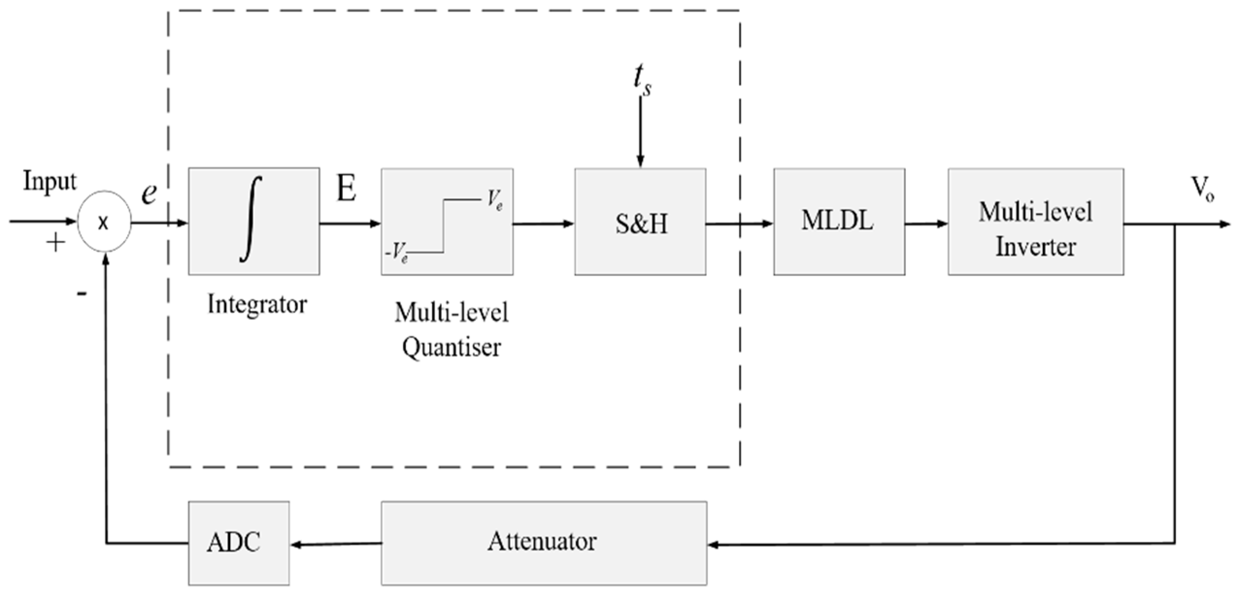
5.1.1. Sigma Delta PWM (SDM)

The SDM method was first classified by Jager in 1952 as a 1-bit PCM (pulse code modification) coding method. A 1-bit coding application is created utilizing the integrated feedback block on a pulse modulator, which is part of the encoding process, as shown in Figure 18a [83]. Sigma delta modulation originally suggested as a way to encode 1-bit audio and video signals in digital control and modulation problems. SDM has been classified to avoid a decrease in the power density of the altered signals with an increase in the sampling frequency. An SDM method was acquired by adding a test and restraint unit to the main SDM modulator, as shown in Figure 18b.
SDM modified the energy transformation operation utilizing analog to digital converters, which are widely used in some applications because of the expansion of semiconductor technologies. Using an inverter with resonant DC-link permits using soft switching applications rather than hard PWM switching. This type of inverter is mainly known as zero switching losses acquired through switching to the present time, and this technique can be adjusted according to the SDM. In Figure 18b, the modulator output signal varies between +Vo, 0 and Vo depending on the sampling period of fs, and the output signal is compared to the amplitudes of input. The result of the comparison (e) is integrated (E) and the quantizer decide the output signal across from E. The multilevel SDM creates a multi-bit data stream and the output decode creates various output states that might be utilized to regulate the activate/deactivate states of multilevel inverter switches. Figure 19 shows a schematic diagram of a multilevel inverter regulated by SDM. The interaction between the SDM modulator and the inverter is controlled by a multilevel decoding logic block, which receives the SDM signals and decodes the inverter switching signals [84,85,86].
Studies show that it designed to regulate DC link inverter, SDM might be expanded to regulate multilevel inverters via logical interface. For SDM-regulated multilevel inverters, output faults, for instance, unequal voltage distribution and system imbalances, might be decreased to a high switching frequency up to 200 kHz.

5.1.2. Sinusoidal PWM (SPWM)

The most widely used method among many PWM techniques is the SPWM out of other power switching inverters. In the SPWM, the sine wave of the source voltage when compared to a carrier wave of triangular type to produce gate signals for the inverter switch. Energy debauchery can be considered a major problem for high-power applications. A basic SPWM frequency control method has been suggested to reduce the switching losses. SPWM multi-carrier regulate method has also been executed to enhance the performance of operated multilevel inverters and is categorized as per perpendicular or horizontal carrier signal adjustment. Perpendicular carrier distribution methods are called phase dissipation (PD), phase opposition (POD) and alternative phase dissipation (APOD); however, the horizontal arrangement is called the phase shift control method (PS). Even though PS-PWM is only useful for CHB-MLI and FC-MLI, PD-PWM is more useful for DC-MLI [87].
From the above discussion, multicarrier SPWM regulates methods is shown in Figure 20a PD, (b) POD, (c) APOD, (d) PS. SPWM is the mainly utilized PWM control technique because of its many advantages, such as the simple implementation of lower harmonic output signals per other methods and lower transmission dissipations. In the SPWM, a high-frequency triangular carrier signal is analyzed to a low-frequency sine wave signal in an analog or digital device. The frequency of the sine wave modulation signal determines the required frequency of the line voltage at the output of the inverter [88].

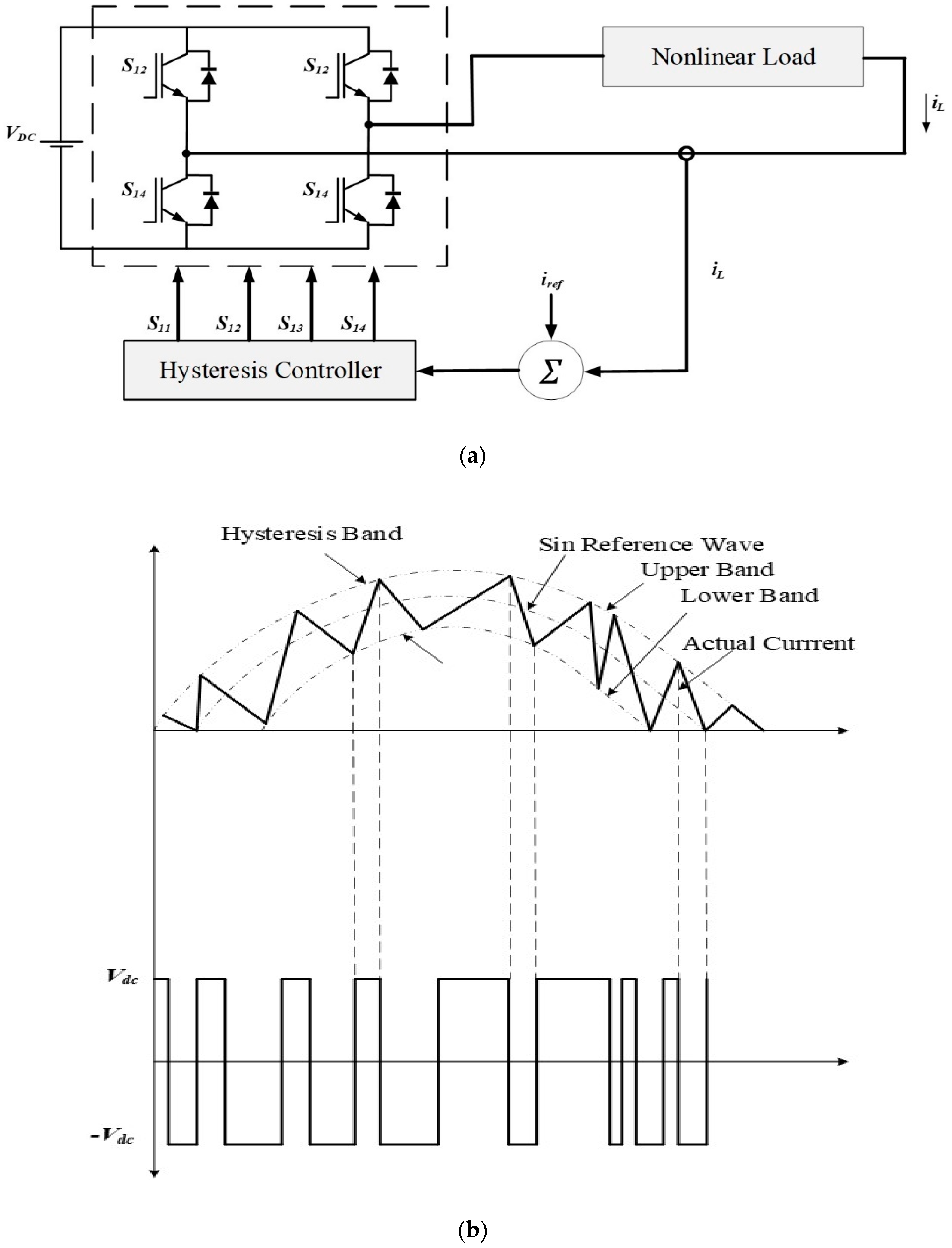
5.2. Closed-Loop PWM Control Techniques

Most widely used applications of PWM converters, like drives of a motor, active filters and many more, need a control form consisting of an inner current feedback loop. A multilevel inverter system uses photovoltaic (PV) or wind power sources to combine renewable power sources into the grid. Several methods have been conducted to reduce harmonics by utilizing current regulate for active power filter or by connecting a photoelectric and wind generator integrated to grid applications of a multilevel inverter. Current control methods are primarily discussed in terms of hysteresis current control and line current control [89,90,91,92].
Hysteresis modulation is a current regulate technique in which the load current follows the reference current in the hysteresis band in non-linear load application of multilevel inverter. Figure 21a is a schematic layout of the hysteresis regulation of the H-bridge, and Figure 21b illustrates the fundamental law of the hysteresis modulation. The employed controller creates a sinusoidal source current that of desired magnitude and also frequency, which is analyzed according to the actual current. If the current surpasses the higher level of the hysteresis band, it must choose the next higher voltage level to try to force the current error to zero. However, the voltage level of the inverter might be not enough to reset the current error to zero, and the inverter must move to the further higher voltage level to obtain the correct voltage level. Consequently, the current returns to the hysteresis band and the current follow the reference current in the hysteresis band. The three hysteresis controllers correctly select the voltage level are explained as offset band three-level, double band three-level, and time-based three-level hysteresis controllers [86,91,92,93,94].
Considering this to be a different method of multilevel inverter usage, the grid connection to the inverter must need current regulating. Linear current regulators are categorized as ramp comparators, stationary vector, and synchronous vector regulator. The ramp regulator uses the output ripple and feedback to regulate the switching instantly. In a 3-phase isolated neutral load method, the 3-phase current must have a zero-sum. Thus, linear compensation and the required two reference voltages of a three-phase inverter can be determined by utilizing 2 to 3 phase AB/ABC conversion blocks as shown in Figure 22.
The main linear current regulator comprises a tracking controller with an equivalent integrator for photovoltaic converters. Numerous harmonic compensation strategies can be found in the following articles on re-control and a linear resonant harmonic compensator [86,95,96,97].

6. Conclusions

Many researchers and industries have acquired a multilevel inverter because of the capacities to regulate high- and medium-power applications. Also, the sustainable power source of DC needs to be changed over to AC. We demonstrate three different types of multilevel inverter, such as a cascade H multilevel inverter, a diode-clamp multilevel inverter, and a flying-capacitor multilevel inverter. Although all multilevel inverters are utilized to produce smoothing signals, the two types mentioned above have some drawbacks. For example, the individual DC sources are required for each inverter in CHB-MLI inverter and DC-MLI inverter switching losses are higher. These topologies are modeled in PSCADS SIMULINK. However, a flying-capacitor multilevel inverter has several features to regulate DC link capacitors compared to another multilevel topology using redundant switch configurations. From the MULTISIM simulation analysis and modeling of a flying-capacitor multilevel inverter in three levels, THD was 28.88% while in the five-level topology the THD was 18.56%. Therefore, we can decrease the total harmonic distortion adopting the higher-level topology.

Author Contributions

This paper was a collaboration effort among all authors. All authors conceived the methodology, conducted the experiment tests, and wrote the paper. R.A.R. and S.A.P. analyzed, designed and development of the experiment methodologies, A.M. and C.w.L. supported the work to perform in real time and, H.-J.K. verified the overall experiment.

Funding

This research was supported by Basic Research Laboratory through the National Research Foundations of Korea funded by the Ministry of Science, ICT and Future Planning (NRF-2015R1A4A1041584).

Conflicts of Interest

The authors declare no conflict of interest.

References

  1. Rashid, M.H. Power Electronics Circuits, Devices and Application Handbook, 3rd ed.; Pearson Education: Upper Saddle River, NJ, USA, 2003. [Google Scholar]
  2. Rodriguez, J.; Jih-Sheng, L.; Fang, P. Multilevel inverters: A survey of topologies, controls, and applications. IEEE Trans. Ind. Electron. 2002, 49, 724–738. [Google Scholar] [CrossRef]
  3. Raghavendra, R.K.; Vijay, B.B.; Hiralal, M.S. A three-phase hybrid cascaded modular multilevel inverter for renewable energy environment. IEEE Trans. Power Electron. 2016, 32, 1070–1078. [Google Scholar]
  4. Youssef, O.; Kamal, A.H.; Luc-Andre, G. Packed u cells multilevel converter topology: Theoretical study and experimental validation. IEEE Trans. Ind. Electron. 2011, 58, 1294–1306. [Google Scholar]
  5. Sumit, K.C.; Chandan, C. A new asymmetric multilevel inverter topology suitable for solar PV applications with varying irradiance. IEEE Trans. Sustain. Energy 2017, 8, 1496–1506. [Google Scholar]
  6. Vahid, D.; Arash, K.S.; Mostafa, A.; Soheila, E.; Keith, A.C. A new family of modular multilevel converter based on modified flying-capacitor multicell converters. IEEE Trans. Power Electron. 2015, 30, 138–147. [Google Scholar]
  7. Vahid, D.; Saeedeh, D. Analytical modelling of single-phase stacked multicell multilevel converters exploiting kapteyn (fourier–bessel) series. IET Power Electron. 2013, 6, 1220–1238. [Google Scholar]
  8. Arash, K.; Vahid, D.; Mostafa, A.; Saeedeh, D. Reduced dc voltage source flying capacitor multicell multilevel inverter: Analysis and implementation. IET Power Electron. 2014, 7, 439–450. [Google Scholar]
  9. Arash, K.; Mostafa, A.; Keith, A.C.; Vahid, D. A new breed of optimized symmetrical and asymmetrical cascaded multilevel power converters. IEEE J. Emerg Sel. Top. Power Electron. 2015, 3, 1160–1170. [Google Scholar]
  10. Saeedeh, D.; Ebrahim, B.; Soheila, E.; Vahid, D.; Mehran, S. Flying-capacitor stacked multicell multilevel voltage source inverters: Analysis and modelling. IET Power Electron. 2014, 7, 2969–2987. [Google Scholar]
  11. Arash, K.; Vahid, D.; Keith, A.C. New flying-capacitor-based multilevel converter with optimized number of switches and capacitors for renewable energy integration. IEEE Trans. Energy Convers 2016, 31, 846–859. [Google Scholar]
  12. Margarita, N.; Samir, K.; Sibylle, D.; Jose, R. Reduced multilevel converter: A novel multilevel converter with a reduced number of active switches. IEEE Trans. Ind. Electron. 2018, 65, 3636–3645. [Google Scholar]
  13. Amir, T.; Jafar, A.; Mohammad, R. A multilevel inverter structure based on a combination of switched capacitors and dc sources. IEEE Trans. Ind. Inform. 2017, 13, 2162–2171. [Google Scholar]
  14. Meysam, S.; Jafar, A.; Seyyed, M.H. Cascaded multilevel inverter based on symmetric asymmetric dc sources with reduced number of components. IET Power Electron. 2017, 10, 1468–1478. [Google Scholar]
  15. Reza, B.; Majid, M.; Elyas, Z.; Hossein, M.K.; Frede, B. A new boost switched-capacitor multilevel converter with reduced circuit devices. IEEE Trans. Power Electron. 2017, 33, 6738–6754. [Google Scholar]
  16. Krishna, K.G.; Alekh, R.; Pallavee, B.; Lalit, K.S.; Shailendra, J. Multilevel inverter topologies with reduced device count: A review. IEEE Trans. Power Electron. 2016, 31, 135–151. [Google Scholar]
  17. Kavitha, M.; Arunkumar, A.; Gokulnath, N.; Arun, S. New Cascaded H-Bridge Multilevel Inverter Topology with Reduced Number of Switches and Sources. IOSR-JEEE 2012, 2, 26–36. [Google Scholar] [CrossRef]
  18. Ke, Ma.; Frede, B. Modulation Methods for Neutral-Point-Clamped Wind Power Converter Achieving Loss and Thermal Redistribution under Low-Voltage-Ride-Through. IEEE Trans. on Ind. Electron. 2013, 61, 835–845. [Google Scholar]
  19. Hochgra, C.; Lasseter, R.; Divan, D.; Lipo, T.A. Comparison of multilevel inverters for static VAR compensation. In Proceedings of the IEEE Industry Applications Society Annual Meeting, Denver, CO, USA, 2–6 October 1994. [Google Scholar]
  20. Kuhn, H.; Rüger, N.E.; Mertens, A. Control strategy for multilevel inverter with non-ideal dc sources. In Proceedings of the IEEE Power Electronics Specialists Conference, Orlando, FL, USA, 17–21 June 2007. [Google Scholar]
  21. Panagis, P.; Stergiopoulos, F.; Marabeas, P.; Manias, S. Comparison of state-of-the-art multilevel inverters. In Proceedings of the IEEE Annual Power Electronics Specialist Conference PESC, Rhodes Greece, 15–19 June 2008. [Google Scholar]
  22. Sumithira, T.R.; Nirmal, A. Elimination of harmonics in multilevel inverters connected to solar photovoltaic systems using ANFIS: An experimental case study. Appl. Res. Technol. 2013, 11, 124–132. [Google Scholar] [CrossRef]
  23. Jih-Sheng, L.; Fang, P. Multilevel converters-a new breed of power converters. IEEE Trans. Ind. Appl. 1996, 32, 509–517. [Google Scholar] [CrossRef]
  24. Mohammadreza, D. Analysis of Different Topologies of Multilevel Inverter Thesis; Chalmers University of Technology: Gothenburg, Sweden, 2010. [Google Scholar]
  25. Khairnar, D.D.; Deshmukh, V.M. Performance Analysis of Diode Clamped 3 Level MOSFET Based Inverter. Int. Electr. Eng. J. 2014, 5, 1484–1489. [Google Scholar]
  26. Mehdi, N.; Bin, W.; Navid, R. A Novel Five level voltage source inverter with sinusoidal pulse width modulator for medium voltage applications. IEEE Trans. Power Electron. 2016, 31, 1959–1967. [Google Scholar]
  27. Kai, T.; Bin, W.; Mehdi, N.; Xu, D.D.; Cheng, Z.; Navid, R. A Capacitor voltage balancing method for Nested neutral point clamped (NNPC) inverter. IEEE Trans. Power Electron. 2015, 31, 2575–2583. [Google Scholar]
  28. Song, B.M.; Kim, J.; Lai, J.S.; Seong, K.C.; Kim, H.J.; Park, S.S. A multilevel soft-switching inverter with inductor coupling. IEEE Trans. Ind. Appl. 2001, 37, 628–636. [Google Scholar] [CrossRef]
  29. Meynard, T.A.; Foch, H. Multi-level conversion: High voltage choppers and voltage-source inverters. In Proceedings of the IEEE Power Electronics Specialists Conference, Toledo, Spain, 29 June–3 July 1992. [Google Scholar]
  30. Xu, L.; Agelidis, V.G. Active capacitor voltage control of flying capacitor multilevel converters. IEEE Electr. Power Appl. 2004, 151, 313–320. [Google Scholar] [CrossRef]
  31. Feng, C.; Liang, J.; Agelidis, V.G.; Green, T.C. A multi-modular system based on parallel-connected multilevel flying capacitor converters controlled with fundamental frequency SPWM. In Proceedings of the 32nd IEEE Conference on Industrial Electronics, Paris, France, 7–10 November 2006. [Google Scholar]
  32. Nami, A.; Liang, J.; Dijkhuizen, F.; Demetriades, G.D. Modular multilevel converters for HVDC applications: Review on converter cells and functionalities. IEEE Trans. Power Electron. 2015, 30, 18–36. [Google Scholar] [CrossRef]
  33. Hiller, M. Method for Controlling a Polyphase Converter with Distributed Energy Stores. U.S. Patent 12/067, 555, 20 March 2008. [Google Scholar]
  34. Ilves, K.; Taffner, F.; Norrga, S.; Antonopoulos, A.; Harnefors, L.; Nee, H.-P. A submodule implementation for parallel connection of capacitors in modular multilevel converters. IEEE Trans. Power Electron. 2015, 30, 3518–3527. [Google Scholar] [CrossRef]
  35. Farhadi, M.; Babaei, E. Cross-switched multilevel inverter: An innovative topology. IET Trans. Power Electron. 2013, 6, 642–651. [Google Scholar] [CrossRef]
  36. Mathew, E.C.; Ghat, M.B.; Shukla, A. A generalized cross-connected submodule structure for hybrid multilevel converters. IEEE Trans. Ind. Appl. 2016, 52, 3159–3170. [Google Scholar] [CrossRef]
  37. Wang, Y.; Marquardt, R. Future HVDC-grids employing modular multilevel converters and hybrid DC-breakers. In Proceedings of the 15th European Conference on Power Electronics and Applications (EPE), Lille, France, 3–5 September 2013. [Google Scholar]
  38. Marquardt, R. Modular multilevel converter topologies with DC-short circuit current limitation. In Proceedings of the 8th International Conference on Power Electronics—ECCE Asia, Jeju, Korea, 30 May–3 June 2011. [Google Scholar]
  39. Li, X.; Song, Q.; Liu, W.; Zhu, Z.; Xu, S. Experiment on DC-fault ride through of MMC using a half-voltage clamp submodule. IEEE J. Emerg. Sel. Top. Power Electron. 2018, 6, 1273–1279. [Google Scholar] [CrossRef]
  40. Elserougi, A.A.; Massoud, A.M.; Ahmed, S. A switched-capacitor submodule for modular multilevel HVDC converters with DC-fault blocking capability and a reduced number of sensors. IEEE Trans. Power Del. 2016, 31, 313–322. [Google Scholar] [CrossRef]
  41. Qin, J.; Saeedifard, M.; Rockhill, A.; Zhou, R. Hybrid design of modular multilevel converters for HVDC systems based on various submodule circuits. IEEE Trans. Power Del. 2015, 30, 385–394. [Google Scholar] [CrossRef]
  42. Nami, A.; Wang, L.; Dijkhuizen, F.; Shukla, A. Five level cross connected cell for cascaded converters. In Proceedings of the 2013 15th European Conference on Power Electronics and Applications (EPE), Lille, France, 3–5 September 2013. [Google Scholar]
  43. Li, R.; Fletcher, J.E.; Xu, L.; Holliday, D.; Williams, B.W. A hybrid modular multilevel converter with novel three-level cells for DC fault blocking capability. IEEE Trans. Power Del. 2015, 30, 1853–1862. [Google Scholar] [CrossRef]
  44. Hu, X.; Zhang, J.; Xu, S.; Jiang, Y. Investigation of a new modular multilevel converter with DC fault blocking capability. IEEE Trans. Ind. Appl. 2018, 55, 552–562. [Google Scholar] [CrossRef]
  45. Chattopadhyay, S.K.; Chakraborty, C. Multilevel inverters with level doubling network: A new topological variation. In Proceedings of the Industrial Electronics Society Conference, Vienna, Austria, 10–14 November 2013. [Google Scholar]
  46. Chattopadhyay, S.K.; Chakraborty, C. A new multilevel inverter topology with self-balancing level doubling network. IEEE Trans. Ind. Electron. 2014, 61, 4622–4631. [Google Scholar] [CrossRef]
  47. Ji, Y.; Chen, G. A novel three-phase seven-level active clamped converter using H-bridge as a level doubling network. In Proceedings of the IEEE 8th International Power Electronics and Motion Control Conference, IPEMC-ECCE Asia, Hefei, China, 22–26 May 2016. [Google Scholar]
  48. Rajesh, V.; Chattopadhyay, S.K.; Chakraborty, C. Full bridge level doubling network assisted multilevel DC link inverter. In Proceedings of the IEEE 7th Power India International Conference, PIICON 2016, Bikaner, India, 25–27 November 2017. [Google Scholar]
  49. Agelidis, V.G.; Demetriades, G.D.; Flourentzou, N. Recent advances in high-voltage direct-current power transmission systems. In Proceedings of the 2006 IEEE International Conference on Industrial Technology, Mumbai, India, 15–17 December 2006. [Google Scholar]
  50. Akagi, H. Classification, terminology, and application of the modular multilevel cascade converter (MMCC). IEEE Trans. Power Electron. 2011, 26, 3119–3130. [Google Scholar] [CrossRef]
  51. Hu, X.; Zhang, J.; Xu, S.; Jiang, Y. Extended state observer-based fault detection and location method for modular multilevel converters. In Proceedings of the IECON 42nd Annual Conference of the IEEE Industrial Electronics Society, Florence, Italy, 23–26 October 2016. [Google Scholar]
  52. Pérez, M.; Rodríguez, J.; Pontt, J.; Kouro, S. Power distribution in hybrid multi-cell converter with nearest level modulation. In Proceedings of the IEEE International Symposium on Industrial Electronics, 4–7 June 2007. [Google Scholar]
  53. Ebrahimi, J.; Babaei, E.; Gharehpetian, G.B. A new topology of cascaded multilevel converters with reduced number of components for high-voltage applications. IEEE Trans. Power Electron. 2011, 26, 3109–3118. [Google Scholar] [CrossRef]
  54. Barbosa, P.; Steimer, P.; Steinke, J.; Winkelnkemper, M.; Celanovic, N. Active-neutral-point-clamped (ANPC) multilevel converter technology. In Proceedings of the European Conference on Power Electronics and Applications, Dresden, Germany, 11–14 September 2005. [Google Scholar]
  55. Bruckner, T.; Bernet, S.; Guldner, H. The active NPC converter and its loss-balancing control. IEEE Trans. Ind. Electron. 2005, 54, 855–868. [Google Scholar] [CrossRef]
  56. Pulikanti, S.R.; Agelidis, V.G. Hybrid flying-capacitor-based active-neutral-point-clamped five-level converter operated with SHE-PWM. IEEE Trans. Ind. Electron. 2011, 58, 4643–4653. [Google Scholar] [CrossRef]
  57. Wang, H.; Kou, L.; Liu, Y.-F.; Sen, P.C. A new six-switch five-level active neutral point clamped inverter for PV applications. IEEE Trans. Power Electron. 2017, 32, 6700–6715. [Google Scholar] [CrossRef]
  58. Naderi, R.; Smedley, K. A new hybrid active neutral point clamped flying capacitor multilevel inverter. In Proceedings of the IEEE Applied Power Electronics Conference and Exposition (APEC), Charlotte, NC, USA, 15–19 March 2015. [Google Scholar]
  59. Kouro, S.; Malinowski, M.; Gopakumar, K.; Pou, J.; Franquelo, L.G.; Wu, B.; Rodriguez, J.; Perez, M.A.; Leon, J.I. Recent advances and industrial applications of multilevel converters. IEEE Trans. Ind. Electron. 2010, 57, 2553–2580. [Google Scholar] [CrossRef]
  60. Teichmann, R.; Bernet, S. A comparison of three-level converters versus two-level converters for low-voltage drives, traction, and utility applications. IEEE Trans. Ind. Appl. 2005, 41, 855–865. [Google Scholar] [CrossRef]
  61. Yuan, X. Derivation of voltage source multilevel converter topologies. IEEE Trans. Ind. Electron. 2017, 64, 966–976. [Google Scholar] [CrossRef]
  62. Nabae, A.; Takahashi, I.; Akagi, H. A new neutral-point-clamped PWM inverter. IEEE Trans. Ind. Appl. 1981, IA-17, 518–523. [Google Scholar] [CrossRef]
  63. Rodriguez, J.; Bernet, S.; Steimer, P.K.; Lizama, I.E. A survey on neutral-point-clamped inverters. IEEE Trans. Ind Electron. 2010, 57, 2219–2230. [Google Scholar] [CrossRef]
  64. Rodriguez, J.; Bernet, S.; Wu, B.; Point, J.O.; Kouro, S. Multilevel voltage-source-converter topologies for industrial medium-voltage drives. IEEE Trans. Ind. Electron. 2007, 54, 2930–2945. [Google Scholar] [CrossRef]
  65. Meynard, T.A.; Foch, H. Multi-level choppers for high voltage applications. EPE J. 1992, 2, 45–50. [Google Scholar] [CrossRef]
  66. Leon, J.I.; Vazquez, S.; Franquelo, L.G. Multilevel converters: Control and modulation techniques for their operation and industrial applications. Proc. IEEE 2017, 105, 2066–2081. [Google Scholar] [CrossRef]
  67. Abu-Rub, H.; Holtz, J.; Rodriguez, J.; Baoming, G. Medium-voltage multilevel converters-State of the art, challenges, and requirements in industrial applications. IEEE Trans. Ind. Electron. 2010, 57, 2581–2596. [Google Scholar] [CrossRef]
  68. Meynard, T.A.; Foch, H.; Forest, F.; Turpin, C. Multicell converters: Derived topologies. IEEE Trans. Ind. Electron. 2002, 49, 978–987. [Google Scholar] [CrossRef]
  69. Hammond, P.W. A new approach to enhance power quality for medium voltage ac drives. IEEE Trans. Ind. Appl. 1997, 33, 202–208. [Google Scholar] [CrossRef]
  70. Malinowski, M.; Gopakumar, K.; Rodriguez, J.; Perez, M.A. A survey on cascaded multilevel inverters. IEEE Trans. Ind. Electron. 2010, 57, 2197–2206. [Google Scholar] [CrossRef]
  71. Peng, F.Z.; Wang, J. A universal STATCOM with delta-connected cascade multilevel inverter. In Proceedings of the PESC Record-IEEE Annual Power Electronics Specialists Conference, Aachen, Germany, 20–25 June 2004. [Google Scholar]
  72. Hammami, M.; Grandi, G. Input current and voltage ripple analysis in level doubling network (LDN) cells for H-bridge multilevel inverters. IEEE Trans. Ind. Electron. 2019, 66, 8414–8423. [Google Scholar] [CrossRef]
  73. Dewangan, N.K.; Gurjar, V.S.; Ullah, U.; Zafar, S. A level-doubling network (LDN) for cross-connected sources based multilevel inverter (CCS-MLI). In Proceedings of the IEEE International Conference on Power Electronics, Drives and Energy Systems (PEDES), Mumbai, India, 16–19 December 2014. [Google Scholar]
  74. Srndovic, M.; Viatkin, A.; Grandi, G. Grid-connected three-phase H-bridge inverter with level doubling network controlled by staircase modulation techniques. In Proceedings of the 10th International Conference on Integrated Power Electronics Systems, Stuttgart, Germany, 20–22 March 2018. [Google Scholar]
  75. Allebrod, S.; Hamerski, R.; Marquardt, R. New transformerless, scalable modular multilevel converters for HVDC-transmission. In Proceedings of the PESC Record-IEEE Annual Power Electronics Specialists Conference PESC, Rhodes Greece, 15–19 June 2008. [Google Scholar]
  76. Mohammadi, H.P.; Bina, M.T. A transformerless medium-voltage STATCOM topology based on extended modular multilevel converters. IEEE Trans. Power Electron. 2011, 26, 1534–1545. [Google Scholar]
  77. Leon, J.I.; Kouro, S.; Franquelo, L.G.; Rodriguez, J.; Wu, B. The essential role and the continuous evolution of modulation techniques for voltage-source inverters in the past, present, and future power electronics. IEEE Trans. Ind. Electron. 2016, 63, 2688–2701. [Google Scholar] [CrossRef]
  78. Meynard, T.A.; Foch, H.; Thomas, P.; Courault, J.; Jakob, R.; Nahrstaedt, M. Multicell converters: Basic concepts and industry applications. IEEE Trans. Ind. Electron. 2002, 49, 955–964. [Google Scholar] [CrossRef]
  79. Xiaomin, K.; Corzine, K.A.; Familiant, Y.L. Full binary combination schema for floating voltage source multi-level inverters. IEEE Trans. Power Electron. 2002, 17, 891–897. [Google Scholar] [CrossRef]
  80. Meynard, T.A.; Fadel, M.; Aouda, N. Modeling of multilevel converters. IEEE Trans. Ind. Electron. 1997, 44, 356–364. [Google Scholar] [CrossRef]
  81. Xiaoming, Y.; Stemmler, H.; Barbi, I. Self-balancing of the clamping capacitor-voltages in the multilevel capacitor-clamping-inverter under sub-harmonic PWM modulation. IEEE Trans. Power Electron. 2001, 16, 256–263. [Google Scholar] [CrossRef]
  82. Richardeau, F.; Baudesson, P.; Meynard, T. Failures-tolerance and remedial strategies of a PWM multicell inverter. In Proceedings of the IEEE Power Electronics Specialists Conference, Galway, Ireland, 18–23 June 2000. [Google Scholar]
  83. Peebles, P.Z. Digital Communication Systems; Prentice Hall: Upper Saddle River, NJ, USA, 1987. [Google Scholar]
  84. Zierhofer, C.M. Adaptive sigma-delta modulation with one-bit quantization. IEEE Trans. Circuits Syst. II Analog Digit. Signal Process 2000, 47, 408–415. [Google Scholar] [CrossRef]
  85. Brukner, T.; Bernet, S. Investigation of a high-power three-level quasi-resonant dc-link voltage source inverter. IEEE Trans. Ind. Appl. 2001, 37, 619–627. [Google Scholar] [CrossRef]
  86. Diaz, C.S.; Escobar, F.I.; Diotaiuti, G.C.; Arguis, V.M.G. Adaptive sigma-delta modulator applied to control five level multilevel inverter. In Proceedings of the IEEE International Caracas Conference on Devices, Circuits and Systems, ICCDCS, Punta Cana, Dominican Republic, 3–5 November 2004. [Google Scholar]
  87. Zhang, L.; Watkins, S.J.; Shepherd, W. Analysis and control of a multi-level flying capacitor inverter. In Proceedings of the IEEE International Power Electronics Congress-CIEP, Guadalajara, Mexico, 24–24 October 2002. [Google Scholar]
  88. Ismail, B.; Taib, S.; Saad, A.R.M.; Isa, M.; Hadzer, C.M. Development of a single phase SPWM microcontroller-based inverter. In Proceedings of the 1st International Power and Energy Conference, Putra Jaya, Malaysia, 28–29 November 2006. [Google Scholar]
  89. Bojoi, R.; Griva, G.; Guerriero, M.; Farina, F.; Profumo, F.; Bostan, V. Improved current control strategy for power conditioners using sinusoidal signal integrators in synchronous reference frame. In Proceedings of the PESC Record-IEEE Annual Power Electronics Specialists Conference, Aachen, Germany, 20–25 June 2004. [Google Scholar]
  90. Kang, B.J.; Liaw, C.M. Random hysteresis PWM inverter with robust spectrum shaping. IEEE Trans. Aerosp. Electron. Syst. 2001, 37, 619–628. [Google Scholar] [CrossRef]
  91. Escobar, G.; Martínez, P.R.; Leyva-Ramos, J. Analog circuits to implement repetitive controllers with feedforward for harmonic compensation. IEEE Trans. Ind. Electron. 2007, 54, 567–573. [Google Scholar] [CrossRef]
  92. Loh, P.C.; Bode, G.H.; Holmes, D.G.; Lipo, T.A. A time-based double-band hysteresis current regulation strategy for single-phase multilevel inverters. IEEE Trans. Ind. Appl. 2003, 39, 883–892. [Google Scholar]
  93. Loh, P.C.; Bode, G.H.; Tan, P.C. Modular hysteresis current control of hybrid multilevel inverters. IEE Proc. Electr. Power Appl. 2005, 152, 1–8. [Google Scholar] [CrossRef]
  94. Blanco, E.; Bueno, E.; Espinosa, F.; Cobreces, S.; Rodríguez, F.J.; Ruiz, M.A. Fast harmonics compensation in VSCs connected to the grid by synchronous frame generalized integrators. In Proceedings of the IEEE International Symposium on Industrial Electronics, Dubrovnik, Croatia, 20–23 June 2005. [Google Scholar]
  95. Castilla, M.; Miret, J.; Matas, J.; García de Vicuña, L.; Guerrero, J.M. Linear current control scheme with series resonant harmonic compensator for single-phase grid-connected photovoltaic inverters. IEEE Trans. Ind. Electron. 2008, 55, 2727–2733. [Google Scholar] [CrossRef]
  96. Zare, F.; Nami, A. A new random current control technique for a single-phase inverter with bipolar and unipolar modulations. In Proceedings of the 4th Power Conversion Conference-NAGOYA, PCC-NAGOYA, Nagoya, Japan, 2–5 April 2007. [Google Scholar]
  97. Ahmad, Z.; Singh, S.N. Comparative analysis of single-phase transformer less inverter topologies for grid connected PV system. Sol. Energy 2017, 149, 245–271. [Google Scholar] [CrossRef]
Figure 1. Two-level inverter.
Electronics 08 01329 g001
Figure 2. Voltage source or current source inverters.
Electronics 08 01329 g002
Figure 3. (a) Three-level diode-clamped multilevel inverter (DC-MLI); (b) 5-level DC-MLI.
Electronics 08 01329 g003
Figure 4. (a) Power circuit of 3- level DC-MLI; (b) control circuit of 3- level DC-MLI; (c) phase output voltage waveform of 3-level DC-MLI.
Electronics 08 01329 g004aElectronics 08 01329 g004b
Figure 5. (a) Power circuit of 5-level DC-MLI; (b) control circuit of 5-level DC-MLI; (c) phase output voltage waveform of 5-level DC-MLI.
Electronics 08 01329 g005aElectronics 08 01329 g005b
Figure 6. (a) Three-level cascaded H-bridge multilevel inverter (CHB-MLI); (b) 5-level CHB-MLI.
Electronics 08 01329 g006
Figure 7. (a) Power circuit of 3- level CHB-MLI; (b) control circuit of 3- level CHB- MLI; (c) phase output voltage waveform of 3-level CHB-MLI.
Electronics 08 01329 g007aElectronics 08 01329 g007b
Figure 8. (a) Power circuit of 5-level CHB-MLI; (b) control circuit of 5-level CHB-MLI; (c) phase output voltage waveform of 5-level CHB-MLI.
Electronics 08 01329 g008aElectronics 08 01329 g008b
Figure 9. (a) Three-level flying-capacitor multilevel inverter (FC-MLI); (b) 5-level FC-MLI.
Electronics 08 01329 g009
Figure 10. (a) Power circuit of 3- level FC-MLI; (b) control circuit of 3- level FC-MLI; (c) phase output voltage waveform of 3-level FC-MLI.
Electronics 08 01329 g010aElectronics 08 01329 g010b
Figure 11. (a) Power circuit of 5-level FC-MLI; (b) control circuit of 5-level FC-MLI; (c) phase output voltage waveform of 5-level FC-MLI.
Electronics 08 01329 g011aElectronics 08 01329 g011b
Figure 12. (a) Power circuit of 3-Level FC-MLI MULTISIM simulations; (b) control circuit of 3-level FC-MLI MULTISIM simulations.
Electronics 08 01329 g012aElectronics 08 01329 g012b
Figure 13. (a) Gate pules of 3-level FC-MLI; (b) phase output voltage waveforms of a 3-level FC-MLI using MULTISIM.
Electronics 08 01329 g013aElectronics 08 01329 g013b
Figure 14. (a). Power circuit of 5-Level FC-MLI MULTISIM simulations; (b) control circuit of 5-Level FC-MLI MULTISIM simulations.
Electronics 08 01329 g014aElectronics 08 01329 g014b
Figure 15. (a) S1–S4 gate pules of 5-level FC-MLI; (b) S5-S8 gate pules of 5-level FC-MLI; (c) Phase output voltage waveforms of a 5-level FC-MLI using MULTISIM.
Electronics 08 01329 g015aElectronics 08 01329 g015b
Figure 16. Fourier analysis of 3-level FC- MLI.
Electronics 08 01329 g016
Figure 17. Fourier analysis of 5-level FC- MLI.
Electronics 08 01329 g017
Figure 18. Schematic diagram of delta modulation (a) simple delta modulator; diagram of delta modulation (b) sigma-delta modulation (SDM).
Electronics 08 01329 g018
Figure 19. SDM control of a multilevel inverter.
Electronics 08 01329 g019
Figure 20. Multi-carrier sinusoidal PWM (SPWM) control methods: (a) PD, (b) POD, (c) APOD, (d) PS.
Electronics 08 01329 g020
Figure 21. Hysteresis current control: (a) schematic diagram of a H-bridge cell with hysteresis regulator; hysteresis current control (b) hysteresis current band and voltage curves of load feedback.
Electronics 08 01329 g021
Figure 22. The schematic plot of stationary linear current regulator.
Electronics 08 01329 g022
Table 1. 3- Voltage levels of DC-MLI and switching states.
Voltage S 1 S 2 S 3 S 4
V d c 1 1 0 0
0 0 1 1 0
V d c 0 0 1 1
Table 2. 5-Voltage levels of DC-MLI and switching states.
Voltage S 1 S 2 S 3 S 4 S 5 S 6 S 7 S 8
V d c 2 1 1 1 1 0 0 0 0
V d c 4 0 1 1 1 1 0 0 0
0 0 0 1 1 1 1 0 0
V d c 4 0 0 0 1 1 1 1 0
V d c 2 0 0 0 0 1 1 1 1
Table 3. Voltage levels of 3-level cascade H-bridge multilevel inverter and switching states.
Voltage S 1 S 2 S 3 S 4
V d c 1 0 0 1
0 0 0 1 1
V d c 0 1 1 0
Table 4. Voltage levels of 5-level CHB-MLI and switching states.
Voltage S 1 S 2 S 3 S 4 S 5 S 6 S 7 S 8
2 V d c 1 0 1 0 1 0 1 0
V d c 1 0 1 0 0 0 1 1
0 0 0 1 1 0 0 1 1
V d c 0 1 0 1 0 0 1 1
2 V d c 0 1 0 1 0 1 0 1
Table 5. Voltage levels of 3-level flying-capacitor multilevel inverter and switching states.
Voltage g1 g2 g3 g4
V d c 1 1 0 0
0 1 0 1 0
V d c 0 0 1 1
Table 6. Voltage levels of 5-level FC-MLI and switching states.
Voltageg1g2g3g4g5g6g7g8
V d c 2 1 1 1 1 0 0 0 0
V d c 4 1 1 1 0 1 0 0 0
0 1 1 0 0 1 1 0 0
V d c 4 1 0 0 0 1 1 1 0
V d c 2 0 0 0 0 1 1 1 1
Table 7. Comparative assessment of various multilevel inverters.
ITDC-MLIFC-MLICHB-MLIA-NPCMMC
MS 2 ( m 1 ) 2 ( m 1 ) 2 ( m 1 ) 3 ( m 1 ) 2 ( m 1 )
MD 2 ( m 1 ) 2 ( m 1 ) 2 ( m 1 ) 3 ( m 1 ) 2 ( m 1 )
CD(m 1) (m 2)----
DBC ( m 1 ) ( m 1 ) ( m 1 ) 2 --
BC- ( m 1 ) ( m 2 ) 2 ---
RDNot RedundantRedundantRedundantRedundantRedundant
FNot FlexibleNot FlexibleFlexible Flexible Not Flexible
MDV 2 2   Va 2 2   Va 2 2   Va 2 2   Va 2 2   Va
CVR Vdc m 1 Vdc m 1 Vdc m 1 Vdc m 1 Vdc m 1
ACC Ia Ia Ia Ia Ia
CMMMHH
Note: IT: inverter types, DC-MLI: diode-clamped multilevel inverter, FC-MLI: flying-capacitor multilevel inverter, CHB-MLI: cascade H-bridge multilevel inverter, A-NPC: active NPC, MMC: modular multilevel converter, MS: main switches, MD: main diodes, CD: clamping diodes, DBC: DC-bus capacitor, BC: balancing capacitor, RD: redundancy, F: flexibility, MDV: minimum DC voltage, CVR: component voltage rating, ACC: active component current, C: cost, H: high, M: medium.
Table 8. Performance summary of multilevel inverter.
RTADMTAP
[2,59,60,61,62,63,64]DC-MLILow cost and fewer components due to a smaller number of capacitors therefore simple structure;
equalized blocking voltage of power.
Unequal distribution of power losses;
DC-link voltage balance limits the converter to three-level topology.
Pulse width modulation (PWM) carrier modulation (based zero-sequence injection);
Space vector pulse width modulation (SVPWM) method (based space vector selection).
Renewable energy;
variable speed motor drive;
static var compensation;
HVDC/AC transmission lines.
[64,65,66,67,68]FC-MLIModular structure;
possessing a large number of redundant states;
each branch can be analyzed independently.
The poor dynamic response of dc voltage balancing;
large amounts of flying capacitors reduce the system reliability;
pre-charging capacitors is difficult.
Phase-shifted carrier PWM (achieves neutral balancing of flying capacitors).Renewable energy;
motor drive;
induction motor control using direct torque control circuit;
sinusoidal current rectifiers;
static var generation.
[69,70,71]CHB-MLIModular structure is easier to analyses;
possessing fault tolerant capability;
same switching frequencies for all the switches.
Separate DC sources are required;
isolated transformers increase the system volume.
Phase-shifted carrier PWM (achieves equalization of power losses).Renewable energy;
DC power source utilization;
Power factor compensators;
flexible alternating current transmission system (FACTS);
electric vehicle drives.
[32,33,34,35,36,37,38,39,40,41,42,43,44,45,46,47,48,49,50,51,72,73,74,75,76]MMCModular structure;
easy to achieve fault tolerant operation.
Low-frequency voltage oscillation of floating capacitors;
complex data acquisition and communication for each power cell.
Nearest-level modulation (achieves equalization of power losses and dc voltage balance).High-voltage DC (HVDC) transmission, A static synchronous compensator (STATCOM)
[54,55,56,57,58]A-NPCSimple structure;
easily extendable to a higher level by stacking flying.
Unequal usage of switches and flying capacitors;
requires series switches to handle high voltage.
Hybrid phase-shifted PWM (low frequency for high voltage switches and high frequency for flying capacitor cells).Renewable energy
Note: R: Reference, T: Topology, A: Advantage, D: Disadvantage, MT: Modulation Technique, AP: Application.
Table 9. Total harmonic distortion (THD).
Fourier Analysis for V (25)
DC Components
No. Harmonics
THD
Grid Size
Interpolation Degree
0.142395
15
28.8803%
512
1
Harmonics Frequency Magnitude Phase Norm. MagNorm. Phase
15010.7723147.08610
21000.0359127−87.0930.00333381−234.18
31500.482066−91.6050.0447506−238.69
42000.0370429−90.480.00343872−237.57
52502.40309−164.030.223081−311.11
63000.0368095−93.1120.00341705−240.2
73501.2825129.1040.119056−17.982
84000.0367623−94.4060.00341267−241.49
94500.470903−113.530.0437143−260.61
105000.0369758−96.1530.0034325−243.24
115501.14951178.4660.10670931.3803
126000.0368479−97.8060.00342062−244.89
136500.517375111.2120.0480284−35.874
147000.0369105−99.110.00342644−246.21
157500.454395−131.730.042818−278.82
Table 10. Total harmonic distortion.
Fourier Analysis for V (47)
DC components
No. Harmonics
THD
Grid Size
Interpolation Degree
−0.037107
15
18.5624%
512
1
Harmonics FrequencyMagnitude Phase Norm. MagNorm. Phase
15011.8044−0.8667810
21000.00272927−87.0380.0002231207−86.172
31501.82486−3.08240.154591−2.2156
42000.000617738−38.4350.000052331−37.568
52500.489755174.7720.0414891175.638
63000.0020995469.23590.0001778670.1027
73500.930224172.6890.0788029173.556
84000.0031576675.76790.00026749876.6347
94500.561122170.6380.0475349171.505
105000.0025650179.39730.00021729280.264
115500.114071168.9060.00966337169.773
126000.00095536695.22648.09328 × 10−0596.0932
136500.00525038−19.5740.000444781−18.707
147000.000845858−137.327.16559 × 10−05−136.45
157500.195151164.1890.016532165.055

