Abstract
This paper presents a 2.4 GHz LC digitally controlled oscillator (DCO) at near-threshold supplies (0.5~0.7 V). It was a challenge to achieve a low voltage, low power, and high resolution simultaneously. DCOs with metal oxide semiconductor (MOS) varactors consume low power, but their resolution is limited. ΔΣ-DCOs can achieve a high resolution at the cost of high power consumption. A multi-stage capacitance shrinking technique was proposed in this paper to address the tradeoff mentioned above. The unit variable capacitance of the LC tank was largely reduced by the bridging capacitors and the number of stages. A current-reuse technique was used to further lower the power. Based on the above techniques, the prototype was fabricated using a 130-nm complementary MOS (CMOS) technology with multiple supplies (0.5~0.7 V for the DCO core, 1.2 V for the buffer). The measurement results showed that the phase noise at a 0.6-V supply was −126.27 dBc/Hz at 1 MHz and −125.9480 dBc/Hz at 1 MHz at the carriers of 2.4 GHz and 2.5 GHz, respectively. The best figure of merit (FoM) of 195.68 was obtained when VDD = 0.6 V. The DCO core consumed 1.1 mA at a 0.6-V supply.
1. Introduction
The development of low-power applications, such as the Internet of Things [1], Energy Harvest [2], Intra-Body Communication systems [3], and the Wireless Sensor Network (WSN) [4,5], has spurred the research on low-power design. Among these applications, WSN systems and various potential applications, such as health monitoring, location, and monitoring of hazardous areas [6], have received increasing attention. In order to reduce the area of sensor nodes, WSNs require stringent limits on the size and weight of the battery. Therefore, low-power design is essential for saving the battery size and prolonging the battery life. Despite the recent advancements, the WSN system lifetime is still limited by the large power consumption of its radio, especially the phase-locked loop (PLL) that performs as a local oscillator and provides high-frequency accuracy and low phase noise. In recent years, all-digital PLLs (ADPLLs) [7,8,9] have been preferred over their analog counterparts, i.e., charge pump PLLs, owing to their better flexibility, smaller area, and lower power consumption.
As a key sub-block of an ADPLL, a digitally controlled oscillator (DCO) consumes the most power to generate local frequency. To evaluate the overall performance of the DCOs, a figure of merit (FoM) [10], which includes the phase noise, power consumption, and carrier frequency, is used.
where PN is the phase noise, f0 is the carrier frequency, and Δf is the frequency offset from the carrier. Furthermore, a DCO dominates the out-band phase noise of an ADPLL. The phase noise spectrum at the ADPLL RF output due to the DCO quantization effect is
where fLSB is the resolution of DCO, Δf is the frequency offset from the carrier, and fref is the reference frequency of ADPLL. The resolution of a DCO dominates the phase noise performance. To satisfy the demands of systems, DCOs have been widely researched over the past decade. Ring oscillators [11,12,13] have a simple structure and wide tuning range, but their noise performance is weaker than that of LC oscillators. To reach the performance of the counterparts in CPPLLs, i.e., the voltage-controlled oscillators (VCOs), the oscillator in [14] used a nine-bit digital-to-analog converter (DAC) to convert the digital frequency control words (FCW) to analog signals that were fed to a VCO. Although it had a very high resolution, the added DAC multiplied the burdens of power consumption and area. Some works [15,16,17,18] have been based on metal oxide semiconductor (MOS) varactors with a small capacitance to improve the resolution and lower the power. However, unit variable capacitance is not small enough and it is very sensitive to the parasitic effect when scaled to an aF level. Therefore, ΔΣ modulators are applied to MOS varactors to further improve the time-average resolution through high-frequency dithering [19,20]. However, the ΔΣ modulators always work at a high frequency to achieve oversampling, which results in the power rising and phase noise deterioration due to ΔΣ quantization. Class-F DCOs [21,22] based on a transformer-feedback structure can provide passive voltage gains to adapt to low-voltage operation. However, the gates are separated from drains via the transformers, which results in a very low-frequency pushing.
According to [23], reducing the supply voltage is one the most efficient methods for realizing low-power implementations. This paper presents a low-power LC-DCO at near-threshold supplies (0.5~0.7 V) conforming to the Zigbee standard. As a sub-block of an ADPLL, the proposed DCO was used to generate the local frequency for a quadrature receiver for WSN applications, as shown in Figure 1. In this quadrature receiver, it was not necessary to use a quadrature local oscillator that generates a double carrier frequency. The power consumption was thereby reduced [24]. The LC-DCO based on a cross-coupled structure achieved a more superior phase noise performance than ring oscillators. The cross-coupled pair used the current-reuse technique to lower the power. A multi-stage capacitance shrinking (MACK) technique was proposed to form the LC tank, which largely improved the resolution of the ΔΣ-less DCO without increasing the power consumption of the chip. The rest of this paper is organized as follows. Section 2 analyzes the model of the proposed LC tank based on the MACK technique and describes the implementation details. In Section 3, the experimental results of the prototype and the relevant discussions are demonstrated, followed by the conclusions in Section 4. Finally, the detailed theoretical analysis of models and derivation of equations in Section 2 are explained in Appendix A.
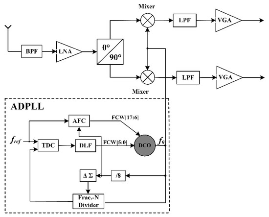
Figure 1.
Block diagram of the quadrature receiver.
2. The Proposed LC-DCO Based on MACK
2.1. Model of the Varactor Tank Based on MACK
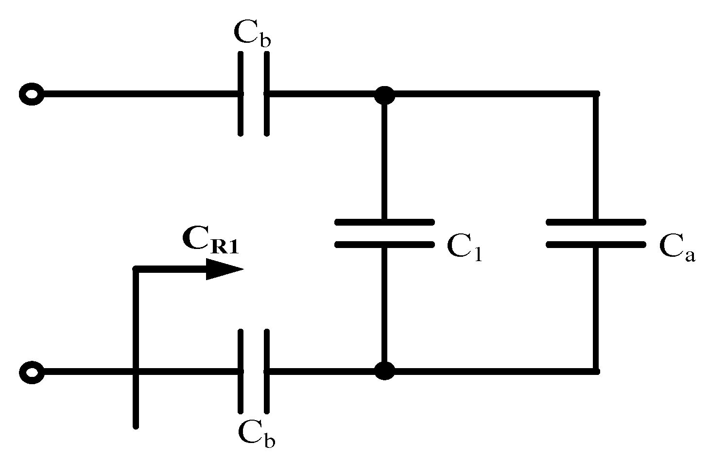
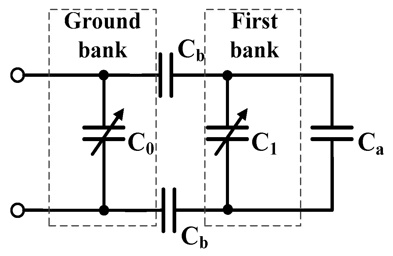
The model of a varactor tank based on one-stage capacitance shrinking is shown in Figure 2. C0 and C1 represent the actual capacitance values of the ground and the first varactor bank, respectively. Ca is the attenuating capacitor and Cb is the bridging capacitor that connects C0 and C1 in series. Thanks to the serial bridging capacitor Cb, the unit variable capacitance of the tank (ΔCfra) is much smaller than that of any varactor bank, which is determined by
where C1M represents the maximum capacitance values of the first varactor bank and ΔCint is the unit variable capacitance of the first varactor bank, i.e., ΔC1. A variable named a1 was used to represent the denominator of the shrinking factor in order to simplify the expression of ΔCfra in MACK models. The unit variable capacitance depends on Cb, C1, and C1M. Because C1 changes between the minimum value and maximum value during the actual operation, ΔCfra is a variable value and the smallest unit variable capacitance is achieved when C1 is equal to C1M. The precondition of Equation (3) is

Figure 2.
Model of the varactor tank based on one-stage capacitance shrinking.
The unit variable capacitance can shrink by reducing the ratio of Cb to (C1 + C1M). The unit variable capacitance of the tank (ΔCfra) can be regarded as a fractional part, while ΔCint corresponds to one least significant bit (LSB), which is very similar to the principle of a ΔΣ-DCO. The advantages of this method are no additional power consumption and no additional quantization noise. Therefore, it is suited to low-power and low-voltage design.
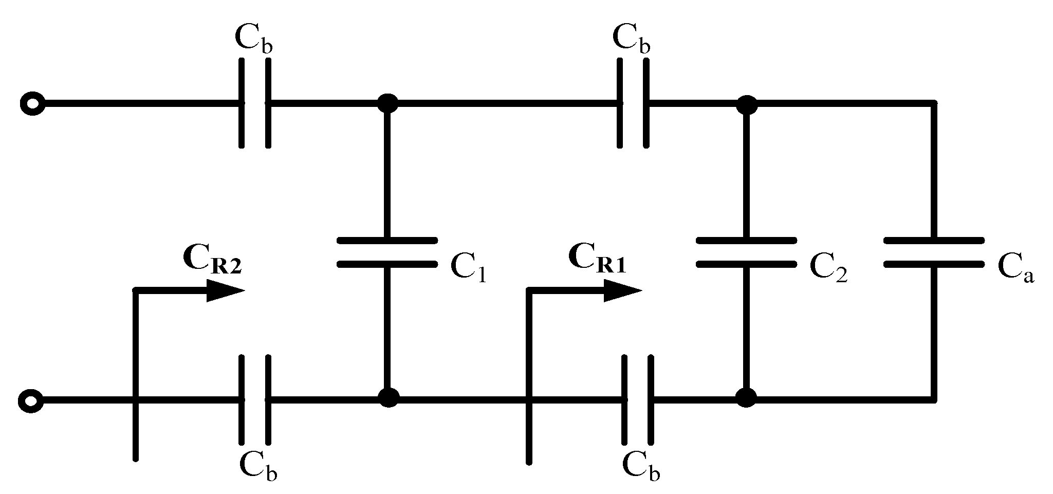
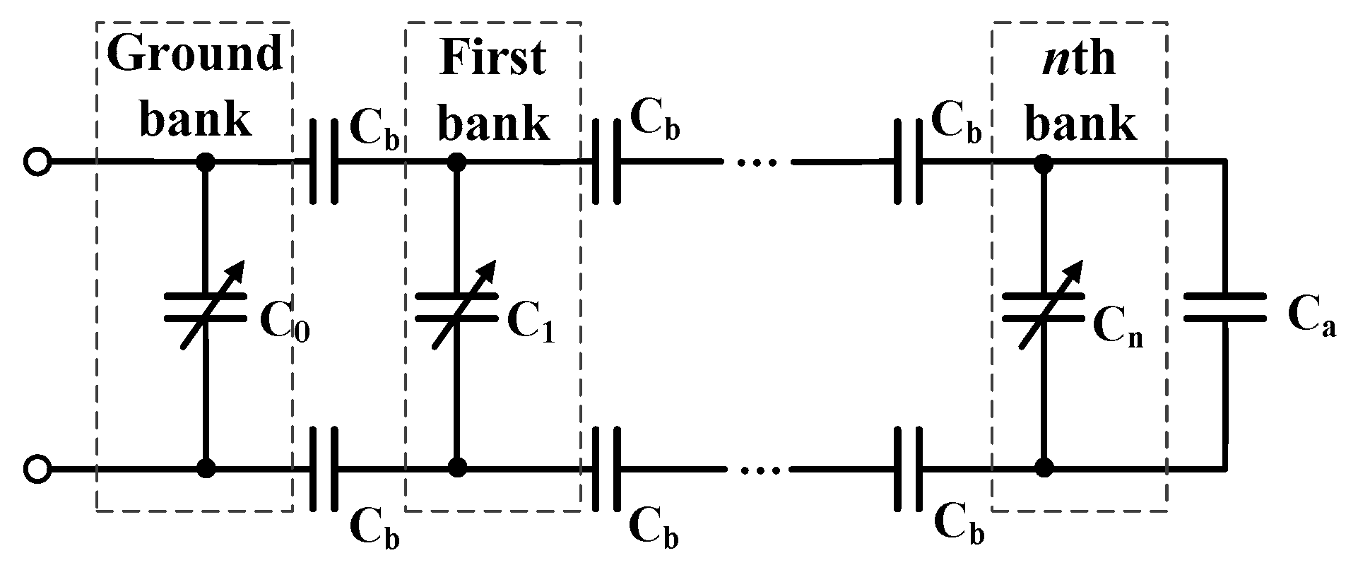
Based on the one-stage model, a MACK technique can achieve a higher-frequency resolution to satisfy more rigorous system requirements. The model was composed of an attenuating capacitor, n pairs of bridging capacitors, and (n + 1) stages of varactor banks, as shown in Figure 3. C0, C1 … Cn represent the actual capacitance values of corresponding varactor banks. The unit variable capacitance of the MACK-based tank is
where every varactor bank has the same maximum capacitance value (CM) and Ci represents the actual capacitance value of the ith stage varactor bank. ΔCint is the unit variable capacitance of the varactor bank in the last stage, i.e., ΔCn. Besides Cb, Ci, and CM, ΔCfra also depends on the stage number of varactor banks. Therefore, the shrinking factor can be very considerable due to the exponential modulation. In order to apply this approach to different applications, a higher- (or lower-) stage MACK-based tank can be easily formed by cascading more (or less) varactor banks, which scarcely increases the power consumption of the chip. The precondition of Equation (5) is
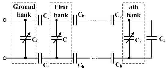
Figure 3.
Model of the varactor tank based on multi-stage capacitance shrinking, in which the bridging capacitors are the same (Cb) and each varactor bank has the same maximum capacitance (CM).
The detailed derivations of Equations (3) and (5) are shown in Appendix A.
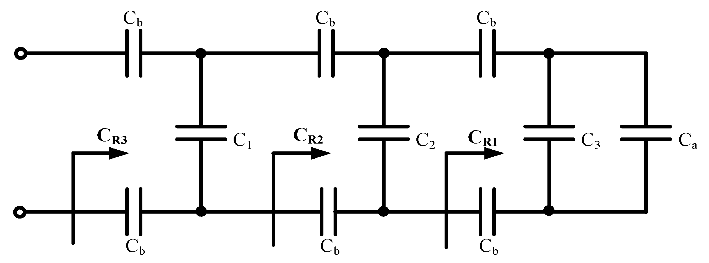
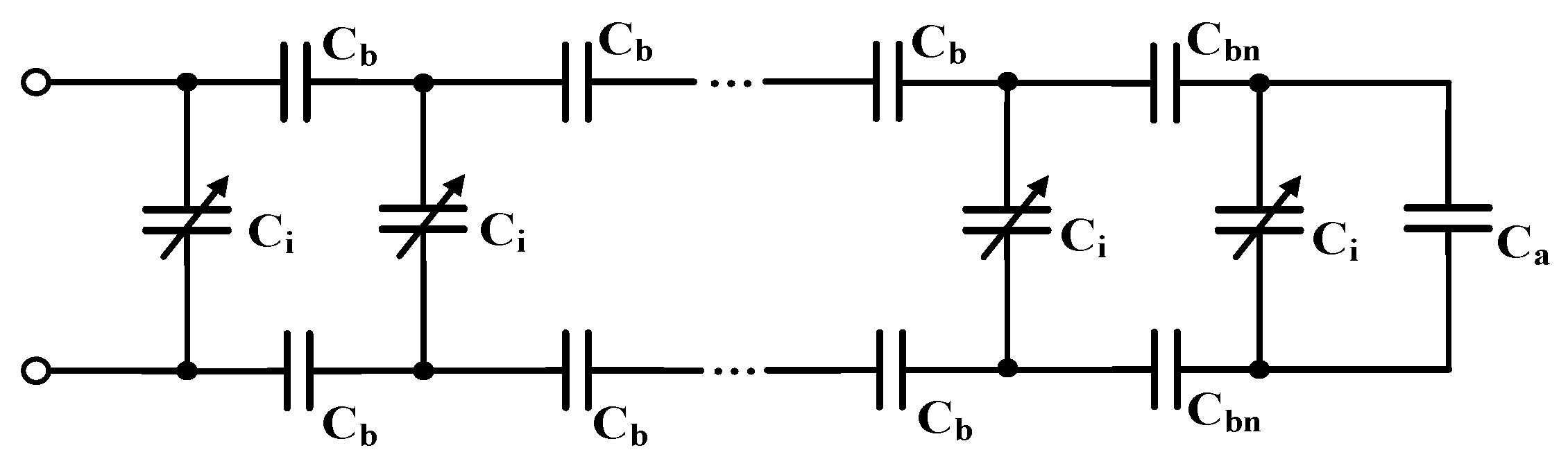
In this work, a smaller bridging capacitor in the last-stage bank was used to improve the resolution, and the model is shown in Figure 4. Each bank had the same maximum capacitance CM. The bridging capacitors in the last-stage bank (Cbn) were smaller than those in the other stages (Cb). Then, the unit variable capacitance is rewritten as
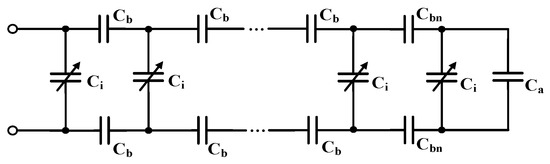
Figure 4.
Model of the varactor tank based on multi-stage capacitance shrinking, in which each varactor bank has the same maximum capacitance (CM) and the bridging capacitors in the last-stage bank (Cbn) are smaller than those in the other stages (Cb).
The precondition of Equation (7) is
The model shown in Figure 4 was used in our test chip. The varactor tank contained three six-bit varactor banks with the same varactor unit in this work. According to the simulation results, the capacitance of the varactor unit ranged from 18 fF to 22 fF. Therefore, ΔCint = 4 fF, and both C1 and C2 ranged from 1134 fF to 1386 fF. Cb = 2 pF and Cbn = 500 fF in this work. Substituting these parameters in Equations (3) and (7), we obtain ΔCfra for different values of n. For n = 1, if a 500-fF bridging capacitor was used, the minimum value and maximum value of ΔCfra were 32.5 aF and 39.3 aF respectively. For n = 2, the relationship between ΔCfra and the actual capacitances (C1 and C2) is shown in Figure 5. The maximum value was about 7 aF when C1 = C2 = 1134 fF, while the minimum value of 4.7 aF was achieved when C1 = C2 = 1386 fF. For n = 3, the maximum value was 0.9 aF when C1 = C2 = C3 = 1134 fF, while the minimum value of 0.5 aF was achieved when C1 = C2 = C3 = 1386 fF. Other cases were similar, in which the maximum value of ΔCfra was achieved when the actual capacitances were the smallest (1134 fF) while the minimum value was achieved when the actual capacitances were the largest (1386 fF). The detailed design of the DCO is demonstrated in the next sub-section.
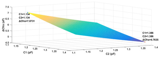
Figure 5.
Relationship between ΔCfra and the actual capacitances (C1 and C2).
2.2. Implementation of the DCO Core
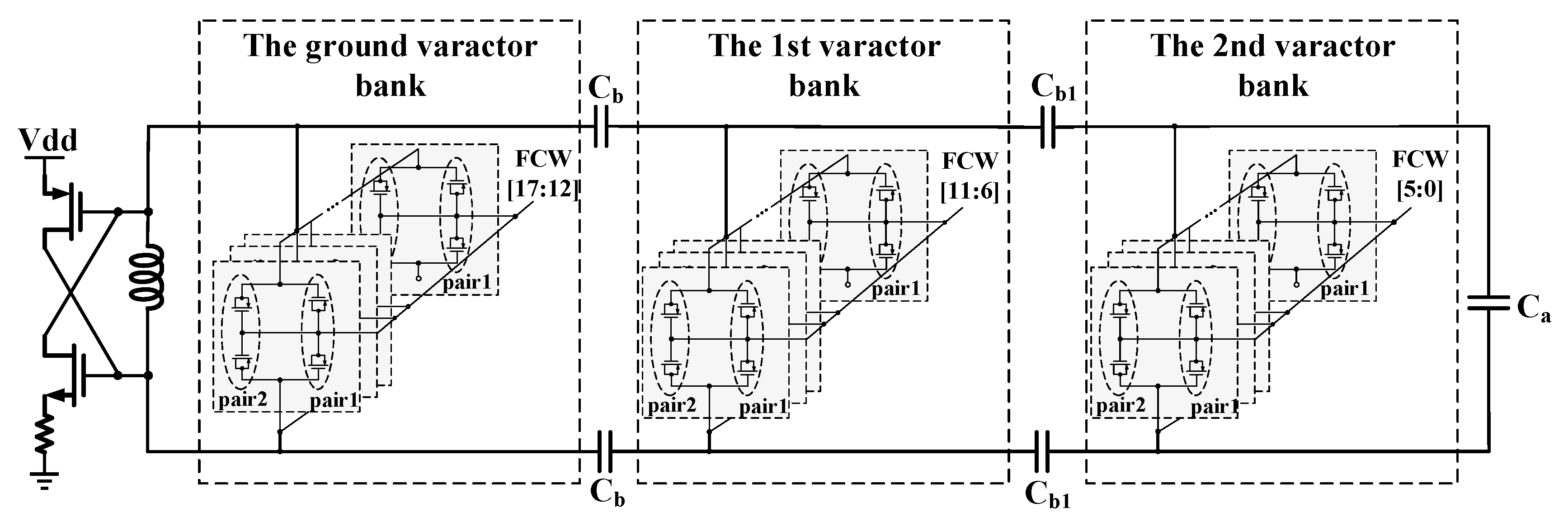
As shown in Figure 6, the LC-DCO core was composed of a cross-coupled MOS pair and an LC tank based on the proposed MACK technique. In order to save the power consumption, a current-reuse structure at a near-threshold supply (0.5~0.7 V) was used. By stacking an NMOS and a PMOS as a cross-coupled pair, the same current from the low-voltage supply flowed into the transistors, which means the current was reused. Therefore, the power was greatly reduced due to both the lower current and lower-voltage supply. In this work, the sizes of the PMOS and the NMOS were 21 μm/130 nm and 10 μm/130 nm respectively, consuming a 1.1-mA current to guarantee oscillation at a 0.6-V supply.
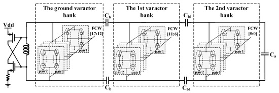
Figure 6.
Structure of the proposed LC-digitally controlled oscillator (DCO).
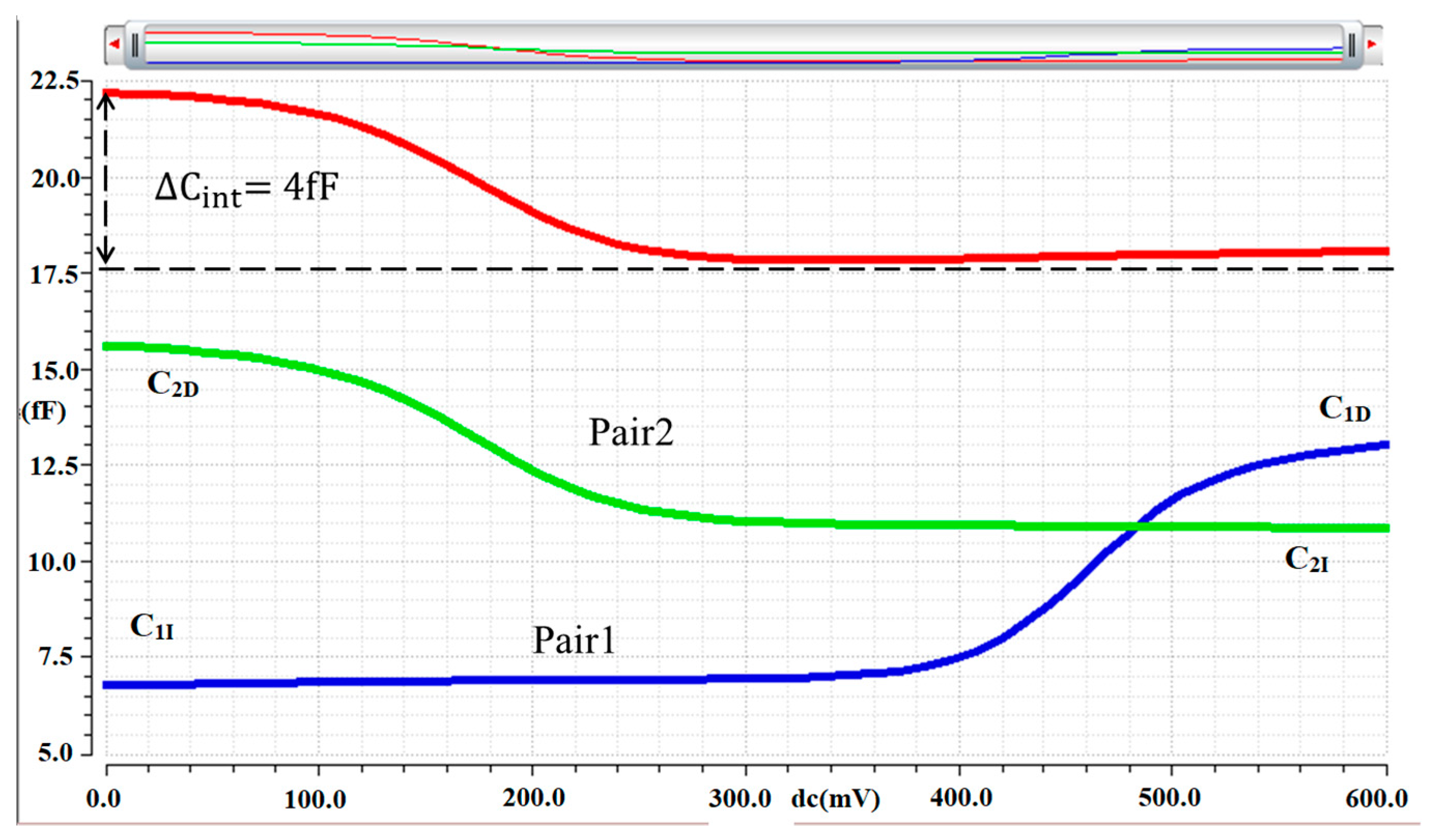
An integrated differential inductor of 2.2 nH with a simulated quality factor of 17 was used in the LC tank. The varactor tank used the model shown in Figure 4, which contained three six-bit varactor banks with the same implementation. An MOS varactor [19], comprising two PMOS pairs that were inversely connected in parallel, was used as the unit of the three varactor banks. When the control signal FCW was high, pair1 worked in the inversion region, while pair2 worked in the depletion region. When FCW was low, pair1 worked in the depletion region, while pair2 worked in the inversion region. The low value of FCW was 0 V, while the high value of FCW was the supply voltage (0.5~0.7 V). The unit variable capacitance equalled (C1I + C2D) − (C2I + C1D), which was smaller than that of every pair, as shown in Figure 7. The size of the transistors in pair1 and pair2 was 8 μm/130 nm and 4 μm/130 nm, respectively, resulting in a 22-fF unit capacitance (CMu) and a 4-fF unit variable capacitance (ΔCint) of a bank. This translated into an integer frequency resolution of about 2 MHz at a carrier frequency of 2.4 GHz.
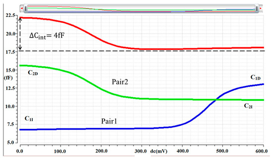
Figure 7.
The C-V curve of the metal oxide superconductor (MOS) varactor.
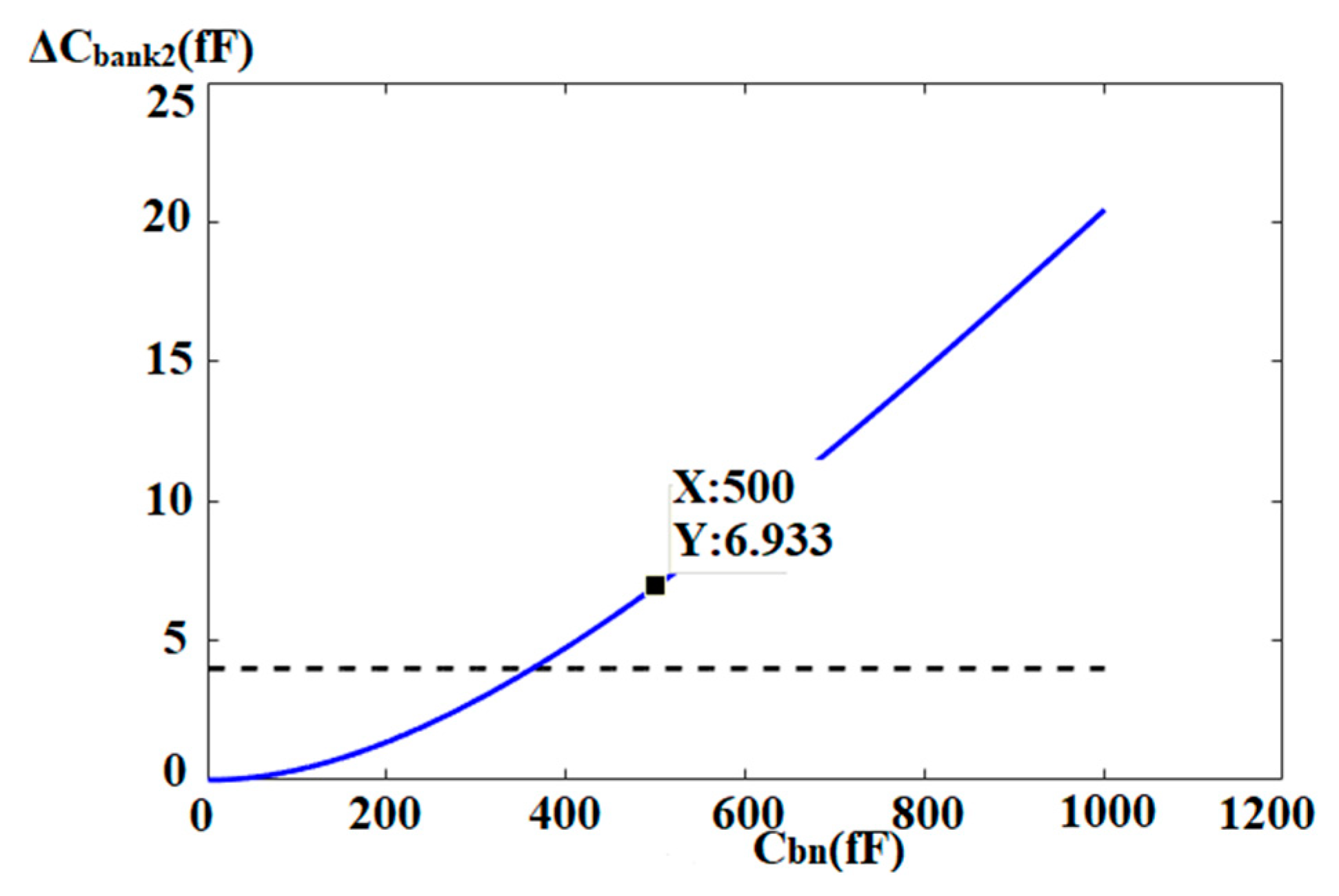
According to Equation (7), when a smaller Cbn was used, a higher resolution was achieved. On the other hand, Cbn should not be extremely small in order to avoid a possible gap at adjacent frequency bands when FCW [5:0] overflows (e.g., FCW [11:0] changes from 000000 111111 to 000001 000000). The relationship between the capacitance range of the second-stage varactor bank (ΔCbank2) and Cbn is plotted in Figure 8. The dashed line in the figure is the bottom line, i.e., ΔCbank2 cannot be smaller than ΔCint. In this work, a 500 fF Cbn was chosen to guarantee sufficient frequency overlap to cope with process, voltage supply, and temperature (PVT) variations. ΔCbank2 approximated 7 fF, which was sufficiently larger than ΔCint. Ca was calculated at approximately 1 pF, according to Equation (8).
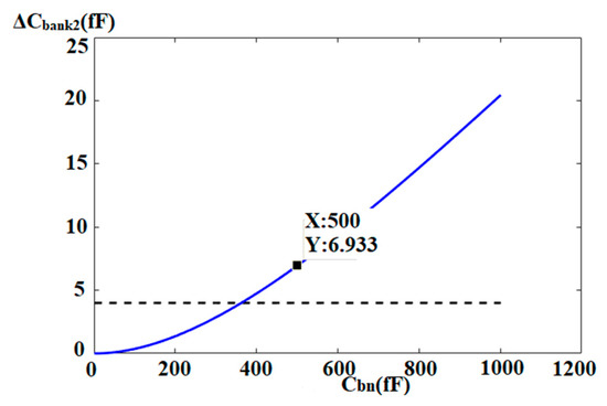
Figure 8.
The relationship between ΔCbank2 and Cbn.
Substituting Cbn = 500 fF, CM = 1386 fF, ΔCint = 4 fF, and n = 2 in Equation (7), we obtained an improved fractional unit variable capacitance (ΔCfra) from 4.7 aF to 7 aF, which corresponds to the maximum actual capacitance (1386 fF) and the minimum actual capacitance (1134 fF). It was impractical to achieve such a small unit variable capacitance by carefully designing the capacitor size only. It was possible to achieve an aF level unit capacitance and a kHz level or even higher-resolution for a DCO with a nine-bit ΔΣ modulator in this case. However, a fast clock, that is, at least one hundred times higher than the reference frequency, was necessary for the ΔΣ modulator to match the high oversampling ratio. This means that a much more power had to be used and it was almost impossible to implement a near-threshold design at such high-frequency with a standard complementary MOS (CMOS) technology. The design parameters used in this work are summarized in Table 1.

Table 1.
Design parameters used in this work.
3. Experimental Results and Discussions
The proposed DCO was designed in the Cadence IC software package and was fabricated using a 130-nm 1P8M CMOS technology. As shown in the Figure 9, the chip occupied 0.9 mm2, including a buffer circuit occupying 0.12 mm2. The shape of the chip was too narrow and the ratio of the length and width was up to 5.7. The chip must accommodate in order to contain many other circuits in the whole block. It affects the DCO performance more or less due to the difficult routing and signal attenuation. It will be improved in the further work.
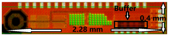
Figure 9.
Chip micrograph.
The proposed DCO core worked at 0.5~0.7-V supplies, while the buffer circuit worked at a 1.2-V supply. The DCO circuit consumed 0.8 mA, 1.1 mA, and 1.7 mA at a supply of 0.5 V, 0.6 V, and 0.7 V, respectively. A 7-mW power was consumed by the buffer circuit used for measurements only.
In this work, the total power was mainly consumed by the output buffer and the cross-coupled pair. The unit MOS varactor was composed of two PMOS pairs that were inversely connected in parallel, as shown in Figure 6. Obviously, the varactor banks scarcely contributed to the power consumption. In order to apply this approach to different applications, a higher- (or lower-) stage MACK-based tank can be easily formed by cascading more (or less) varactor banks to achieve a higher (or lower) resolution, which scarcely increases the power consumption of the chip. However, increasing the stage number will result in a larger chip area and higher production cost.
The frequency range of the DCO is shown in Figure 10a. The DCO had the widest tuning range of 130 MHz when it worked at a 0.5-V supply, ranging from 2.382 GHz to 2.512GHz. The tuning ranges were from 2.385 GHz to 2.5GHz and from 2.385 GHz to 2.494 GHz at a supply of 0.6 V and 0.7 V, respectively.
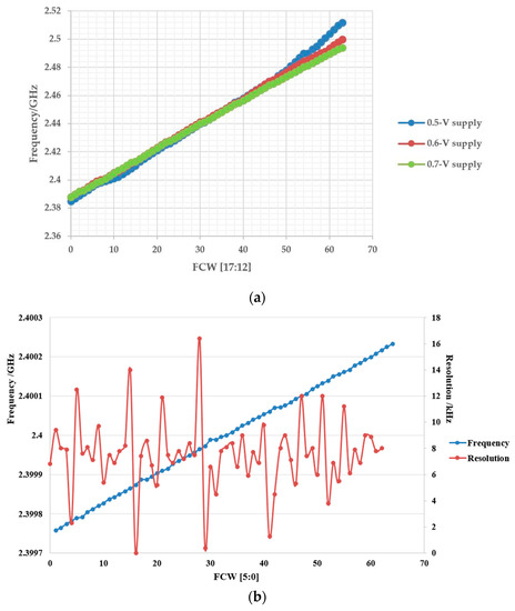
Figure 10.
Frequency range and resolution of the proposed DCO: (a) Frequency range at a 0.5-V~0.7-V supply when FCW [11:6] = FCW [5:0] = 32, and (b) resolution at a 0.6-V supply when FCW [17:12] = 7 and FCW [11:6] = 32.
It is visible that the tuning range narrowed gradually with the rising of the supply. Additionally, the lowest frequencies in the three cases were almost the same, while the highest frequency was inversely proportional to the voltage supply used. The main reason for this is that the three cases had the same control voltage (0 V) when FCW = 0, while the control voltages were different (0.5~0.7 V) when FCW = 1. As shown in Figure 7, the C-V curve (the red line in Figure 7) was not flat in the high-voltage region, where the capacitance became larger as the control voltage rose. Therefore, the capacitance was smallest at a 0.5-V supply (FCW = 0.5 V), while the capacitance was largest at a 0.7-V supply (FCW = 0.7 V). On the other hand, the capacitances were absolutely the same at different supplies when FCW = 0 due to the same control voltage (0 V). Therefore, the frequency range was widest at a 0.5-V supply, while it was narrowest at a 0.7-V supply. All of the three cases covered the frequency range of the Zigbee requirement (2.4 GHz~2.4835 GHz).
Figure 10b shows the results for FCW [5:0], which changed from 0 to 63 at a 0.6-V supply. The average resolution at 2.4 GHz was 7.3 kHz. The step size increased as the frequency rose. The overall average resolution was about 8 kHz. The variations of resolution mainly resulted from the mismatch of varactors. There are two reasons for the mismatch. First, the variations of voltage supply caused the variations of ΔCint through the C-V, characteristic of the MOS varactor. Second, the parasitic capacitance degraded the accuracy of the unit variable capacitance, and the linearity of the resolution was thereby deteriorated.
According to Equation (6), the unit variable capacitance ΔCfra was not a constant when the DCO worked at different frequencies. Therefore, the frequency resolution of the DCO was also a variable value. A lower frequency leads to a smaller ΔCfra and a higher-frequency resolution, which may influence the operation of ADPLL. On power-up, only the auto-frequency calibration (AFC), DCO, and 1/8 divider were active. AFC was used to detect the frequency difference between f0 and the target frequency and changed FCW [17:6] accordingly. FCW [5:0] = 32 and remained constant. The fluctuation of ΔCfra did not disturb frequency locking because the frequency locking did not depend on ΔCfra and ADPLL was a robust negative feedback loop in this step. Once AFC finished frequency locking, it froze FCW [17:6] and activated the time-to-digital converter (TDC), digital loop filter (DLF), and Fractional-N divider. TDC and DLF drove the third-stage bank of DCO, i.e., changed FCW [5:0] to finish phase locking. Because the frequency resolution (or DCO gain) affected the loop gain, bandwidth, and stability of ADPLL, these loop parameters thereby fluctuated when DCO worked at different frequencies. The effect on frequency locking was negligible, but was remarkable on phase locking, especially for the ADPLL with wide tuning range. In order to avoid fluctuations of the loop performance or even fail locking, parameters should be carefully chosen based on the DCO output frequency. A good choice is using a programmable digital loop filter to compensate for the fluctuation of the frequency resolution. When phase locking was finished, FCW [17:6] remained constant, and only FCW [5:0] was variable. Therefore, the range of ΔCfra was limited, although ΔCfra was a variable value according to the analysis in Section 2. For example, when the ADPLL worked at 2.4 GHz, FCW [17:12] = 7 and FCW [11:6] = 32. Therefore, C0 = 1162 fF and C1 = 1262 fF. Assuming that FCW [5:0] had the largest change range, i.e., from 0 to 63, C2 accordingly changed from 1134 fF to 1386 fF (note that the minimum capacitance of the bank is not zero). The calculating ΔCfra changed from 5.1 aF to 6.3 aF, and the range was only 1.2 aF. In fact, the actual change range of ΔCfra was smaller because FCW [5:0] did not change from 0 to 63 when the ADPLL was locked. Therefore, the fluctuation of the frequency resolution was negligible after the ADPLL was locked.
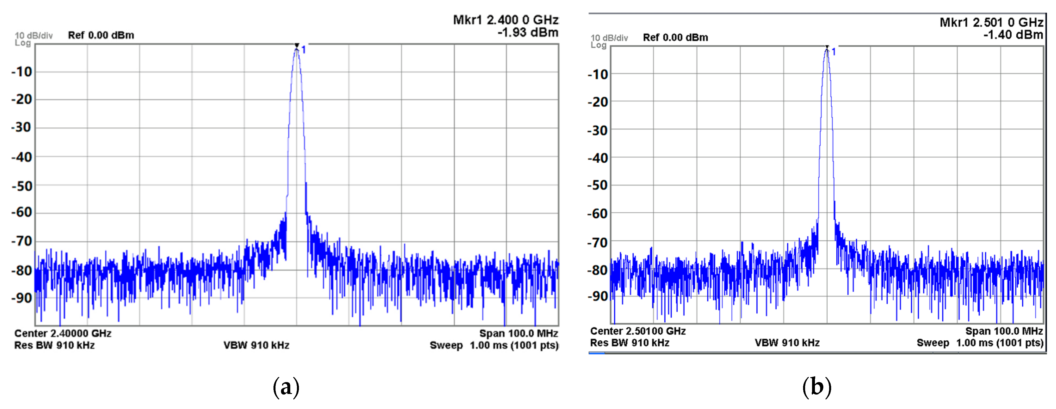
The low- and high-frequency output spectrums are depicted in Figure 11. The output power was −1.93 dBm at 2.4 GHz while it was −1.40 dBm at 2.5 GHz. This translates into a 0.25-V output at 2.4 GHz and a 0.27-V output at 2.5 GHz. The measurements are exhibited at a 0.6-V supply.
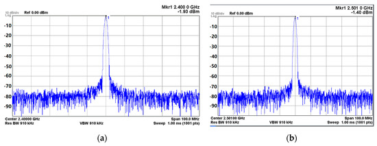
Figure 11.
Output spectrum of the proposed DCO at a 0.6-V supply: (a) When operating at 2.4 GHz, and (b) when operating at 2.5 GHz. Measurements were performed using an Agilent N9020A MXA signal analyzer.
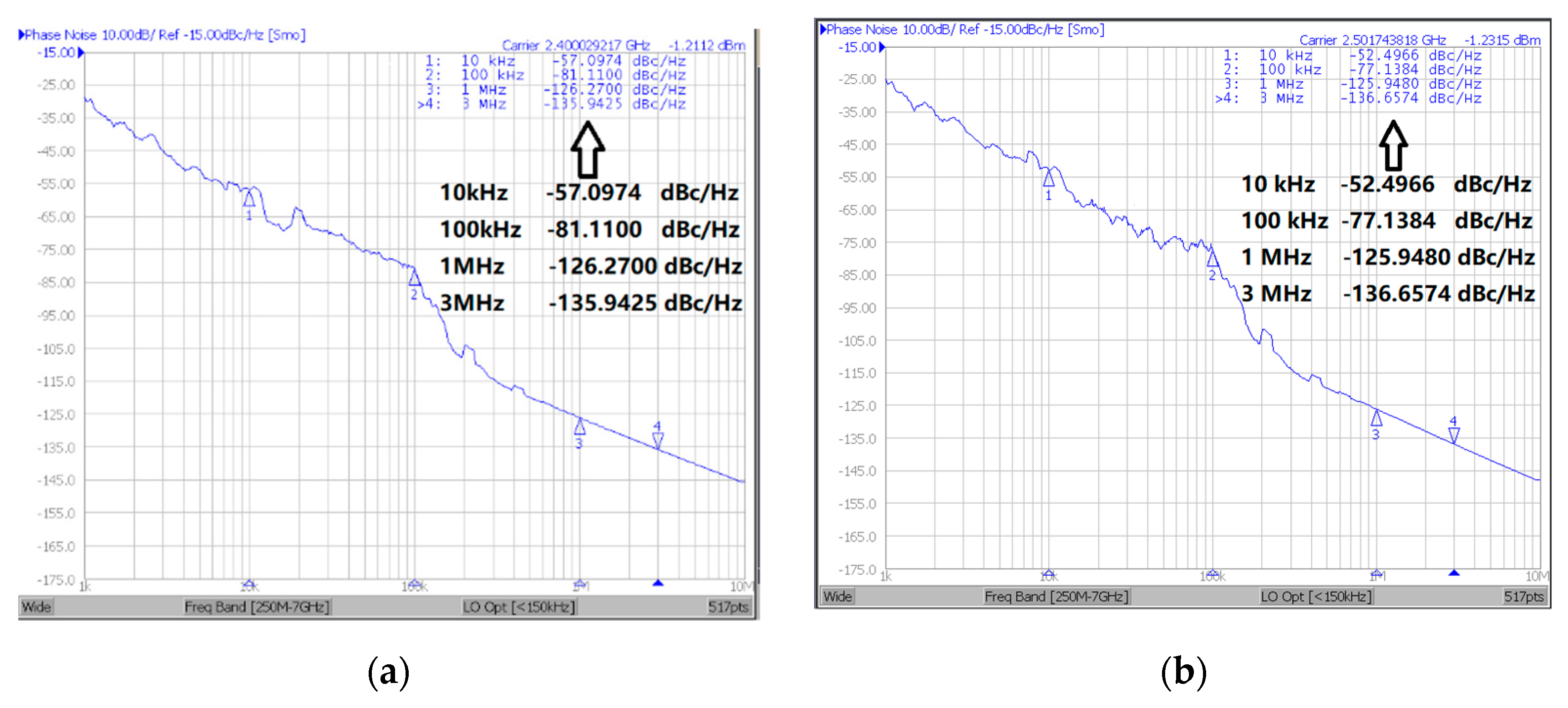
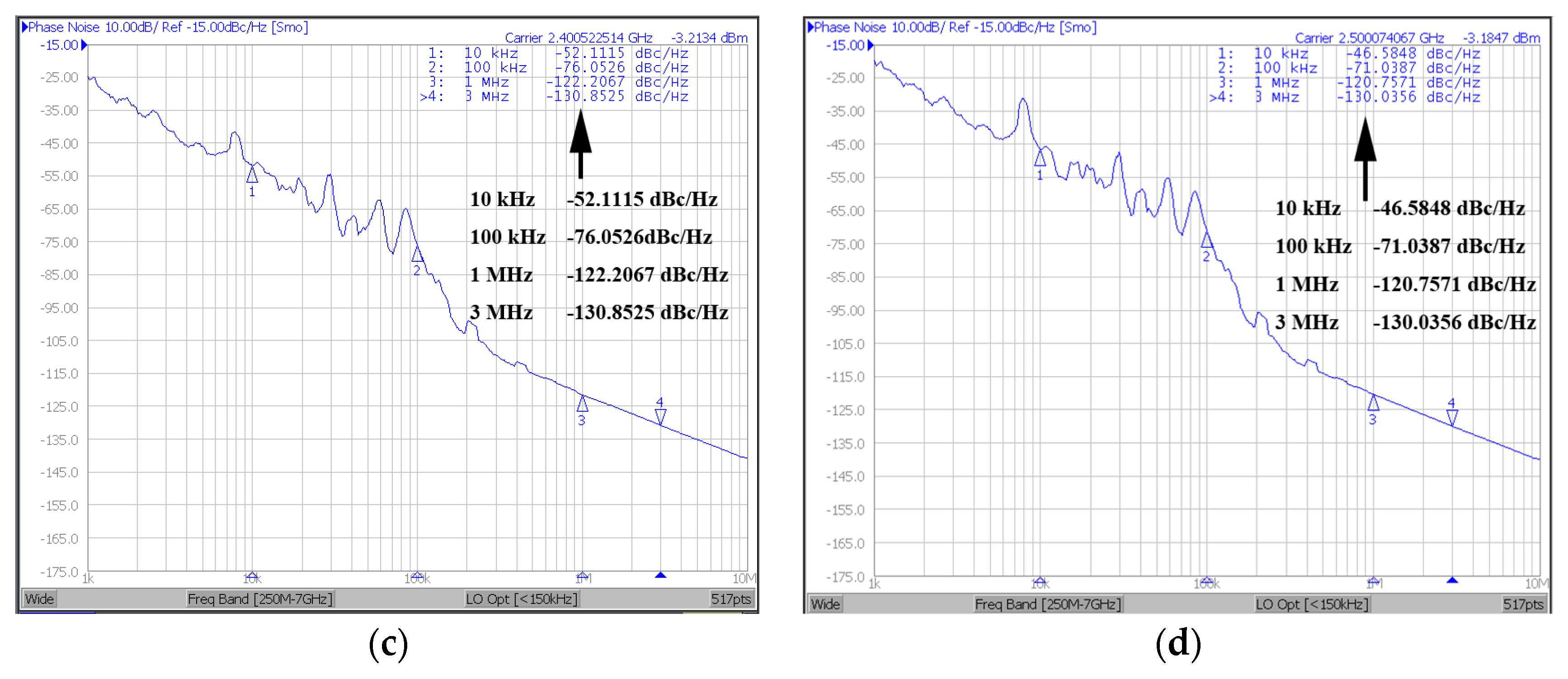
As stated above, the resolution was about 7.3 kHz at a carrier of 2.4 GHz. The resulting phase noise was about −131 dBc/Hz at 1-MHz offset when a 50-MHz reference is used, according to Equation (2). When the DCO works at 2.5 GHz, substituting a 9 kHz resolution into Equation (2), we can obtain −129 dBc/Hz at 1-MHz offset. The measured phase-noise plots of the proposed DCO operating at a low- and high-frequency are shown in Figure 12. As shown in Figure 12a,b (at a 0.6-V supply), at a 2.4-GHz carrier, the measured results were −57.0974 dBc/Hz at 10 kHz offset, −81.11 dBc/Hz at 100 kHz offset, −126.27 dBc/Hz at 1-MHz offset, and −135.9425 dBc/Hz at 3-MHz offset. At a 2.5-GHz carrier, the measured results were −52.4966 dBc/Hz at 10 kHz offset, −77.1384 dBc/Hz at 100 kHz offset, −125.9480 dBc/Hz at 1-MHz offset, and −136.6574 dBc/Hz at 3-MHz offset. The phase noise at a 2.5-GHz carrier was slightly weaker than that at 2.4 GHz, except at 3-MHz offset. As shown in Figure 12c,d (at a 0.5-V supply), at a 2.4-GHz carrier, the measured results were −52.1115 dBc/Hz at 10 kHz offset, −76.0526 dBc/Hz at 100 kHz offset, −122.2067 dBc/Hz at 1-MHz offset, and −130.8525 dBc/Hz at 3-MHz offset. At a 2.5-GHz carrier, the measured results were −46.5848 dBc/Hz at 10 kHz offset, −71.0387 dBc/Hz at 100 kHz offset, −120.7571 dBc/Hz at 1-MHz offset, and −130.0356 dBc/Hz at 3-MHz offset. Compared with the phase noise at a 0.6-V supply, the phase noise at a 0.5-V supply was deteriorated by an average of 5 dB due to the lower current and lower signal amplitude.
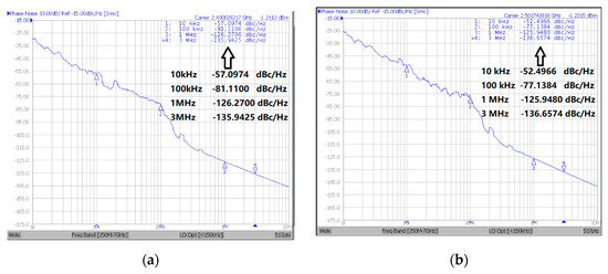
Figure 12.
Phase noise of the proposed DCO (a) when operating at 2.4 GHz at a 0.6-V supply, (b) when operating at 2.5 GHz at a 0.6-V supply, (c) when operating at 2.4 GHz at a 0.5-V supply, and (d) when operating at 2.5 GHz at a 0.5-V supply. Measurements were performed using an Agilent E5052B signal source analyzer.
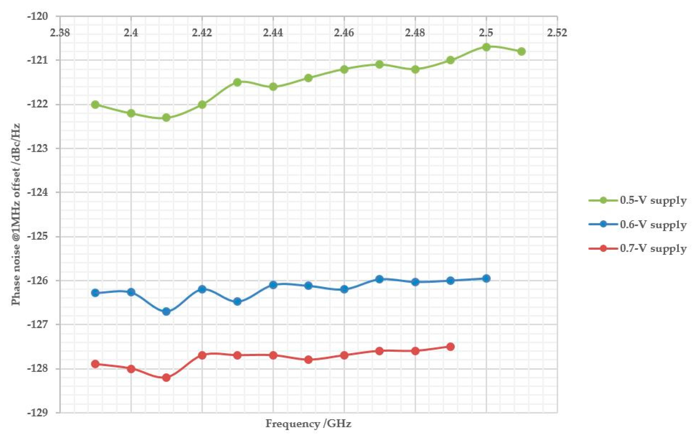
The scatter diagram shown in Figure 13 summarizes the phase noise performance at a 1-MHz offset for the whole tuning range at the supplies of 0.5~0.7 V. The measured results ranged from −122.3 dBc/Hz to −120.7 dBc/Hz, from −126.7 dBc/Hz to −125.95 dBc/Hz and from −128.2 dBc/Hz to −127.5 dBc/Hz at a supply of 0.5 V, 0.6 V, and 0.7 V, respectively. The DCO had the best phase noise performance when VDD = 0.7 V at the cost of the most power, which approximately doubled the consumption when VDD = 0.6 V. Although the power consumption was only 0.4 mW at a 0.5-V supply, the phase noise in this case was greatly deteriorated and the FoM was thereby the worst among the three cases (see below). However, it provides a definite tendency for our future work, in which we will attempt to design circuits at a 0.5-V or even subthreshold supply to further reduce the power on the premise of good phase noise.
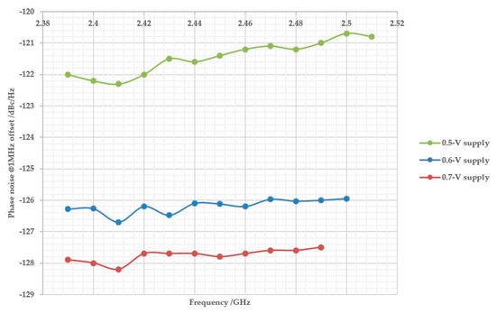
Figure 13.
Phase noise of the proposed DCO in the whole tuning range at a 0.5-V~0.7-V supply.
Table 2 summarizes the performance comparison among similar works. Reference [2] had the lowest supply (0.4 V), widest frequency range (800 MHz), and the highest resolution (1.3 kHz). Reference [8] had the lowest power (only 0.26 mW) and achieved a wider frequency range (470 MHz) than this work, so it achieved the best FoMT, up to 199 dB, among the works in Table 2.
Table 2.
Performance Comparison with Prior Works.
When VDD = 0.6 V, the proposed DCO achieved a phase noise of -126.27 dBc/Hz at a 1-MHz offset at a carrier of 2.4 GHz. The power consumption was 0.66 mW. The calculated FoM was 195.68 dB. The calculated FoM was 193.78dB when VDD = 0.5 V and it was 194.8 dB when VDD = 0.7 V. Among the three supplies (0.5, 0.6, and 0.7 V), the best result was obtained at a 0.6-V supply, which is shown in Table 2.
However, the DCO based on the proposed method improved the FoM at the cost of a narrow frequency range. As shown in Table 2, the frequency range of the proposed DCO was the narrowest (115 MHz) among the other state-of-the-art works (200~800 MHz), which limited the applications of the prototype to a narrowband system. The FoMT was only 189.12dB when VDD = 0.6 V. The frequency range can be widened by increasing more FCWs of every varactor bank. However, the penalty is a larger chip area and higher production cost, although it will not result in higher power in this work. Therefore, a tradeoff between the frequency range and area exists in this work. In addition, properly reducing the frequency overlap between adjacent bands on the premise of no gap is also an option, although it will weaken the tolerance against PVT variations.
4. Conclusions
We proposed a MACK technique for low-voltage and low-power DCOs. The model of the MACK was analyzed based on the analysis of a one-stage model. The unit variable capacitance of the LC tank was largely reduced by the serial bridging capacitor and the increased number of stages (exponential modulation). A particular case and preconditions of each model were also provided to guide the implementation.
The proposed LC-DCO core was designed in Cadence. A current-reuse structure at a near-threshold supply was used for reducing the power. The LC tank based on the MACK technique contained three six-bit varactor banks with the same structure. A MOS varactor, comprising two PMOS pairs that were inversely connected in parallel, was used as the unit of the three banks to achieve a 4-fF ΔCint. All the design parameters and the design flow were provided. A 4.7-aF~7 aF ΔCfra and an 8-kHz resolution were achieved in this work.
Based on the analysis and design, an LC-DCO based on MACK was fabricated in a 130-nm CMOS technology with multiple supplies (0.5~0.7 V for the core, 1.2 V for the buffer). The DCO core consumed 0.4, 0.66, and 1.2 mW at a supply of 0.5, 0.6, and 0.7 V, respectively. The frequency range was from 2.382 GHz to 2.512 GHz at a 0.5-V supply, and the highest frequency was reduced gradually with the rising of the supply. The measured results of phase noise at a 0.6-V supply were −126.27 dBc/Hz at 1 MHz and −125.9480 dBc/Hz at 1 MHz at the carriers of 2.4 GHz and 2.5 GHz, respectively. The best FoM of 195.68 was obtained when VDD = 0.6 V. Thanks to the current-reuse technique, the DCO achieved almost the same noise performance as the traditional cross-coupled structure that theoretically consumes double the current. Furthermore, thanks to the proposed MACK technique, a high resolution was achieved without any additional power consumption. Therefore, the DCO achieved good phase noise and low power simultaneously.
In order to apply this system to different applications, a higher- (or lower-) stage MACK-based tank can be easily formed by cascading more (or less) varactor banks to achieve a higher (or lower) resolution, which scarcely increases the power consumption of the chip. Additionally, the MACK technique can be used not only in LC DCOs, but also in ring oscillators at the cost of the area. The drawback of this work is the narrow frequency range (115 MHz), which limits the applications of the prototype. In future work, the frequency range can be improved by increasing the bits of FCW at the cost of the area or by increasing ΔCint at the cost of a worse resolution and phase noise.
Author Contributions
Conceptualization, Z.W.; formal analysis, H.W. and M.S.; funding acquisition, Z.W.; investigation, X.W.; supervision, Y.G.; writing—original draft, Z.W.; writing—review & editing, S.H. and Z.C.
Funding
This research was funded by the National Natural Science Foundation of China, grant number 61504061 and 61974073.
Acknowledgments
The authors would like to thank Wu Jianping and Liu Xing of Nanjing YUNDONE Electronic Technology for the lab measurement support.
Conflicts of Interest
The authors declare no conflict of interest.
Appendix A
In this appendix, the detailed derivations of Equations (3) and (5) are given as follows.
When n = 1, the simplified model is shown in Figure A1.

Figure A1.
Simplified model of the varactor tank based on one-stage capacitance shrinking.
The total capacitance CR1 is
where C1 represent the actual capacitance values of the first varactor bank and CM is the maximum capacitance values of the first varactor bank.
Therefore, ΔCfra is
where .

Figure A2.
Simplified model of the varactor tank based on two-stage capacitance shrinking.
Therefore, CR2 is
Substituting Equation (A2) in Equation (A3)
Therefore, ΔCfra is
where .

Figure A3.
Simplified model of the varactor tank based on three-stage capacitance shrinking.
When n = 3, the simplified model is shown in Figure A3. According to the analysis above, CR2 is
CR3 is
Substituting Equation (A5) in Equation (A6)
Therefore, ΔCfra is
where .
Equation (A5) can be rewritten as
Similarly, Equation (A7) can be rewritten as
Substituting Equation (A9) in Equation (A7)
According to Equation (A10) and (A11), we can obtain
Therefore, a3 can be expressed as a function of a2 and a1
When n = k (k > 2), the total capacitance can be expressed as
It was assumed that when n = k (k > 2), ΔCfra can be expressed as
where .
When n = k + 1 (k > 2), the total capacitance can be expressed as
and
According to Equation (A12) and (A13), we can obtain
and then
Therefore, when n > 2, we can prove that ΔCfra can be expressed as
where .
In sum, according to Equations (A1), (A4), and (A14), ΔCfra is
References
- Marijan, J.; Romualdas, N. Structure of All-Digital Frequency Synthesiser for IoT and IoV Applications. Electronics 2019, 8, 29. [Google Scholar]
- Li, C.C.; Yuan, M.S.; Chang, C.H.; Lin, Y.T.; Liao, C.C.; Hsieh, K.; Chen, M.; Staszewski, R.B. A 0.2 V Trifilar-Coil DCO with DC-DC Converter in 16 nm FinFET CMOS with 188 dB FOM, 1.3 kHz Resolution, and Frequency Pushing of 38 MHz/V for Energy Harvesting Applications. In Proceedings of the 2017 IEEE International Solid—State Circuits Conference—(ISSCC), San Francisco, CA, USA, 5–9 February 2017; pp. 332–334. [Google Scholar]
- Sasaki, A.; Shinagawa, M.; Ochiai, K. Principles and demonstration of intrabody communication with a sensitive electrooptic sensor. IEEE Trans. Instrum. Meas. 2009, 58, 457–466. [Google Scholar] [CrossRef]
- Sayilir, S.; Loke, W.F.; Lee, J.; Diamond, H.; Epstein, B.; Rhodes, D.L.; Jung, B. A −90 dBm Sensitivity Wireless Transceiver Using VCO-PA-LNA-Switch-Modulator Co-Design for Low Power Insect-Based Wireless Sensor Networks. IEEE J. Solid State Circuits 2014, 49, 996–1006. [Google Scholar] [CrossRef]
- Shirane, A.; Tan, H.; Fang, Y.; Ibe, T.; Ito, H.; Ishihara, N.; Masu, K. A 5.8 GHz RF-Powered Transceiver with a 113 μW 32-QAM Transmitter Employing the IF-based Quadrature Backscattering Technique. In Proceedings of the 2015 IEEE International Solid—State Circuits Conference—(ISSCC), San Francisco, CA, USA, 22–26 February 2015; pp. 248–249. [Google Scholar]
- Akyildiz, I.F.; Su, W.; Sankarasubramaniam, Y.; Cayirci, E. A survey on sensor network. IEEE Commun. Mag. 2002, 40, 102–114. [Google Scholar] [CrossRef]
- Li, C.C.; Yuan, M.S.; Liao, C.C.; Lin, Y.T.; Chang, C.H.; Staszewski, R.B. All-Digital PLL for Bluetooth Low Energy Using 32.768-kHz Reference Clock and ≤0.45-V Supply. IEEE J. Solid State Circuits 2018, 53, 3660–3671. [Google Scholar] [CrossRef]
- Abbasizadeh, H.; Ali, I.; Rikan, B.S.; Lee, D.S.; Pu, Y.; Yoo, S.S.; Lee, M.; Hwang, K.C.; Yang, Y.; Lee, K.Y. 260 µW DCO with Constant Current Over PVT Variations Using FLL and Adjustable LDO. IEEE Trans. Circuits Syst. II 2018, 65, 739–743. [Google Scholar] [CrossRef]
- Naser, P.; Feng, W.K.; Teerachot, S.; Masoud, B.; Staszewski, R.B. A 0.5-V 1.6-mW 2.4-GHz Fractional-N All-Digital PLL for Bluetooth LE With PVT-Insensitive TDC Using Switched-Capacitor Doubler in 28-nm CMOS. IEEE J. Solid State Circuits 2018, 53, 2572–2583. [Google Scholar]
- Bae, J.; Radhapuram, S.; Jo, I.; Kihara, T.; Matsuoka, T. A Design of 0.7-V 400-MHz Digitally-Controlled Oscillator. IEICE Trans. Electron. 2015, 98, 1179–1186. [Google Scholar] [CrossRef]
- Taeho, S.; Young, S.L.; Seyeon, Y.; Jaehyouk, C. A −242 dB FOM and -75dBc-Reference-Spur Ring-DCO-Based All-Digital PLL Using a Fast Phase-Error Correction Technique and a Low-Power Optimal-Threshold TDC. In Proceedings of the 2018 IEEE International Solid—State Circuits Conference—(ISSCC), San Francisco, CA, USA, 11–15 February 2018; pp. 396–398. [Google Scholar]
- Sheng, D.; Chung, C.C.; Lan, J.C.; Lai, H.F. Monotonic and low-power digitally controlled oscillator with portability for SoC applications. Electron. Lett. 2012, 48, 321–323. [Google Scholar] [CrossRef]
- Chien, Y.Y.; Ching, C.C.; Chia, J.Y.; Chen, Y.L. A Low-Power DCO Using Interlaced Hysteresis Delay Cells. IEEE Trans. Circuits Syst. II 2012, 59, 673–677. [Google Scholar]
- Liu, Y.H.; Van Den Heuvel, J.; Kuramochi, T.; Busze, B.; Mateman, P.; Chillara, V.K.; Wang, B.; Staszewski, R.B.; Philips, K. An Ultra-Low Power 1.7–2.7 GHz Fractional-N Sub-Sampling Digital Frequency Synthesizer and Modulator for IoT Applications in 40 nm CMOS. IEEE Trans. Circuits Syst. I 2017, 64, 1094–1105. [Google Scholar] [CrossRef]
- Vytautas, M.; Romualdas, N. Design of High Frequency, Low Phase Noise LC Digitally Controlled Oscillator for 5G Intelligent Transport Systems. Electronics 2019, 8, 72. [Google Scholar]
- Jing, C.Z.; Qing, J.D.; Tad, K. A 3.3 GHz LC-based digitally controlled oscillator with 5kHz frequency resolution. In Proceedings of the 2007 IEEE Asian Solid–State Circuits Conference—(ASSCC), Jeju, Korea, 12–14 November 2018; pp. 428–431. [Google Scholar]
- Shao, H.W.; Jin, G.Q.; Rong, L.; Hao, C.; Hua, Z.Y. A Noise Reduced Digitally Controlled Oscillator Using Complementary Varactor Pairs. In Proceedings of the 2007 IEEE International Symposium on Circuits and Systems—(ISCAS), New Orleans, LA, USA, 27–30 May 2007; pp. 937–940. [Google Scholar]
- Han, J.H.; Cho, S.H. Digitally controlled oscillator with high frequency resolution using novel varactor bank. Electron. Lett. 2008, 44, 1450–1452. [Google Scholar] [CrossRef]
- Wang, Z.; Hu, S.; Cai, Z.; Zhou, B.; Ji, X.; Wang, R.; Guo, Y. A 2.4-GHz All-Digital Phase-Locked Loop with a Pipeline-ΔΣ Time-to-Digital Converter. IEICE Electron. Express 2017, 14, 20170095. [Google Scholar] [CrossRef]
- Staszewski, R.B.; Waheed, K.; Dulger, F.; Eliezer, O.E. Spur-Free Multirate All-Digital PLL for Mobile Phones in 65 nm CMOS. IEEE J. Solid State Circuits 2011, 46, 2904–2919. [Google Scholar] [CrossRef]
- Mohamed, E.; Kamran, E. A Wideband Low-Power LC-DCO-Based Complex Dielectric Spectroscopy System in 0.18 µm CMOS. IEEE Trans. Microw. Theory Tech. 2017, 65, 4461–4474. [Google Scholar]
- Masoud, B.; Staszewski, R.B. A Class-F CMOS Oscillator. IEEE J. Solid State Circuits 2013, 48, 3120–3133. [Google Scholar]
- Yingchieh, H.; Yu, S.Y.; Chia, C.C.; Chauchin, S. A Near-Threshold 480 MHz 78 µW All-Digital PLL With a Bootstrapped DCO. IEEE J. Solid State Circuits 2013, 48, 2805–2814. [Google Scholar]
- Selvakumar, A.; Zargham, M.; Liscidini, A. Sub-mW Current Re-Use Receiver Front-End for Wireless Sensor Network Applications. IEEE J. Solid State Circuits 2015, 50, 2965–2974. [Google Scholar] [CrossRef]


© 2019 by the authors. Licensee MDPI, Basel, Switzerland. This article is an open access article distributed under the terms and conditions of the Creative Commons Attribution (CC BY) license (http://creativecommons.org/licenses/by/4.0/).