Article

A Ruggedness Improved Mobile Radio Frequency Power Amplifier Module with Dynamic Impedance Correction by Software Defined Atomization

1
Wireless Semiconductor Division, Broadcom Inc., Seoul 06771, Korea
2
Department of Electronics Engineering, Korea National University of Transportation, 50 Daehak-ro, Chungju-si, Chungbuk 380-702, Korea
*
Author to whom correspondence should be addressed.
Electronics 2019, 8(11), 1317; https://doi.org/10.3390/electronics8111317
Submission received: 8 October 2019 / Revised: 31 October 2019 / Accepted: 7 November 2019 / Published: 8 November 2019
(This article belongs to the Special Issue New CMOS Devices and Their Applications)

Abstract

:
A ruggedness improved multi-band radio frequency (RF) power amplifier (PA) module applicable to mobile handsets, which are required to survive against a serious load impedance change under extreme power and bias conditions, is presented. In this method, the load impedance of PA is adaptively adjusted with a digitally controlled impedance corrector to keep the PA safe by performing a load mismatch detection. The impedance mismatch detector, impedance corrector, and other RF switches were all integrated into a single integrated circuit (IC) using silicon on insulator (SOI) complementary metal oxide semiconductor (CMOS). For the verification purpose, a 2-stage hetero junction bipolar transistor (HBT) PA module adopting this method was fabricated. At a frequency of 1915 MHz, a collector bias voltage of 4.2 V, and over a wider range of load impedance variation between a VSWR of 1 and a VSWR of 5.5, it did not fail. When this technique was not applied with a voltage standing wave ratio (VSWR) range of 1 to 4, it resulted in an acceptable RF performance degradation of 1% power added efficiency (PAE) in envelope tracking (ET) mode. Moreover, it survived at a bias voltage 1V larger than when the technique was not applied for the same mismatch condition.

1. Introduction

Since the RF PAs in a mobile device are connected to an antenna, they must go through impedance mismatches caused by environmental changes. The PA can be damaged when a load mismatch occurs, therefore the PA’s ruggedness was a main concern for Tx chain in mobile handsets. For this reason, many efforts were made to improve it and solutions for sufficient ruggedness were provided [1,2,3,4,5,6,7,8,9,10,11,12,13], including: Clamping circuit [1,2,3], resistive emitter ballasting [4], closed loop protection technique [1,5,6,7,8,9,10], high voltage process, and so on. A general ruggedness requirement for PA-duplexer (PAD) modules is to have no damage or permanent performance degradation with a full RF input power drive under high load VSWR conditions at a maximum supply voltage. Typical values for the full RF input power, VSWR, and the maximum supply voltage have been 10 dBm, 10:1, and 4.2 V, respectively. However, recent specifications for mobile handsets have changed and the required ruggedness for a mobile RF PA becomes even more challenging for the following reasons:
  • Larger power requirement for High Power User Equipment (HPUE)—Average output power should increase by 3 dB.
  • Signal with higher Peak to Average Power Ratio (PAPR)—Peak output power should increase more than 3 dB.
  • Higher supply voltage—The voltage can be increased more than 5 V with boosting technique.
  • Thermal issues with smaller module size—Effective ruggedness should degrade.
Furthermore, the cause of PA failures can vary and the failure mechanism may differ for each frequency band when one RF PA supports multi-band operation. Therefore, RF PAs need an enhanced universal solution for ruggedness improvements instead of solutions for a certain particular failure issue.
This paper presents a ruggedness improvement method for mobile RF PAs using a dynamic load impedance control technique. Since the technique has been developed based on the fact that RF PA’s ruggedness basically depends on a mismatched load impedance, the approach is very intuitive and can protect an RF PA regardless of its failure mechanism. To demonstrate the feasibility of the proposed approach, a mobile RF PA module has been fabricated and tested employing a control logic.

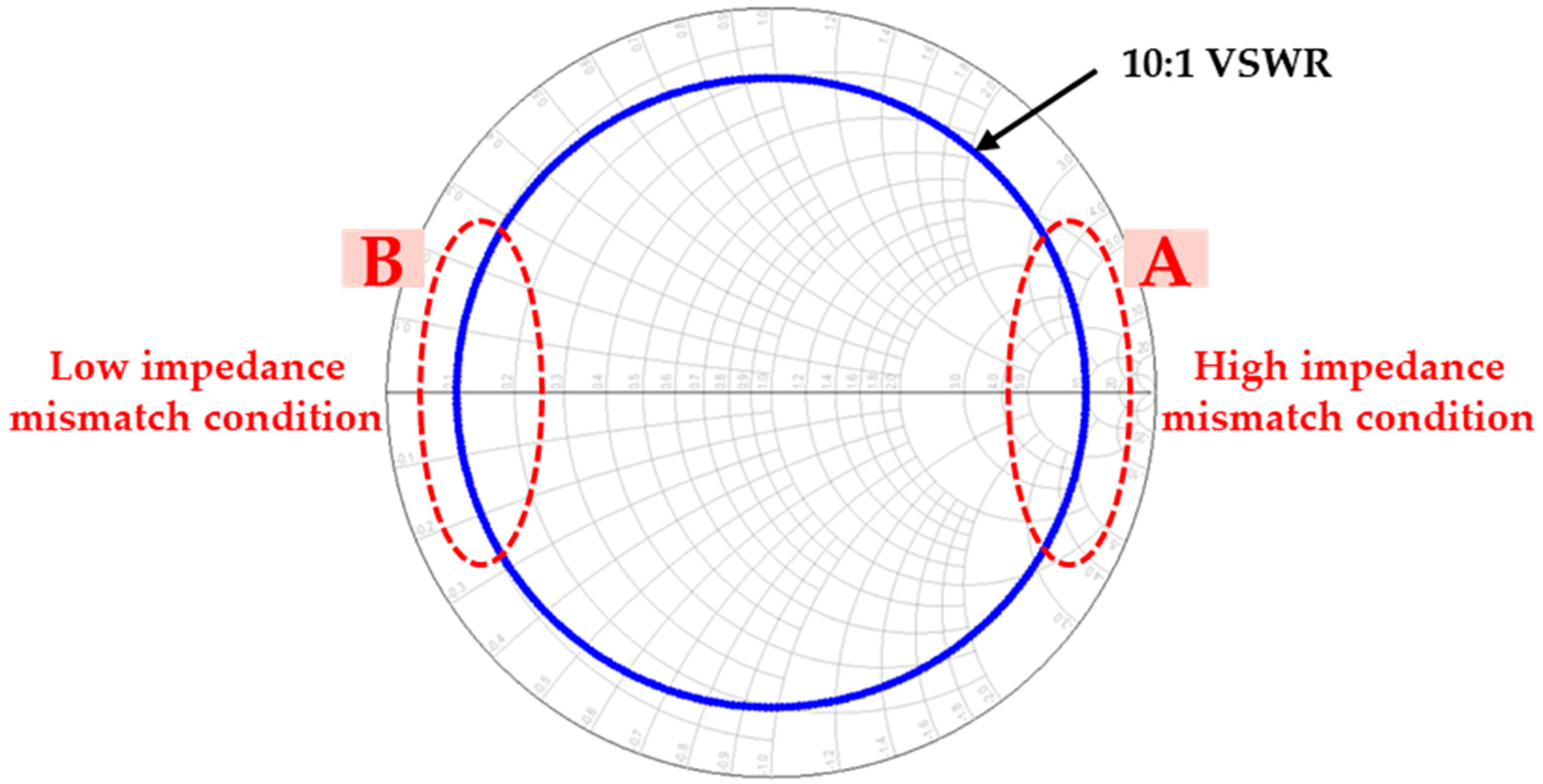
2. The Failure Mechanism in an HBT RF PA under a Mismatch

If a severe impedance mismatch occurs at the antenna port in a mobile device, it leads to a very high VSWR condition. When the mismatched impedance at the antenna port is transformed by PA’s output matching network, the impedance seen by the collector of the HBT in the PA’s final stage can be a high mismatched impedance or a low mismatched impedance depending on the phase of the load. The solid black circle in Figure 1 represents an impedance mismatch with a very large VSWR (10:1) at an antenna port. This condition can lead to PA failure and the failure mechanism varies with the phase of the load, just as the failure mechanisms in region A and B in Figure 1 differ. While the high impedance mismatch condition (region A in Figure 1) results in a very high voltage peak at the collector of the HBT in the final stage, the low impedance mismatch condition (region B in Figure 1) results in a very high current peak.
In an HBT PA, a high collector voltage, which is much larger than the collector to emitter breakdown voltage, with the base open (BVCEO), of a power transistor, had been considered as a main cause of PA failure under a mismatch condition. However, it was revealed that a high collector current, which results in large dissipated power causing a thermal problem, is also a main cause of PA failure [10]. In addition, intermediate impedances located at high VSWR can cause PA failures. Based on these facts, several solutions have been proposed, such as closed-loop protection techniques using collector current sensing circuit [10], as well as clamping circuits [1] and closed-loop technique using a collector voltage sensing circuit [1,3,4,5,6,7,8,9]. However, as the power, voltage, and thermal environments for mobile RF PAs are much more demanding in terms of ruggedness than ever before, there is a need for a more reliable solution. In addition, due to the harsh environment, such as a very dense modular structure, factors that were not previously a problem (e.g., a serious spurious signal) may be a serious PA failure factor, and one PA can have various failure factors. In such cases, the current or voltage measurement methods cannot protect the PA. For example, thermal issue due to large dissipated power (Pdiss) can cause the PA to fail and it is known that Pdiss = Pdc − PRF. Using the detected voltage/current, Pdc can be estimated, but PRF is hard to estimate. Therefore, this kind of method is not able to protect the PA in those cases. On the other hand, since the load impedance is a parameter that directly determines the ruggedness of the PA, sensing and adjusting the load impedance can more clearly determine whether or not the situation will cause PA failure and protect the PA regardless of the cause of the failure than sensing voltage or current.
In order to adjust the load impedance to a safe region for PA protection, it is important to identify the current load impedance, which needs to detect not only load VSWR, but also the load phase. However, since detecting a load phase requires complex analog circuits or digital processors, applying it to a mobile device is not easy. By using load phase detection in a simplified way for detecting areas instead of an accurate value, this work has simplified the detector circuit and made it possible to apply the method to mobile devices.

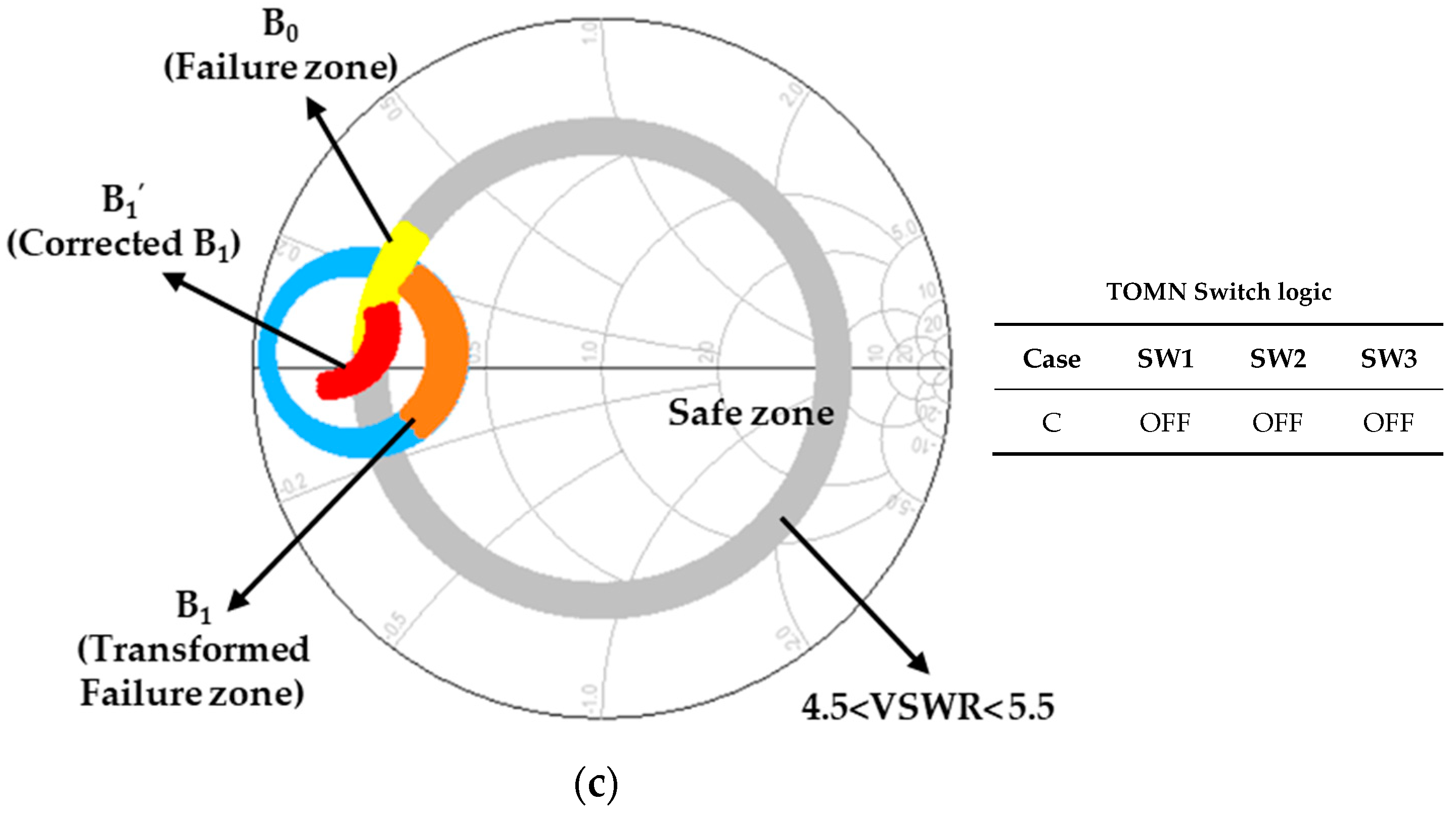
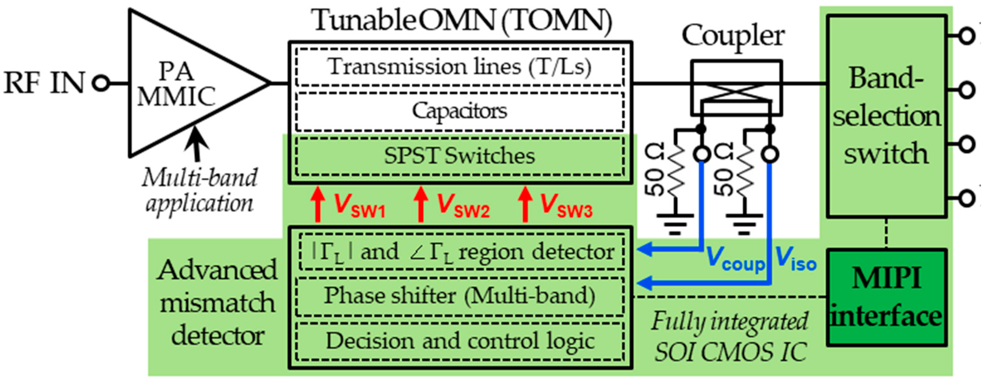
3. Protection by Adaptive Impedance Correction

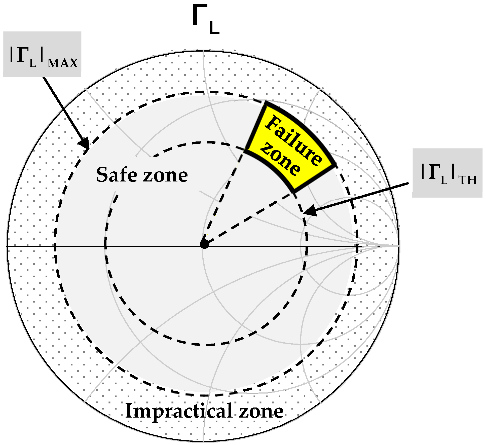
3.1. Operating Principle of Protection

As explained in the previous section, mobile RF PAs fail at certain mismatched load impedances, which depends on PA’s characteristics. Therefore, the load impedance (ΓL) area can be divided into three zones defined by the PA failure, as follows:
  • Failure zone: A PA fails when the load impedance is inside this area.
  • Safe zone: A PA does not fail when the load impedance is inside this area.
  • Impractical zone: It is hard for this impedance region to exist, due to a post-PA loss when the PA output is defined as a reference plane.
Since the failure zone of an RF PA is predetermined by its load-pull characterization, the PA can be readily protected if the load impedance is adjusted inside the safe zone when the load impedance happens to be in the failure zone. For this adaptive impedance adjustment, both detection and correction of load impedance are needed. In both of the authors’ previous works [14,15], a dynamic impedance mismatch detector and corrector were proposed to recover the RF PA’s performance degradation in adjacent channel leakage ratio (ACLR) and PAE, which occur under a mismatch condition.
In this work, the same impedance mismatch detector and corrector which had been reported earlier by us has been utilized here to achieve the intended ruggedness improvement of the RF PAs. With the characterization of an RF PA, its possible load impedance can be divided into two areas: Failure zone and safe zone, as mentioned earlier. The failure zone typically locates at a large VSWR (|ΓL|) and a limited phase (∠ΓL) range as shown in Figure 2. The rest of area can be defined as the safe zone (gray colored area in Figure 2). |ΓL|TH means maximum unconditional safe |ΓL|. For the ΓL, whose magnitude is smaller than the |ΓL|TH, the PA is safe unconditionally, while the PA’s safety depends on the ∠ΓL for the ΓL, whose magnitude is larger than the |ΓL|TH. Although the range of the ∠ΓL and the |ΓL|TH in Figure 2 are determined by the RF PA’s characteristic, the |ΓL|MAX is determined by the loss of post-PA chain (filter, switch, etc.) and its value is generally less than 0.7 (~VSWR of 5.5) because the practical post-PA loss is at least 1.5 dB for recent mobile handsets. Thus, the impedance area where |ΓL|>|ΓL|MAX is impractical and not considered here.
With the knowledge of the predetermined failure zone and safe zone, it is possible to protect the PA by controlling the load impedance using tunable output matching network (TOMN) with the impedance mismatch detector, which determines whether the impedance is in or out of a particular region. For instance, if ΓL is inside the failure zone in Figure 2 then the impedance mismatch detector senses it and informs TOMN to move ΓL into safe zone by a digital control. The proposed ruggedness improved the RF PA configuration, which employs the advanced impedance mismatch detector with a directional coupler and the advanced TOMN, is depicted in Figure 3.

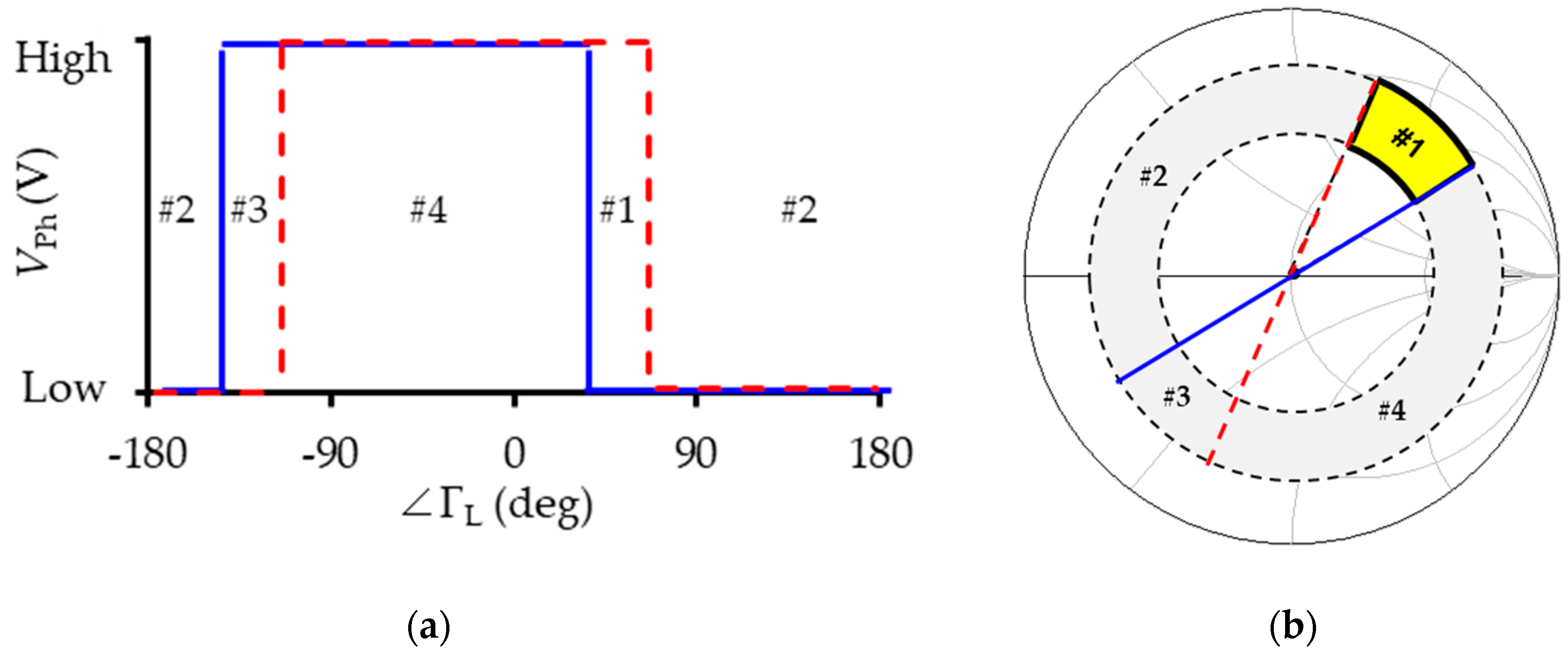
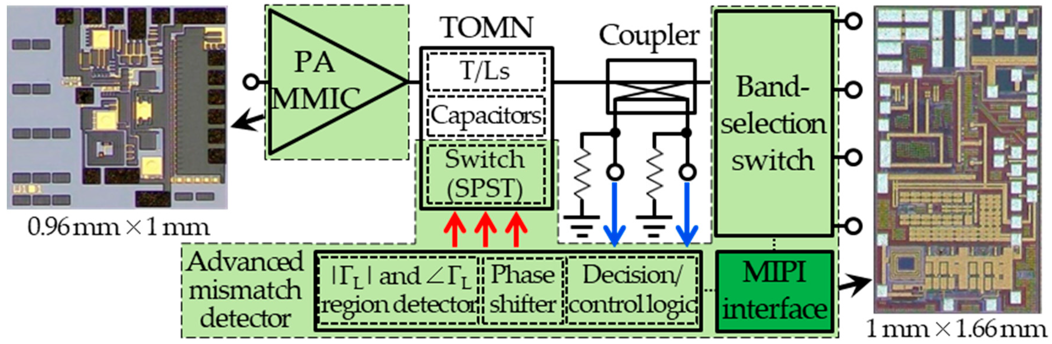
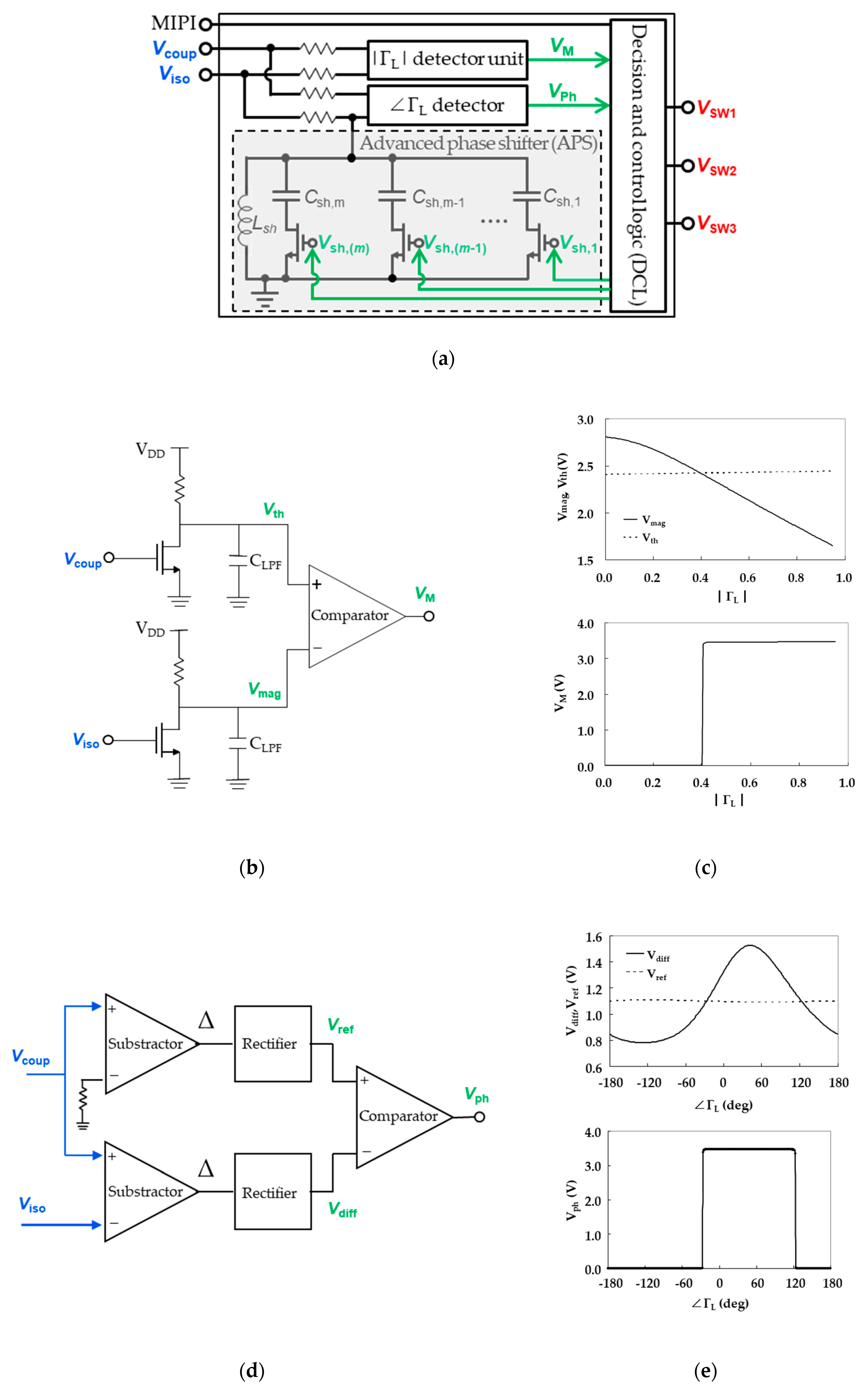
3.2. Impedance Mismatch Detector

The impedance mismatch detector extracts load conditions in terms of the |ΓL| and the ∠ΓL regions to identify whether the PA needs to be protected or not. Figure 4a shows the configuration of the impedance mismatch detector, which is composed of the |ΓL| detector unit, the ∠ΓL detector unit including an advanced phase shifter (APS), and a decision and control logic (DCL) to facilitate mismatch detection.
Figure 4b,d show schematics of a |ΓL| detector and a ∠ΓL detector, respectively. The output voltages of these circuits, VM and Vph, have a ‘High’ or ‘Low’ value depending on the location of ΓL. That is, if the |ΓL| and the ∠ΓL exist in a specific region, they have a ‘High’ value, otherwise they have a ‘Low’ value. Taking Figure 4c,e as an example, in the region where the |ΓL| is greater than 0.4, the VM has a ‘High’ value and in the range where −30° <∠ΓL <30°, Vph has a ‘High’ value. DCL uses a combination of the two results, VM and Vph, to determine if the load impedance is in a certain area.
The APS controls the phase range, where the Vph has ‘High’ value, by adjusting the phase of the Viso applied to the phase detector. The APS consists of a shunt inductor (Lsh) and switched capacitors (Csh,n) controlled by the DCL through a given Vsh. This given control bias (Vsh) is a parallel set ranging from Vsh,0 to Vsh,m. To detect the ∠ΓL region, the DCL applies a given set of Vsh to the APS and stores the accompanied Vph from the ∠ΓL detector unit. The DCL iterates this procedure n times (twice in this work) using another given set of Vsh, after which the current ∠ΓL region is determined by combining the stored n-Vphs. It should be noted that the sets of Vsh values can be adjusted through a MIPI, which makes the detection appropriate for various PA characteristics and multiple operating bands. Table 1 shows a simulation result of a Vsh value set, to define the impedance sections shown in Figure 5b. The total capacitance of the APS used for the first iteration was 1.5pF and for the second iteration, 2pF was used. The phase region where the Vph has a ‘High’ value shows approximately 30 degrees offset between each iteration result, as shown in Figure 5a. After defining the impedance section by designing the |ΓL| and the ∠ΓL detectors, it is possible to determine in which area the ΓL is located according to the result of the Vph value set. Figure 5 shows an example of defining target detection area using the above stated technique. Table 2 describes an example of detecting impedance sections from the Vph value set. In this manner, the impedance sections can be defined as desired by the user through changing the Vsh value set at each time iteration and are changeable through the MIPI control. Then it is used to determine the location of the gamma. The more detailed operating principles of this technique have been previously provided [14,15].

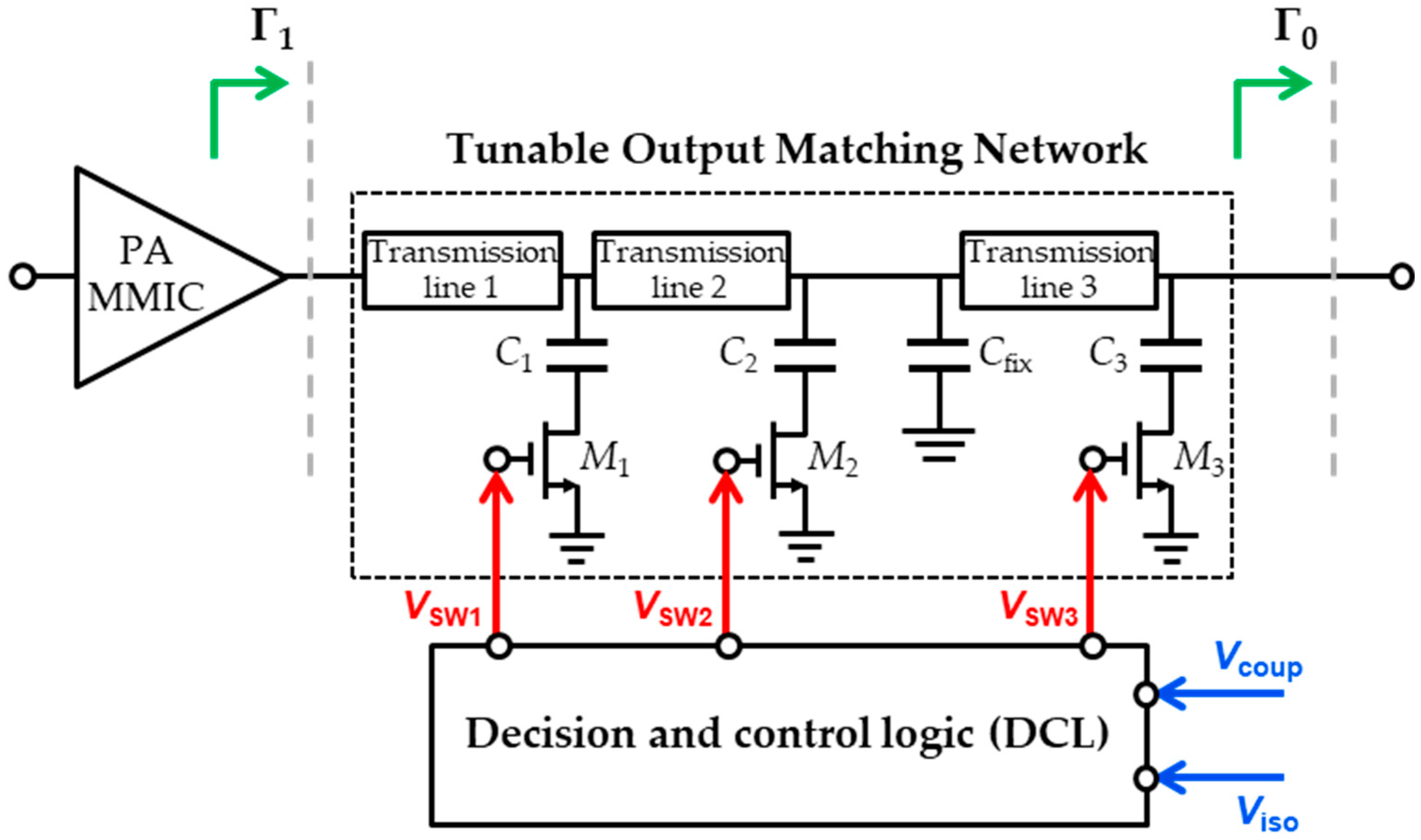
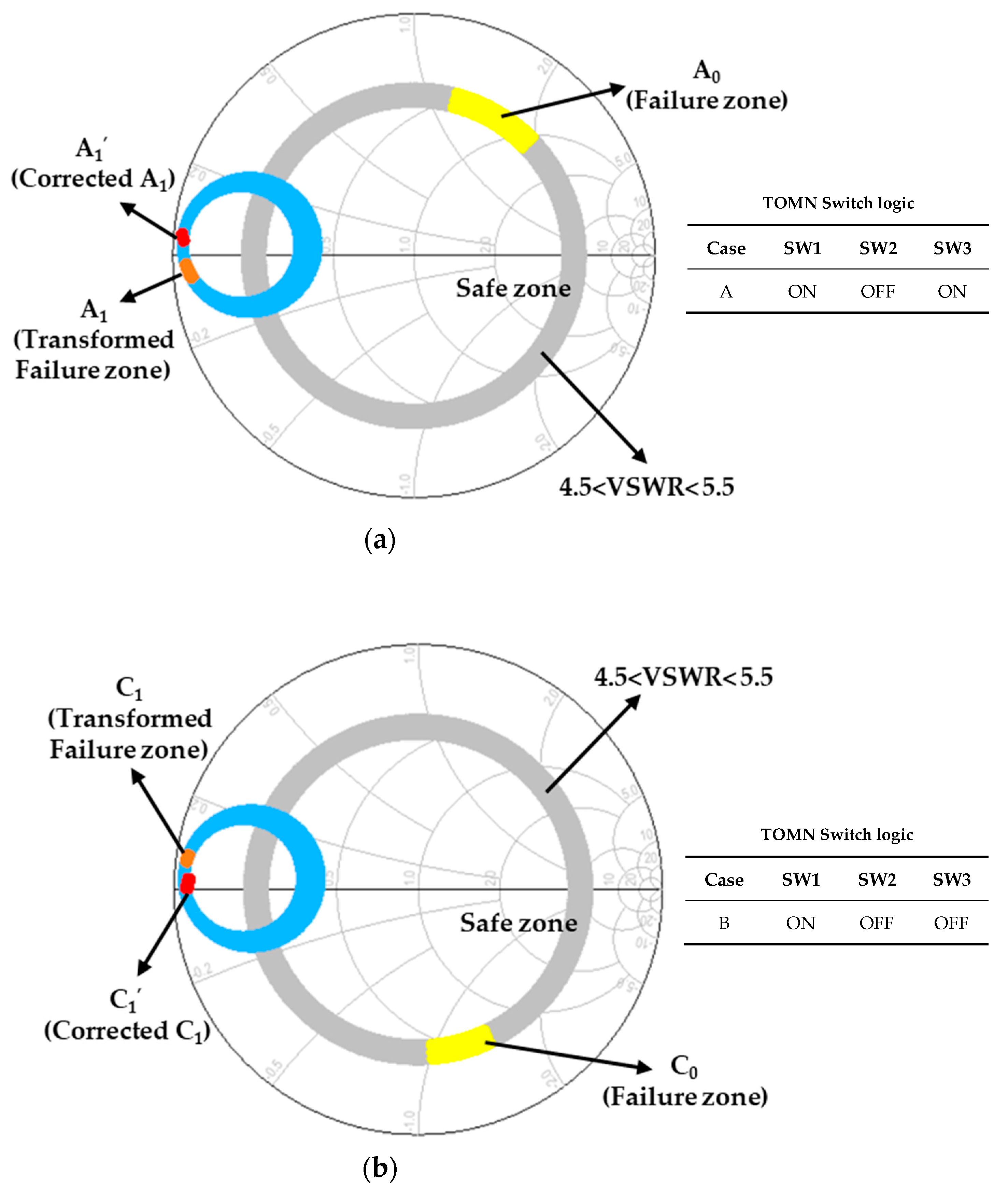
3.3. Dynamic Impedance Corrector

Figure 6 shows the schematic of the impedance corrector using a TOMN. Based on the mismatch detection result, DCL digitally controls the impedance corrector through applying the control voltages to the TOMN. By configuring the capacitance value by the combination of switched capacitors with transmission lines of the TOMN, the impedance adjustment from the failure zone to the safe zone can be achieved for any impedances at which the PA can fail. Considering three cases with different locations for failure zones, for example, Figure 7 shows how each of these impedance corrections are made. In each case, the yellow area (A0, B0, C0) is the failure zone at the antenna port (reference plane Γ0 in Figure 7), the orange area (A1, B1, C1) indicates the failure zone which is transformed by the PA’s output matching network and seen from the collector of the PA final stage (reference plane Γ1 in Figure 7). When the ΓL is located in the yellow region at the antenna port, then the impedance mismatch detector recognizes it and the DCL unit controls the TOMN to protect the PA by moving the impedance at the PA collector out of the orange region to the red area (A1′, B1′, C1′), which is a safe zone.

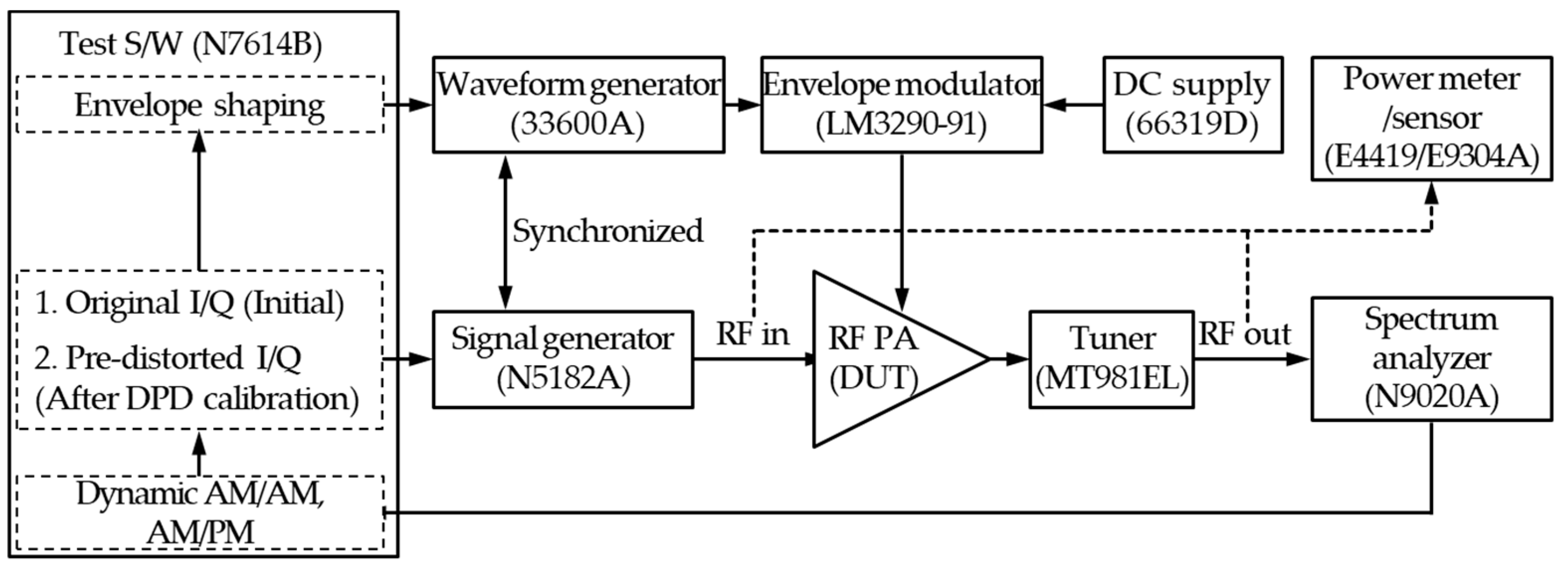
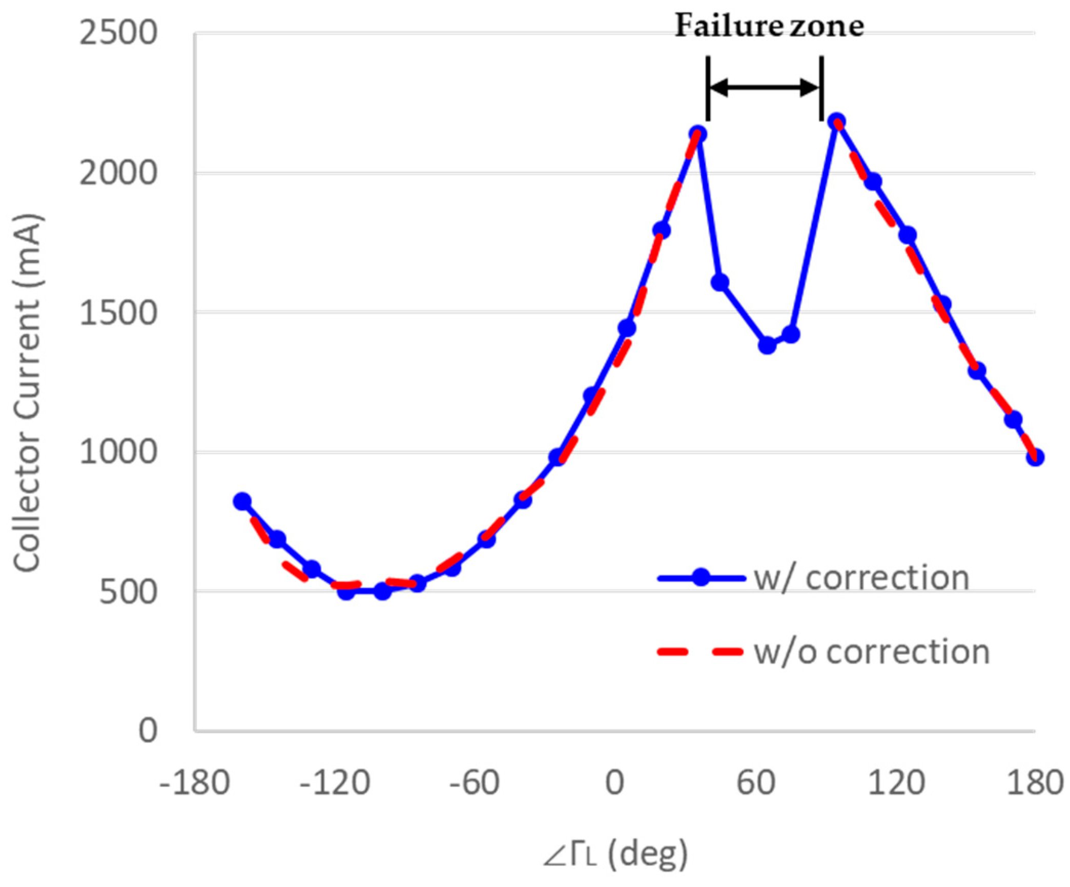
4. Experimental Verification

In order to verify the effectiveness of the proposed protection method, an RF PA module employing the impedance detection and correction technique was fabricated. The PA monolithic microwave integrated circuit (MMIC) was designed as a two-stage amplifier and was fabricated using a 2 μm InGaP/GaAs HBT process. The emitter areas of the first and final stage were 500 and 3600 μm2, respectively. The impedance mismatch detector, the switches of the TOMN, a band-selection switch, and the MIPI interface were all integrated into a single chip using a 0.18 μm SOI CMOS process. Both ICs shown in Figure 8 were mounted on a 400-μm-thick FR4 PCB. The TOMN was implemented using transmission lines on the PCB, off-chip capacitors (C1, C2, C3, and Cfix), and SPST switches (M1, M2, and M3). The TOMN with the off-chip directional coupler (CP0402AE) showed loss of 0.26–0.35 dB, as per the TOMN modes, and the SOI CMOS IC consumed DC power of 25 mW.
To confirm the improvement in ruggedness of a PA module, the measured collector currents were compared with and without the improvement technique using the measurement setup where all instruments were controlled by a dedicated program, as shown in Figure 9. Specific measurement methods and results are described below.
The measurements were performed at a load mismatched condition using a 5 MHz one resource block (RB) long-term evolution (LTE) signal of 10 dBm over collector voltage (Vcc). When the ruggedness improvement technique is deactivated, the PA module showed abnormal current characteristic—a shorted circuit state—over a certain ∠ΓL range (45° < ∠ΓL < 75°) with |ΓL| > 0.64 at a Vcc of 4.2V, which means the module was damaged at the specific ΓL region. This failure zone corresponds to Case A in Figure 7a. With the information of the failure zone, the impedance mismatch detector was set to identify whether ΓL is in this area or not through MIPI; setting |ΓL|TH for the |ΓL| detector as 0.64 and Vshs for the ∠ΓL detector as Table 1. Then impedance corrector was dynamically operated to avoid the failure zone according to the detection result. As a result, the module activating the impedance detection and correction technique showed no abnormal current over the entire ΓL region except the impractical zone, which means the module was not damaged. Figure 10 compares the current measured in two cases: When activating and deactivating the proposed technique, respectively. In Figure 10, the module with correction shows normal collector current values across the entire range, whereas the module without correction does not measure current normally in the particular phase region at the same condition. This result clearly confirms that the proposed technique improves the ruggedness of the PA. The measured ruggedness results over the Vcc at two carrier frequencies (1915/1748 MHz), given in Table 3, to show that this technique is also helpful for a multi-band operation. However, it should be noted that employing this technique has a detrimental effect on the PAE under nominal operating conditions due to the inherent losses of the added components. However, it must be highlighted that envelope tracking mode indicated that this PAE degradation from the loss is of only around 1%, which is acceptable but should be improved in the future.

5. Conclusions

A ruggedness improved multi-band RF PA module that addresses the antenna load impedance mismatch has been presented based on a dynamic impedance detection and correction technique which is digitally controlled through a MIPI. It can more clearly determine whether or not the situation will cause PA failure by tracking the position of the load impedance and also it provides a relatively solid solution for ruggedness improvement by directly tuning load impedance. A two-stage RF PA module for mobile handsets employing this technique was designed and fabricated to demonstrate the improvement in ruggedness. When the ruggedness test was performed at a fixed bias voltage (Vcc) for both Band 1 and Band 3, the PA failure did not occur over the load impedance area up to a VSWR of 5.5. In this case, an acceptable ET PAE degradation of about 1% was measured. For a fixed VSWR condition of 5.5:1, the ruggedness test showed that the PA survived at about a 1 V higher Vcc condition than when this technique was not applied. In this way, the measured results confirm that the RF PAs for mobile handsets can be secured against a much more extreme environment by employing the proposed technique.

Author Contributions

Methodology, validation, paper writing, conceptualization, investigation, J.J. Funding acquisition, supervision, writing—review and editing, M.K.

Funding

This research was supported by the MOTIE (Ministry of Trade, Industry & Energy (10085645) and KSRC (Korea Semiconductor Research Consortium) support program for the development of the future semiconductor device. This research was also supported by Basic Science Research Program through the National Research Foundation of Korea (NRF) funded by the Ministry of Education (2018R1A6A1A03023788), the National R&D Program through the National Research Foundation of Korea (NRF) funded by the Ministry of Science, ICT, and Future Planning (2017M1A7A1A01016265).

Conflicts of Interest

The authors declare no conflict of interest.

References

  1. Yamamoto, K.; Suzuki, S.; Mori, K.; Asada, T.; Okuda, T.; Inoue, A.; Miura, T.; Chomei, K.; Hattori, R.; Yamanouchi, M.; et al. A 3.2-V operation single-chip dual-band Al-GaAs/GaAs HBT MMIC power amplifier with active feedback circuit technique. IEEE J. Solid State Circuits 2000, 35, 1109–1120. [Google Scholar] [CrossRef]
  2. Luo, X.; Halder, S.; Hwang, J. Rugged HBT Class-C power amplifiers with base-emitter clamping. In Proceedings of the 2011 IEEE MTT-S International Microwave Symposium, Baltimore, MD, USA, 5–10 June 2011. [Google Scholar]
  3. King, J. High VSWR Mismatch Output Stage. U.S. Patent 6,137,366, 24 October 2000. [Google Scholar]
  4. Scuderi, A.; Scuderi, A.; Carrara, F.; Palmisano, G. A VSWR-rugged silicon bipolar RF power amplifier. In Proceedings of the Bipolar/BiCMOS Circuits Technology Meeting, Santa Barbara, CA, USA, 9–11 October 2005; pp. 116–119. [Google Scholar]
  5. Bezooijen, A.; Straten, F.V.; Mahmoudi, R.; Roermund, A.H.M.V. Power amplifier protection by adaptive output power control. IEEE J. Solid State Circuits 2007, 42, 1834–1841. [Google Scholar] [CrossRef]
  6. Shin, H.; Ju, H.; Chang, M.F.; Nellis, K.; Zampardi, P. An output VSWR protection Circuit using collector/emitter avalanche breakdown for SiGe HBT power amplifiers. IEICE Trans. Electron. 2004, 87, 1643–1645. [Google Scholar]
  7. Scuderi, A.; La Paglia, L.; Scuderi, A.; Carrara, F.; Palmisano, G. A VSWR-protected silicon bipolar RF power amplifier with soft-slope power control. IEEE J. Solid State Circuits 2005, 40, 611–621. [Google Scholar] [CrossRef]
  8. Bent, G.; Wanum, M.; Hek, A.; Graaf, M.; Vliet, F. Protection circuit for high power amplifiers operating under mismatch conditions. In Proceedings of the 2007 European Microwave Integrated Circuit Conference, Munich, Germany, 8–10 October 2007; pp. 158–161. [Google Scholar]
  9. Ferretti, J.; Preis, S.; Heinrich, W.; Bengtsson, O. VSWR protection of power amplifiers using BST components. In Proceedings of the 2016 German Microwave Conference, Bochum, Germany, 14–16 March 2016; pp. 445–448. [Google Scholar]
  10. Karoui, W.; Parra, T. A protection circuit for HBT RF power amplifier under load mismatch conditions. In Proceedings of the 2008 Joint 6th International IEEE Northeast Workshop on Circuits and Systems and TAISA Conference, Montreal, QC, Canada, 22–25 June 2008; pp. 241–244. [Google Scholar]
  11. Heijningen, M.; Bent, G.; Houwen, E.H.; Chowdhary, A.; Vliet, F.E. L-band AlGaN/GaN power amplifier with protection against load mismatch. In Proceedings of the 2013 European Microwave Conference, Nuremberg, Germany, 6–10 October 2013; pp. 408–411. [Google Scholar]
  12. Heijningen, M.; Bent, G.; Houwen, E.; Chowdhary, A.; Vliet, F.E. VSWR-protected 90 W L-band AlGaN/GaN power amplifier. In Proceedings of the 2014 IEEE MTT-S International Microwave Symposium (IMS2014), Tampa, FL, USA, 1–6 June 2014; pp. 1–3. [Google Scholar]
  13. Sinha, S.; Rao, C.V.N.; Pujara, D. Balanced Power amplifier protection against load mismatch. IEEE Microw. Wirel. Compon. Lett. 2018, 28, 165–167. [Google Scholar] [CrossRef]
  14. Ji, D.; Jeon, J.; Kim, J. A Novel Load Mismatch Detection and Correction Technique for 3G/4G Load Insensitive Power Amplifier Application. IEEE Trans. Microw. Theory Tech. 2015, 63, 1530–1543. [Google Scholar] [CrossRef]
  15. Ji, D.; Jeon, J.; Kim, J. A linearity-improved multiband envelope tracking Tx power amplifier under antenna mismatch for mobile applications. Microw. Opt. Technol. Lett. 2018, 60, 2320–2325. [Google Scholar] [CrossRef]
Figure 1. Cases of a severe impedance mismatch at the antenna port, which can cause a PA failure.
Electronics 08 01317 g001
Figure 2. An example of a typical failure impedance zone where a PA can be damaged. (The phase reference point depends on the position of the impedance mismatch detector).
Electronics 08 01317 g002
Figure 3. The proposed ruggedness improved RF PA module configuration.
Electronics 08 01317 g003
Figure 4. (a) The configuration of the proposed impedance mismatch detector; (b) a schematic of the |ΓL| detector; (c) a simulation of the results of the Vth (threshold voltage), Vmag (magnitude voltage), and VM (magnitude detection voltage) in Figure 4b; (d) a schematic of the ∠ΓL detector; and (e) the simulation results of the Vdiff (difference voltage), Vref (reference voltage), and Vph (phase detection voltage) in Figure 4d.
Electronics 08 01317 g004
Figure 5. An example of defining impedance sections. (a) A simulation result of the Vph with a predetermined Vsh set and (b) the resultant impedance sections.
Electronics 08 01317 g005
Figure 6. A schematic of the impedance corrector using a TOMN controlled by a DCL.
Electronics 08 01317 g006
Figure 7. Examples of an impedance correction with several positions of failure zone (yellow/orange) and corrected impedance (red). (a) Case A (Failure zone: 4.5 < VSWR < 5.5 and 45° < ∠ΓL < 75°); (b) Case B (Failure zone: 4.5 < VSWR < 5.5 and -85° < ∠ΓL < −60°); and (c) Case C (Failure zone: 4.5 < VSWR < 5.5 and 145° < ∠ΓL < 175°).
Electronics 08 01317 g007aElectronics 08 01317 g007b
Figure 8. Photographs of the fabricated PA IC (HBT) and the SOI CMOS IC.
Electronics 08 01317 g008
Figure 9. A measurement setup for the RF characterization under a mismatch. Once the test software (S/W) obtains the information of amplitude modulation (AM) and phase modulation (PM) from the spectrum analyzer, it can provide an envelope shaping function using pre-distorted in-phase (I)/quadrature (Q) data from the digital pre-distorter (DPD) for the ET mode.
Electronics 08 01317 g009
Figure 10. The measured collector current comparison in two cases: ‘With correction using the proposed technique’ and ‘without correction’, to check if the PA is damaged. (frequency = 1915 MHz, Vcc = 4.2 V, |ΓL| = 0.7).
Electronics 08 01317 g010
Table 1. An example of a simulated Vsh set for defining impedance sections as Figure 5a.
Iteration (n = 2)Vsh,5Vsh,4Vsh,3Vsh,2Vsh,1
1st ( )LHHLL
2nd ( ---- )HLLLL
Table 2. An example of detecting an impedance section from the Vph value set. (Figure 5b).
IndexVph (1st)Vph (2nd) Detected section 1
1LH#1
2LL#2
3HH#3
4HH#4
1 Assuming that the |ΓL| is determined from the VSWR detector.
Table 3. A measured ruggedness comparison (|ΓL| = 0.7).
Frequency [MHz]Supply Voltage [V]w/o Impedance Correction w/ Impedance Correction
19153.4PassedPassed
19153.8PassedPassed
19154.2FailedPassed
19155.6-Failed
17483.8PassedPassed
17484.2PassedPassed
17484.6FailedPassed
17485.6-Failed

