Hall-Effect Current Sensors Susceptibility to EMI: Experimental Study


Abstract
:1. Introduction
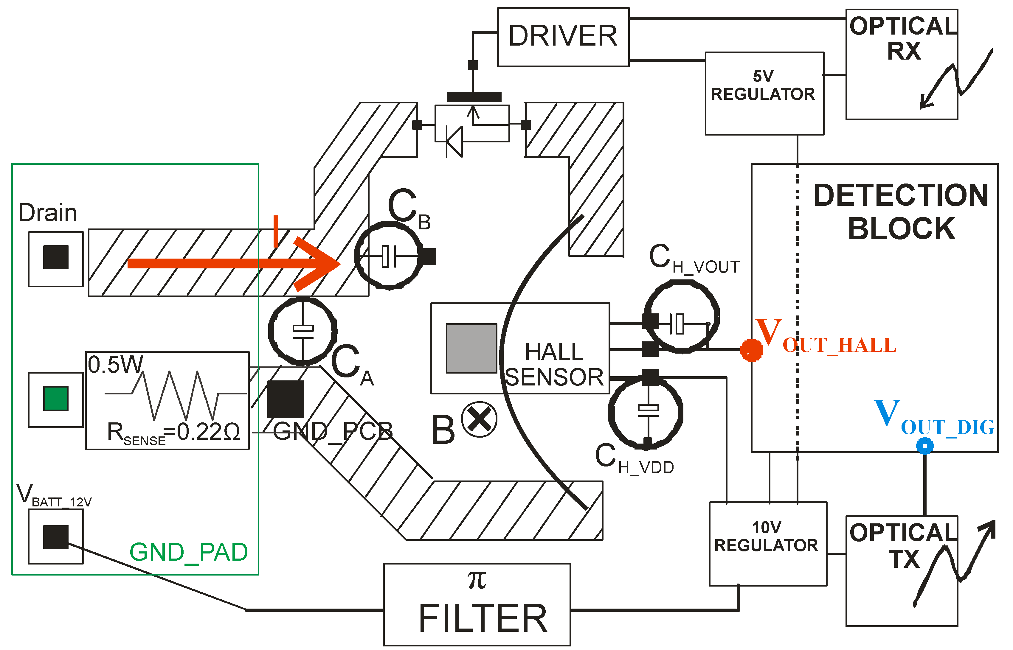
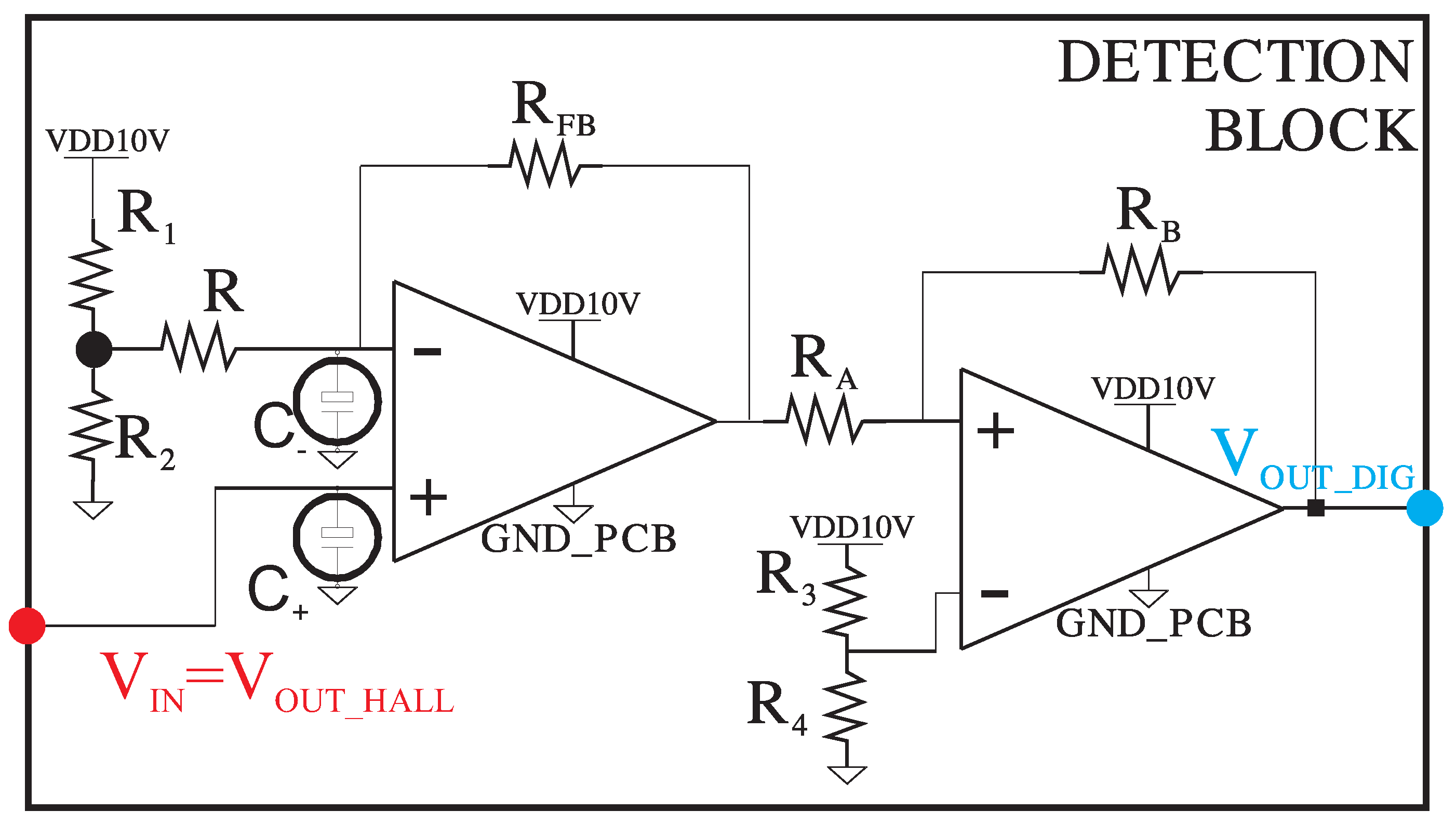
2. Test Board
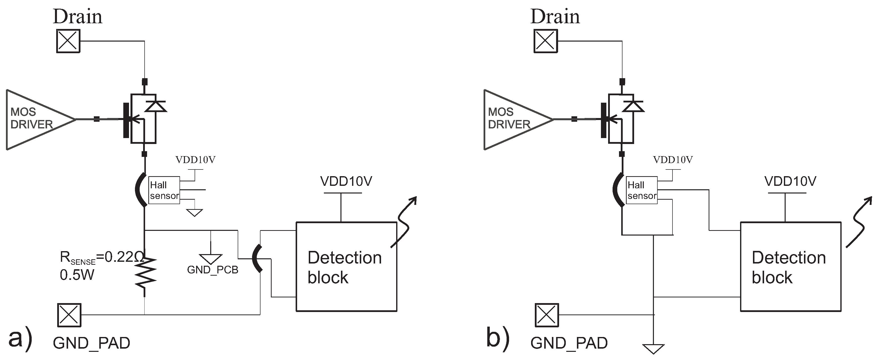
Hall-Effect versus Resistive Setup
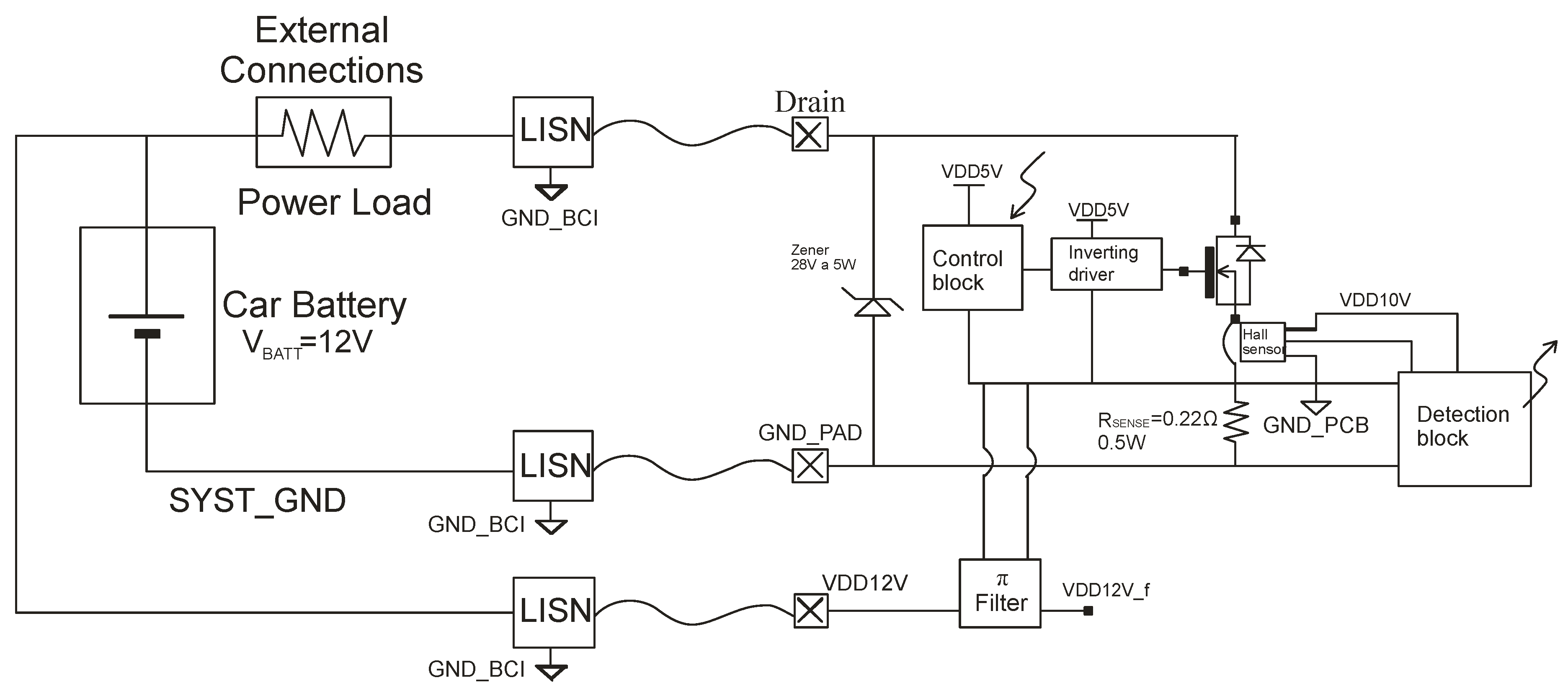
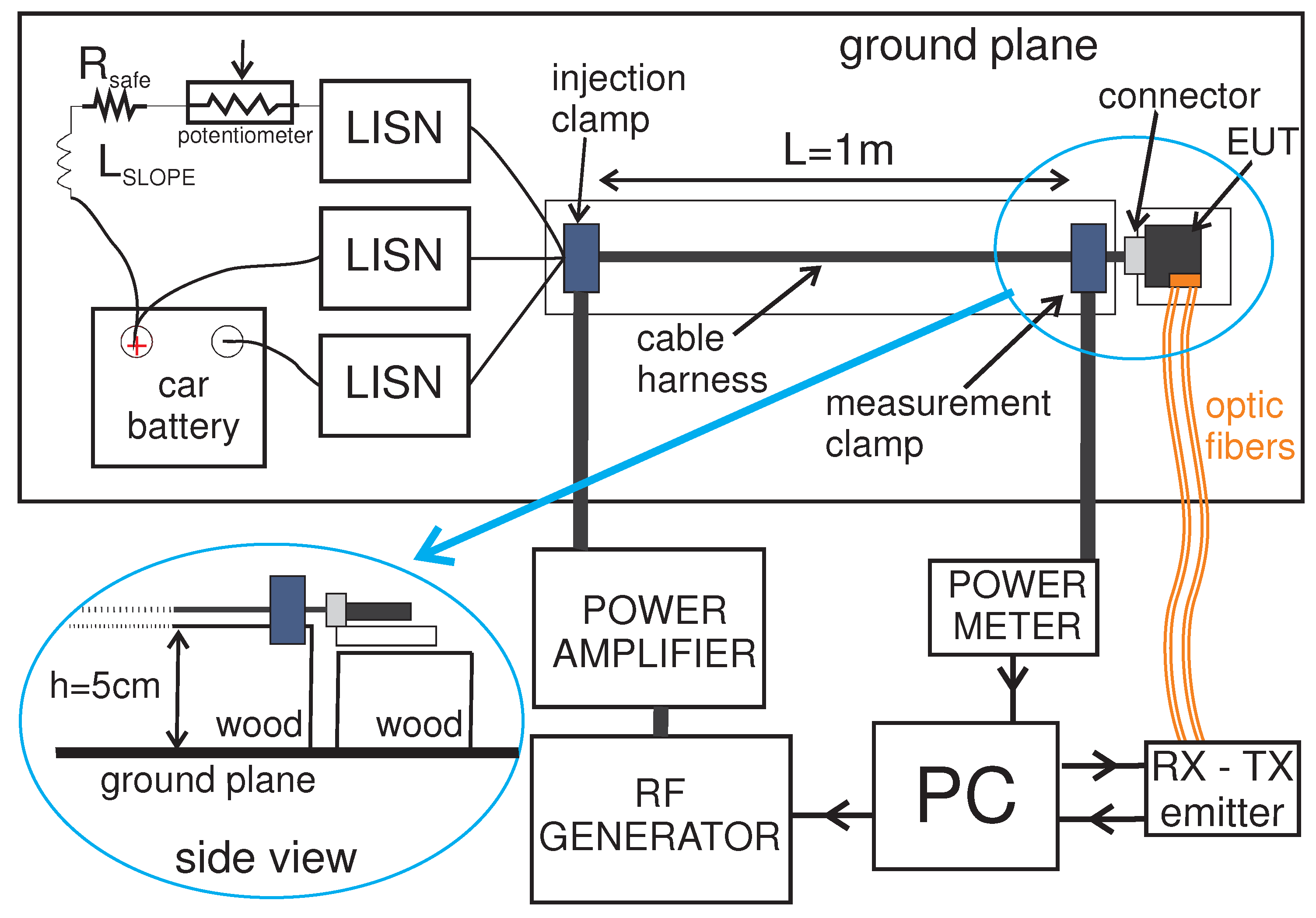
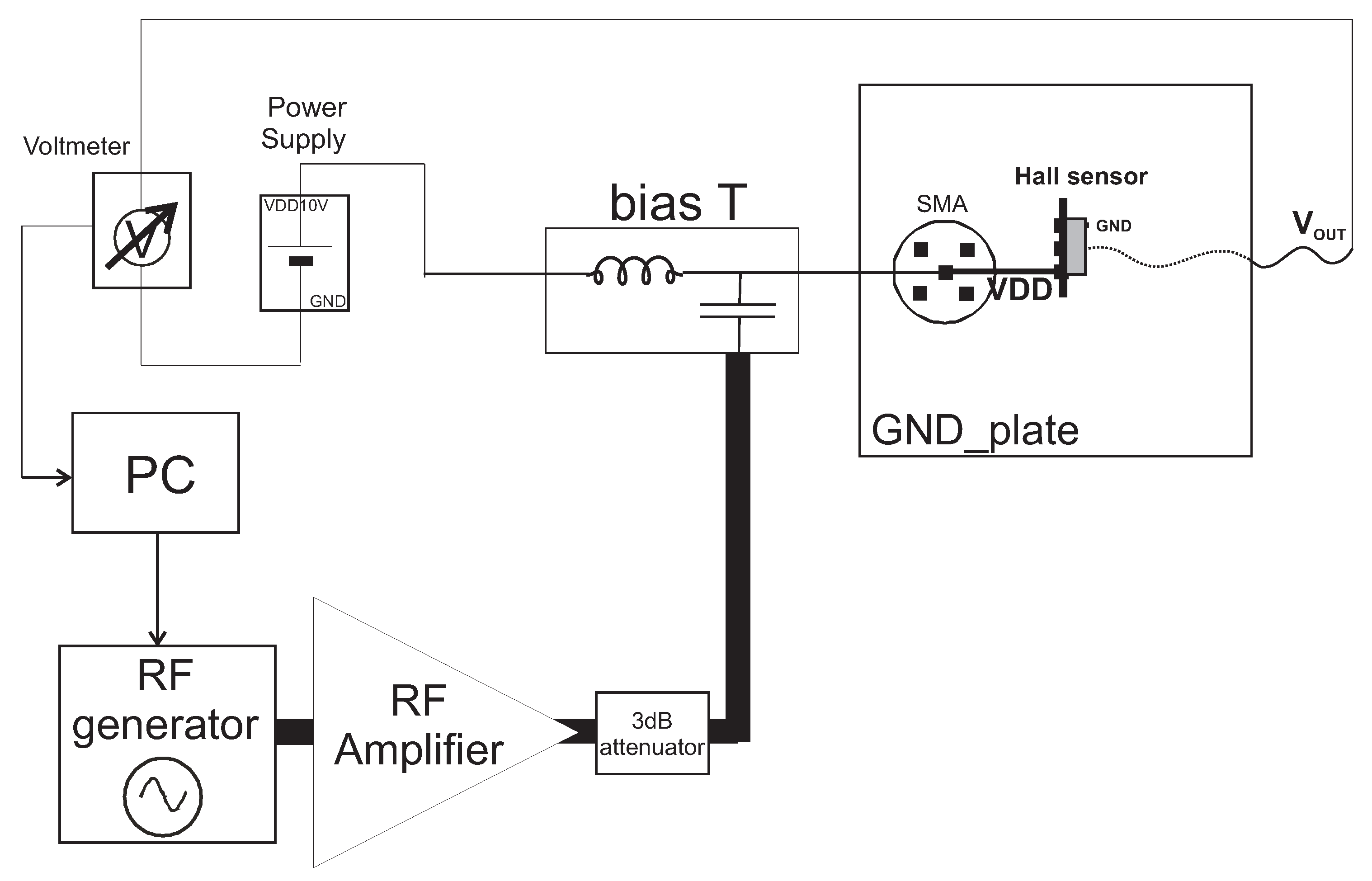
3. Bulk Current Injection (BCI) Test
3.1. BCI Susceptibility Tests
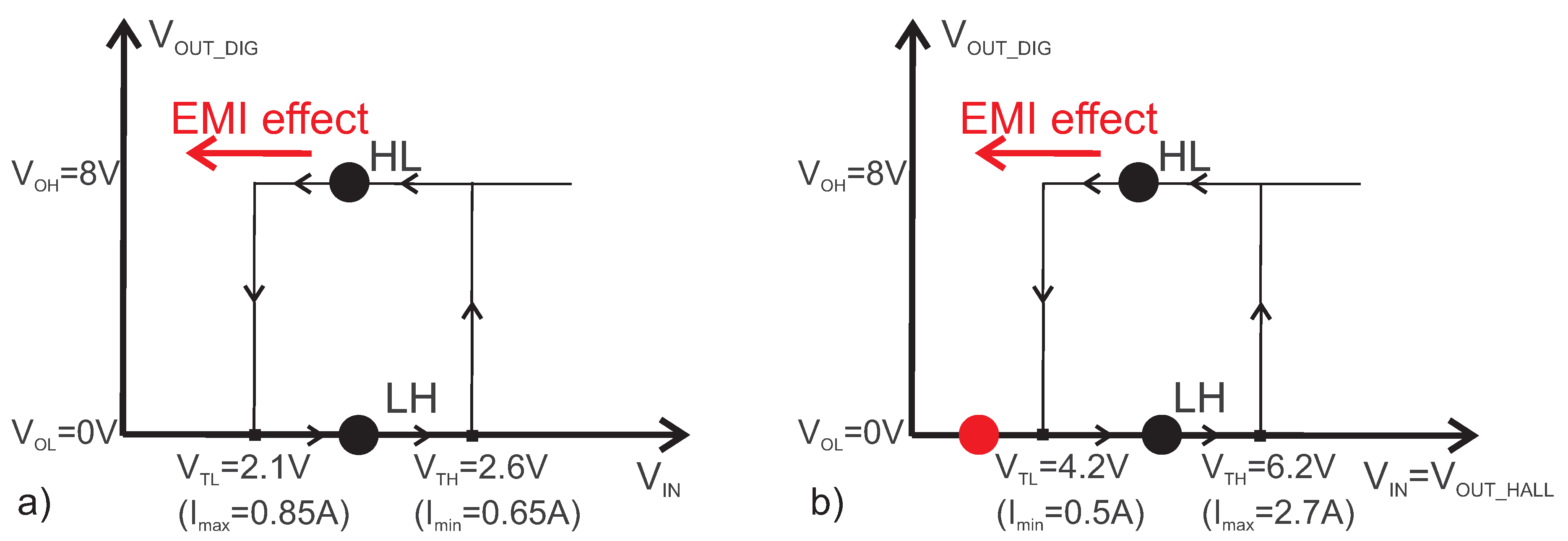
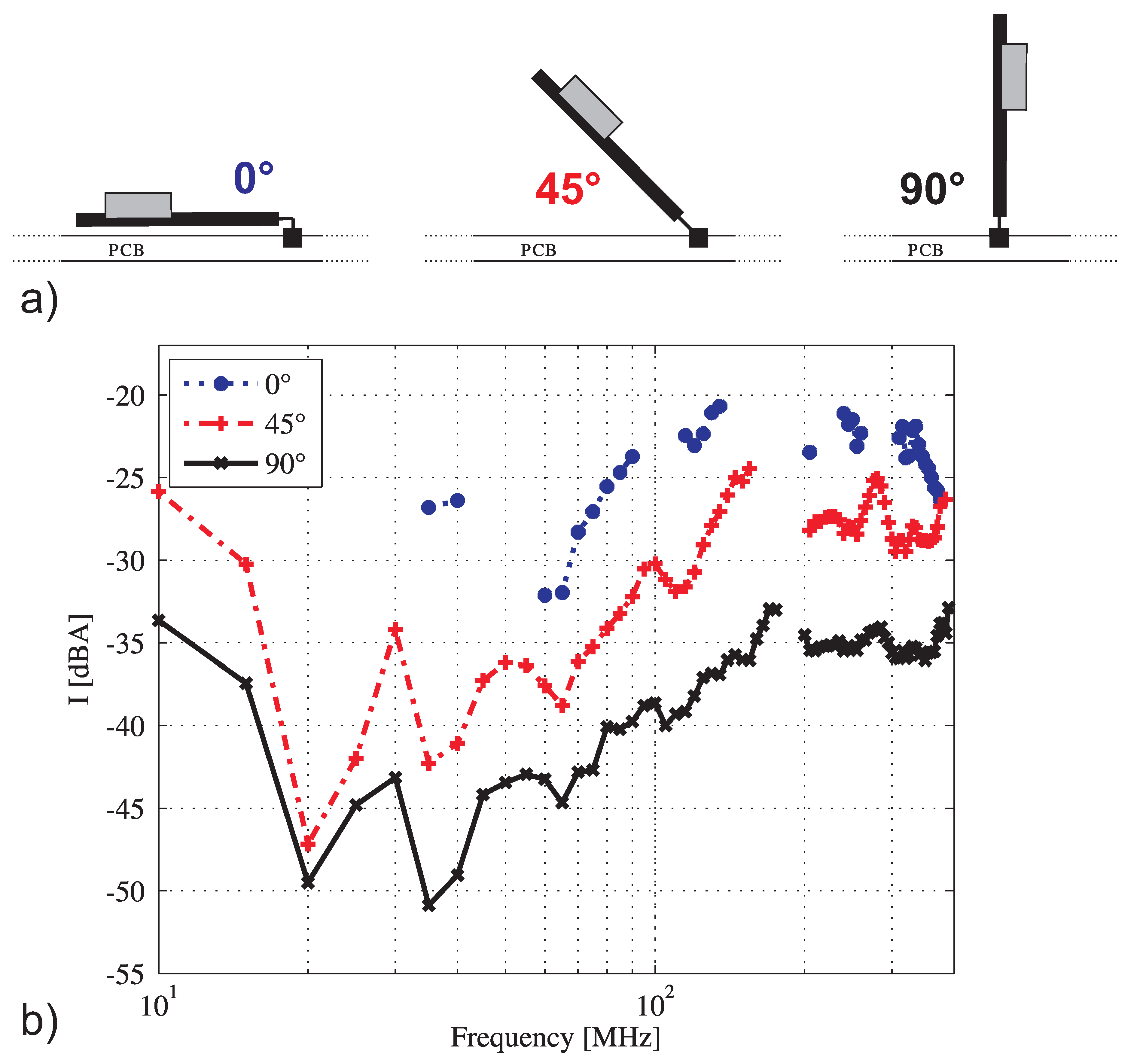
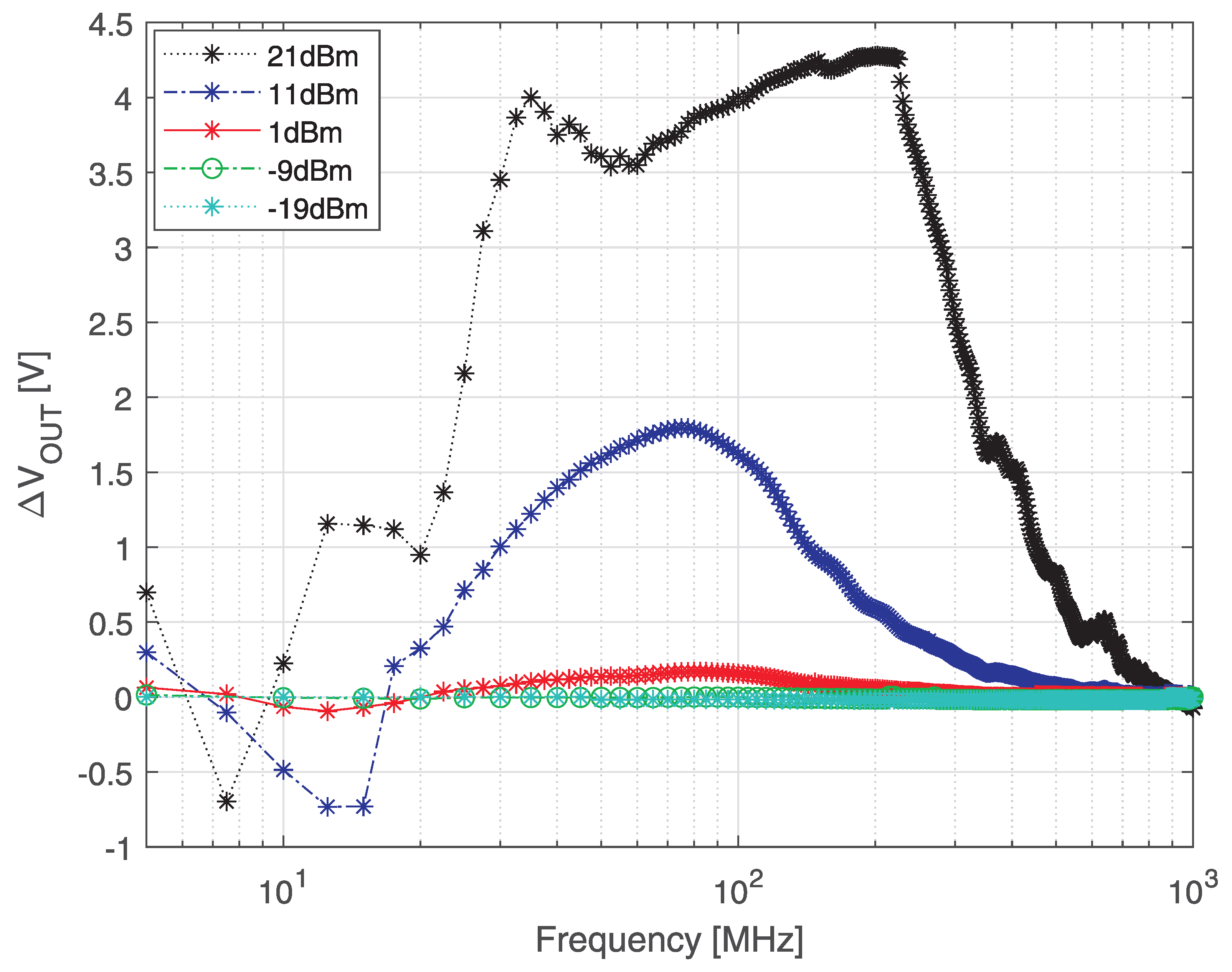
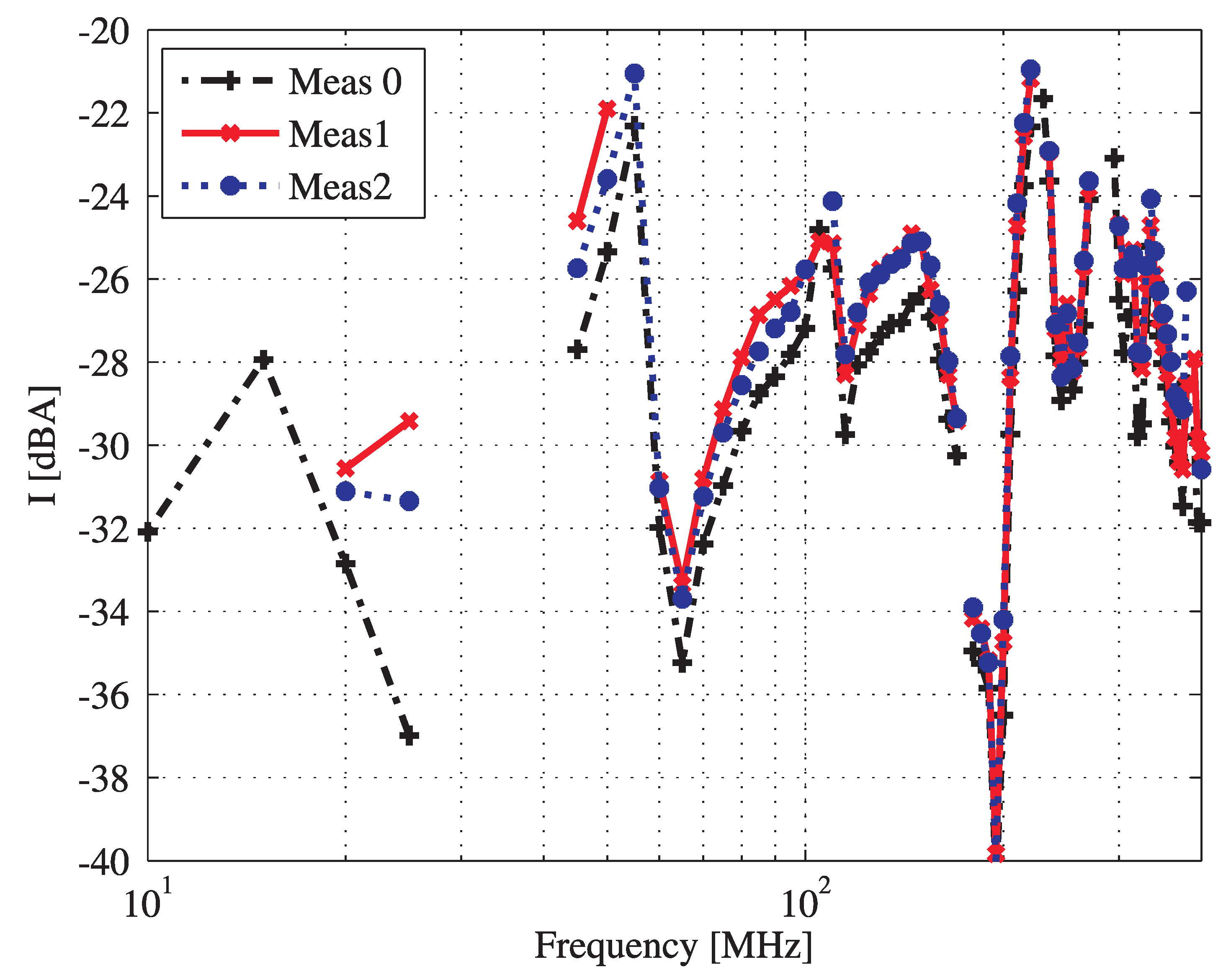
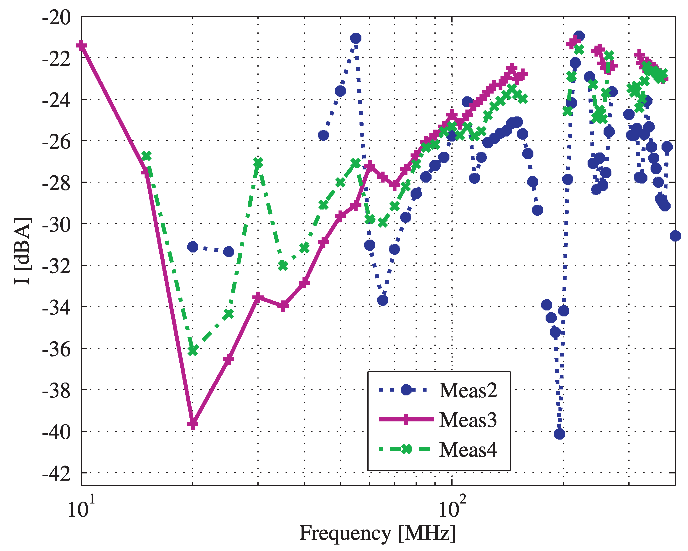
3.2. BCI Test Results
3.3. Discussion
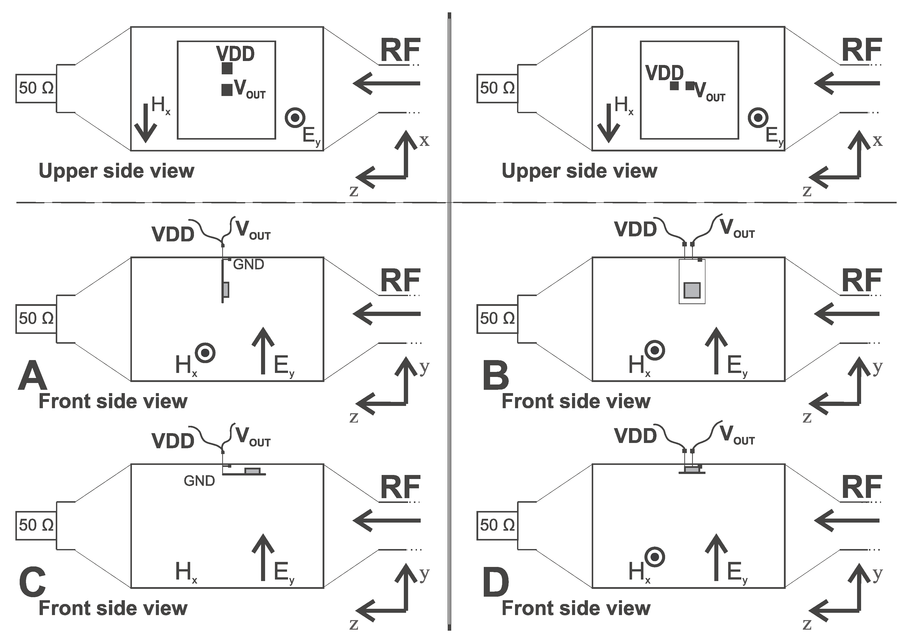
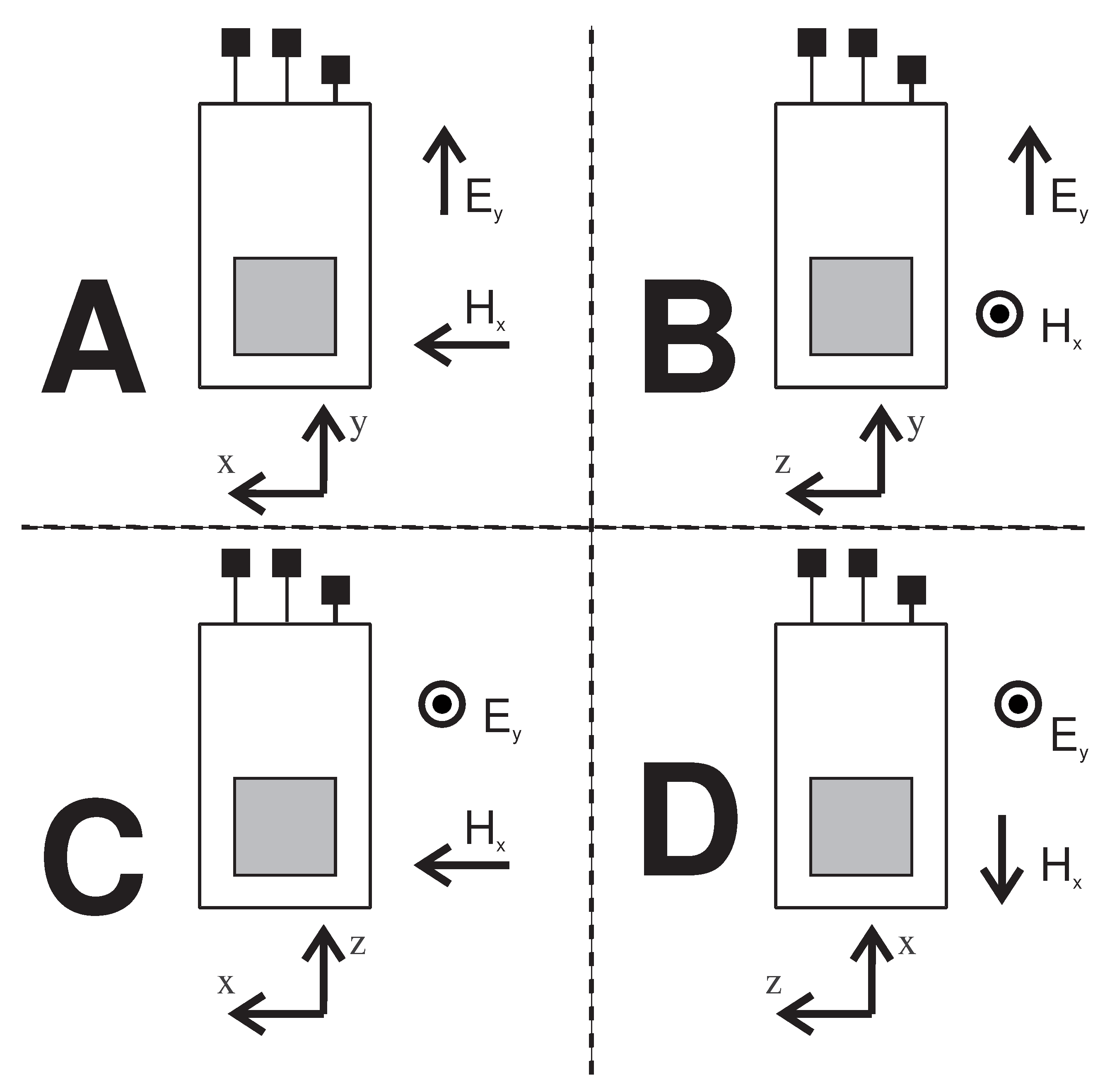
4. Transverse-Electromagnetic (TEM) Cell Tests
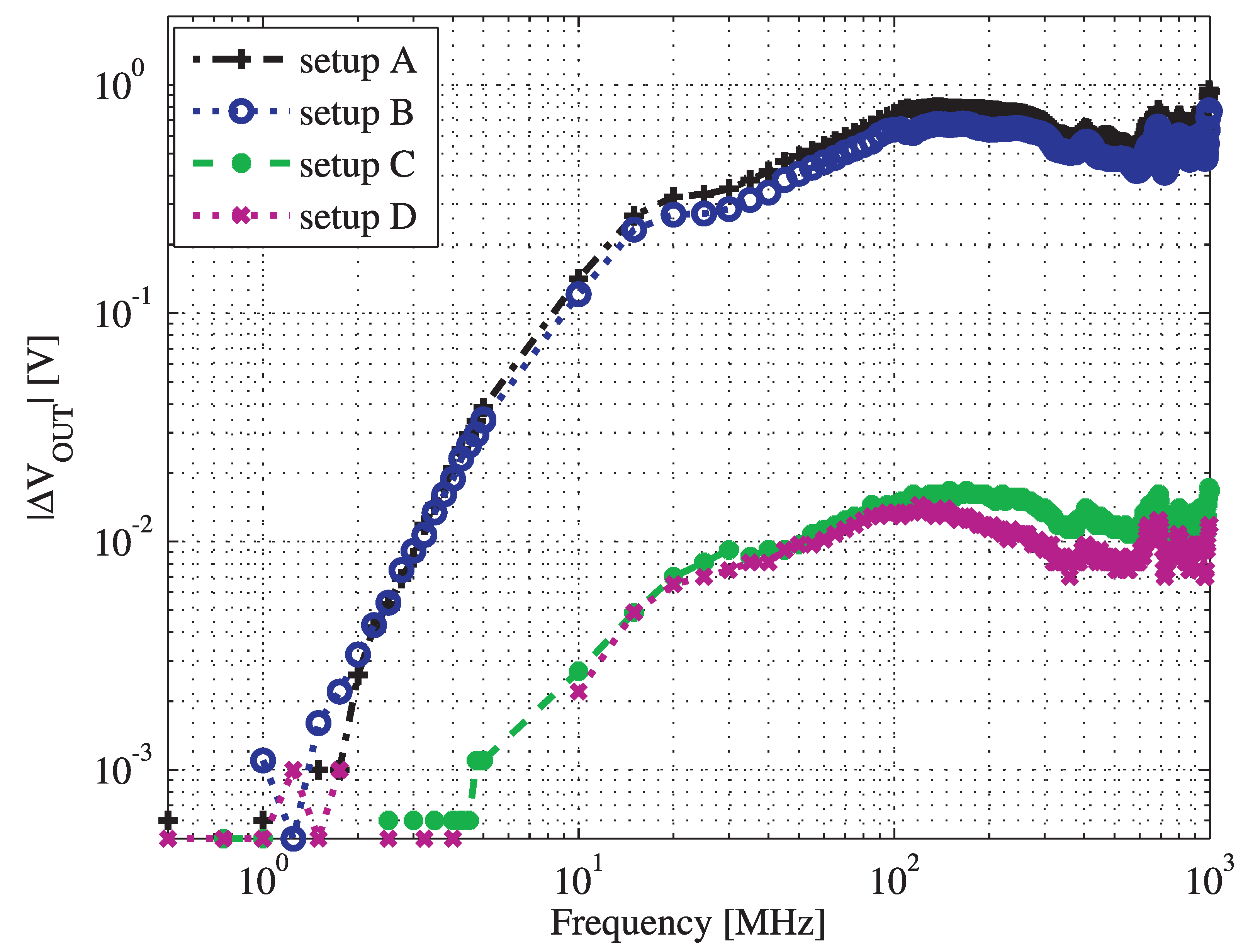
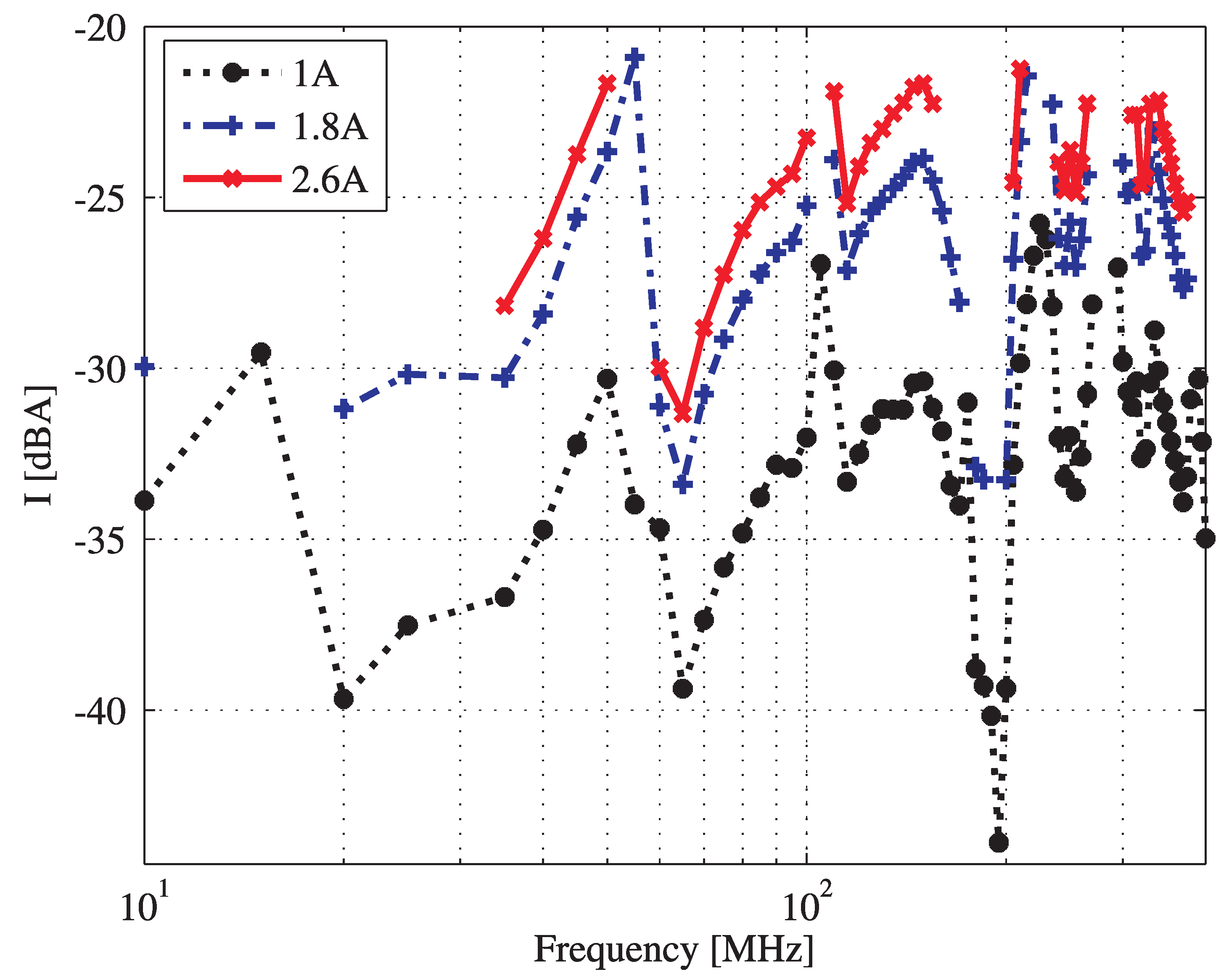
4.1. (TEM) Cell Measurement Result
4.2. Discussion
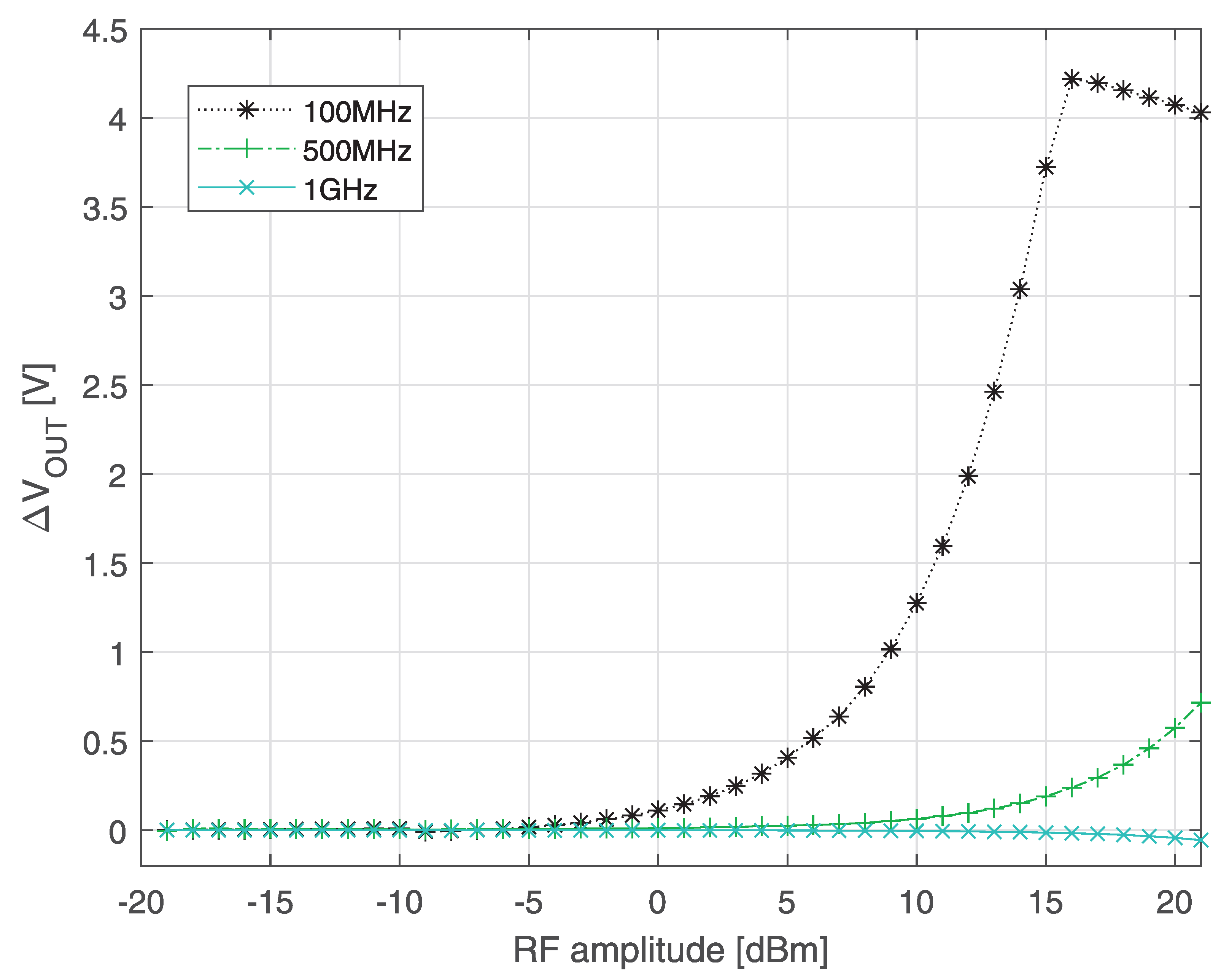
5. Direct Power Injection (DPI)
6. Conclusions
Funding
Conflicts of Interest
References
- Tong, Q.; Chen, C.; Zhang, Q.; Zou, X. A Sensorless Predictive Current Controlled Boost Converter by Using an EKF with Load Variation Effect Elimination Function. Sensors 2015, 15, 9986–10003. [Google Scholar] [CrossRef] [PubMed] [Green Version]
- Min, R.; Chen, C.; Zhang, X.; Zou, X.; Tong, Q.; Zhang, Q. An Optimal Current Observer for Predictive Current Controlled Buck DC-DC Converters. Sensors 2014, 14, 8851–8868. [Google Scholar] [CrossRef] [PubMed] [Green Version]
- Aiello, O.; Fiori, F. A new mirroring circuit for power MOS current sensing highly immune to EMI. Sensor 2013, 13, 1856–1871. [Google Scholar] [CrossRef] [PubMed]
- Aiello, O.; Fiori, F. Current sensing circuit for DC-DC converters based on the miller effect. In Proceedings of the 2013 International Conference on Applied Electronics (AE), Pilsen, Czech Republic, 10–11 September 2013; pp. 1–4. [Google Scholar]
- Huang, K.; Liu, Z.; Zhu, F.; Zheng, Z.; Cheng, Y. Evaluation Scheme for EMI of Train Body Voltage Fluctuation on the BCU Speed Sensor Measurement. IEEE Trans. Instrum. Meas. 2017, 66, 1046–1057. [Google Scholar] [CrossRef]
- Popovic, R.S. Hall Effect Devices, 2nd ed.; Institute of Physics Publishing: Bristol, UK; Philadelphia, PA, USA, 2004. [Google Scholar]
- Aiello, O.; Fiori, F. A New MagFET-Based Integrated Current Sensor Highly Immune to EMI. Elsevier Microelectron. Reliab. 2013, 53, 573–581. [Google Scholar] [CrossRef]
- Aiello, O.; Crovetti, P.; Fiori, F. Investigation on the susceptibility of hall-effect current sensors to EMI. In Proceedings of the 10th International Symposium on Electromagnetic Compatibility, York, UK, 26–30 September 2011; pp. 1–4. [Google Scholar]
- Satav, S.M.; Agarwal, V. Design and Development of a Low-Cost Digital Magnetic Field Meter With Wide Dynamic Range for EMC Precompliance Measurements and Other Applications. IEEE Trans. Instrum. Meas. 2009, 58, 2837–2846. [Google Scholar] [CrossRef]
- Dalessandro, L.; Karrer, N.; Kolar, J.W. High-Performance Planar Isolated Current Sensor for Power Electronics Applications. IEEE Trans. Power Electron. 2007, 22, 1682–1692. [Google Scholar] [CrossRef]
- International Standard ISO 11452-4:2005. Road Vehicles–Component Test Method for Electrical Disturbances from Narrowband Radiated Electromagnetic Energy—Part 4: Bulk Current Injection (BCI). Available online: https://www.iso.org/standard/37414.html (accessed on 6 November 2019).
- International Standard IS0 11452-3:2016. Road Vehicles—Electrical Disturbances by Narrowband Radiated Electromagnetic Energy, Component Test Method Part 3: Transverse Electromagnetic Mode (TEM) Cell. Available online: https://www.iso.org/standard/66829.html (accessed on 6 November 2019).
- IEC 623132-4:2006. Integrated Circuits, Measurement of Electromagnetic Immunity—Part 4: Direct RF Power Injection Method. Available online: https://webstore.iec.ch/publication/6510 (accessed on 6 November 2019).
- Available online: https://www.ansys.com/products/electronics/ansys-maxwell (accessed on 6 November 2019).
- Fischer Custom Communication (FCC). F-130A-1 Injection Current Probe Characterization: Fischer Custom Communication (FCC); FCC: Torrance, CA, USA, 2004. [Google Scholar]
- Fischer Custom Communication (FCC). F-51 Monitor Current Probe Characterization: Fischer Custom Communication (FCC); FCC: Torrance, CA, USA, 2004. [Google Scholar]
- Fiori, F.; Musolino, F. Investigation on the effectiveness of the IC susceptibility TEM cell method. IEEE Trans. EMC 2004, 46, 110–114. [Google Scholar] [CrossRef]
- Fiori, F.; Musolino, F. Measurement of integrated circuit conducted emissions by using a transverse electromagnetic mode (TEM) cell. IEEE Trans. EMC 2001, 43, 622–628. [Google Scholar] [CrossRef]
- Spiegel, R.J.; Joines, W.T.; Blackman, C.F.; Wood, A.W. A method for calculating electric and magnetic fields in TEM cell at ELF. IEEE Trans. Electromagn. Compat. 1987, EMC-29, 265–272. [Google Scholar] [CrossRef]
- Redoute, J.M.; Steyaert, M. EMC of Analog ICS; Springer: Berlin, Germany, 2010. [Google Scholar]
- Richelli, A.; Matiga, G.; Redoute, J.M. Design of a Folded Cascode Opamp with Increased Immunity to Conducted Electromagnetic Interference in 0.18 um. Elsevier Microelectron. Reliab. 2015, 55, 654–661. [Google Scholar] [CrossRef]
- Aiello, O.; Fiori, F. On the Susceptibility of Embedded Thermal Shutdown Circuit to Radio Frequency Interference. IEEE Trans. EMC 2012, 54, 405–412. [Google Scholar] [CrossRef]


© 2019 by the author. Licensee MDPI, Basel, Switzerland. This article is an open access article distributed under the terms and conditions of the Creative Commons Attribution (CC BY) license (http://creativecommons.org/licenses/by/4.0/).
Share and Cite
Aiello, O. Hall-Effect Current Sensors Susceptibility to EMI: Experimental Study. Electronics 2019, 8, 1310. https://doi.org/10.3390/electronics8111310
Aiello O. Hall-Effect Current Sensors Susceptibility to EMI: Experimental Study. Electronics. 2019; 8(11):1310. https://doi.org/10.3390/electronics8111310
Chicago/Turabian StyleAiello, Orazio. 2019. "Hall-Effect Current Sensors Susceptibility to EMI: Experimental Study" Electronics 8, no. 11: 1310. https://doi.org/10.3390/electronics8111310
APA StyleAiello, O. (2019). Hall-Effect Current Sensors Susceptibility to EMI: Experimental Study. Electronics, 8(11), 1310. https://doi.org/10.3390/electronics8111310