1. Introduction
Vertical-cavity surface-emitting lasers (VCSELs) are widely used in high-bandwidth optical interconnects [
1,
2] and 3D sensing applications [
3,
4]. Optical interconnects are part of the Internet structure for quite some time, meeting the demands of the growing bandwidth requirements. The relatively newer 3D sensing applications either rely on time-of-flight (ToF) or structured light beam for depth measurement. VCSEL-based 3D sensing is getting increasingly common for facial recognition in smartphones and object tracking in automobiles and robots using LiDAR (Light Detection and Ranging). Modern optical interconnects and 3D sensing applications require short-pulsed, high-power driving circuits for VCSELs.
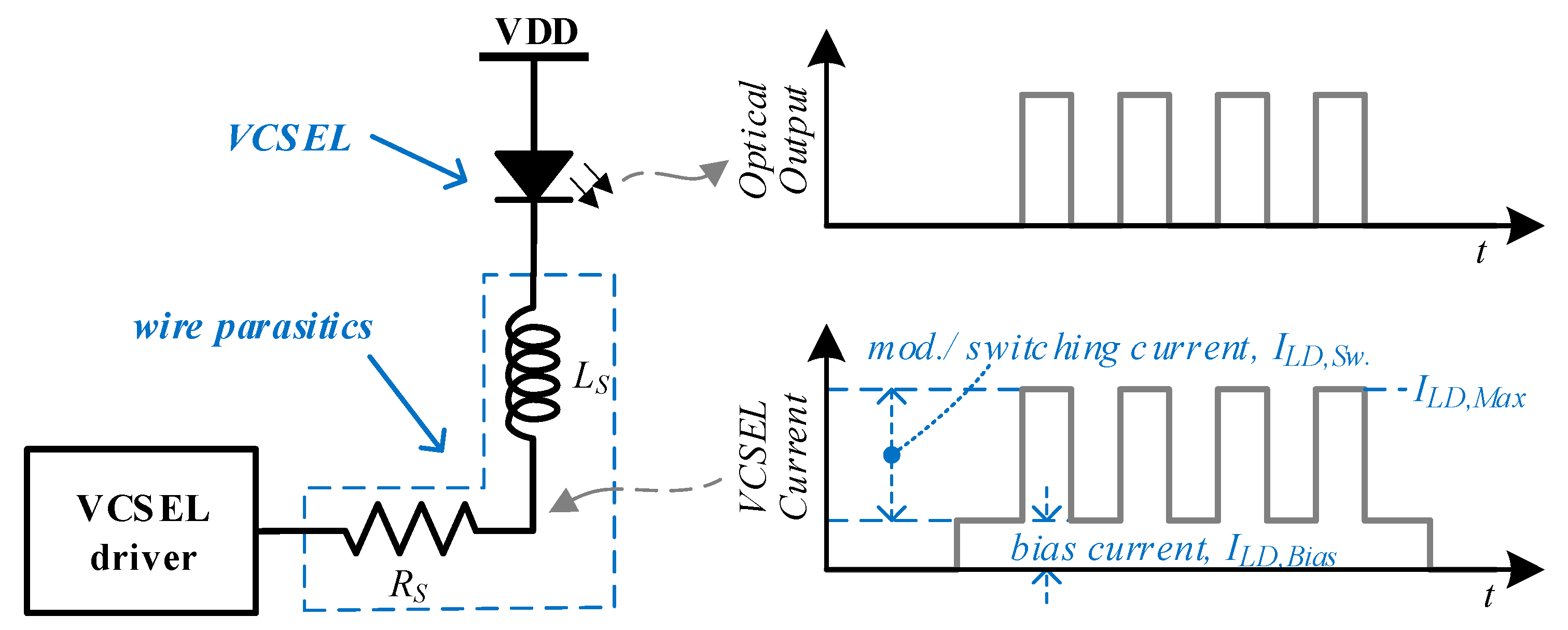
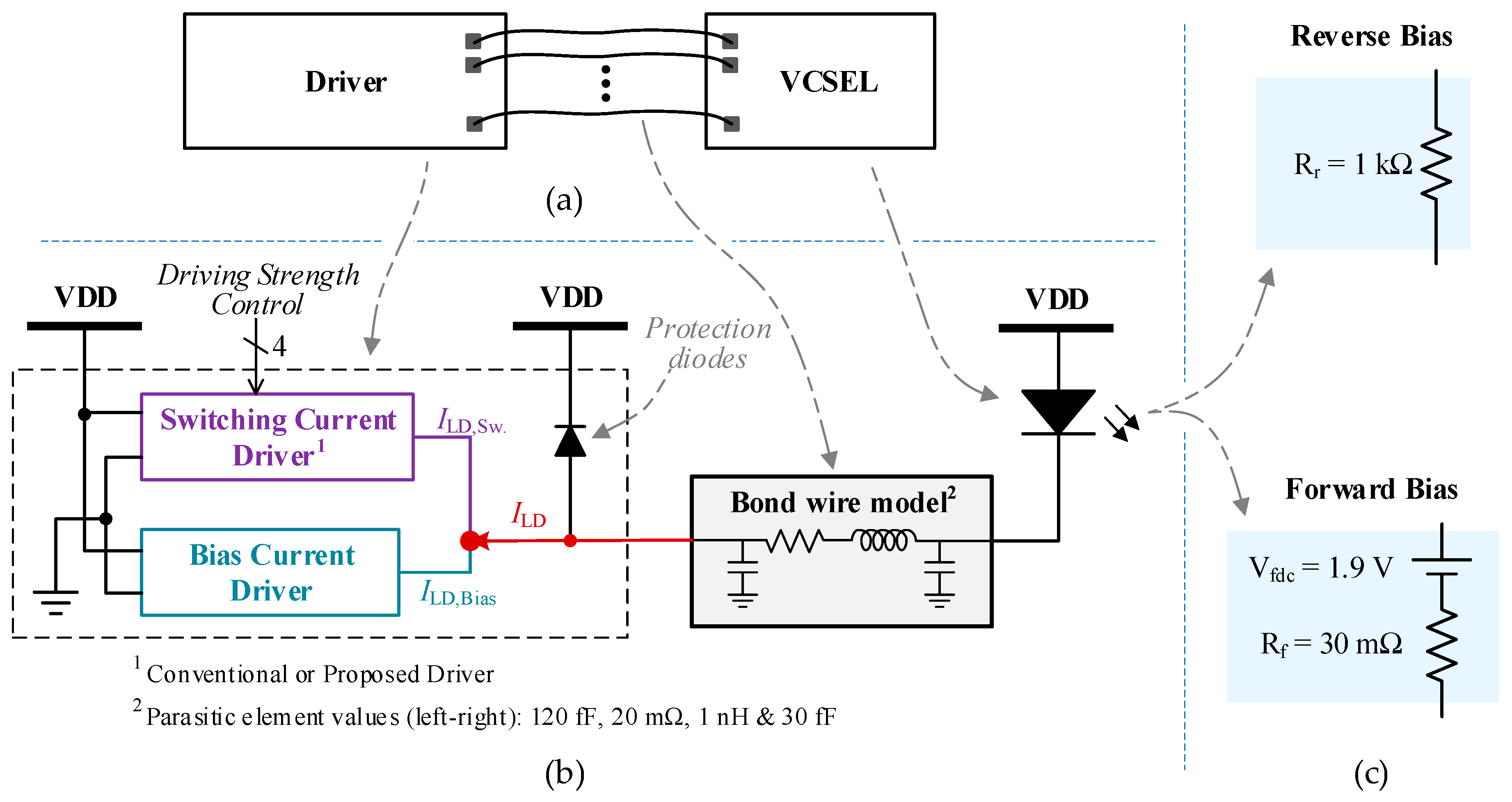
Figure 1 illustrates an example circuit connecting a VCSEL and its driver, emphasizing the parasitic resistance and inductance of the wire. With the required pulse widths (of the VCSELs) approaching one nanosecond or less, it becomes challenging to design its driver circuit [
5]. This is because the parasitic components of the wire, connecting VCSEL with the driver, restrict fast transitions in the current. Some advanced methods to reduce parasitics include bonding the driver die directly to the printed circuit board (PCB) [
6,
7], and bonding the driver and VCSEL dies directly to each other without a PCB [
8,
9].
The methods in [
6,
7,
8,
9], however, result in increased cost, and may not be able to meet the transition requirements on their own. Additional methods are therefore needed to ensure sharper transitions to meet the required specifications.
Due to low-cost and low-power requirements, the Complementary Metal Oxide Semiconductor (CMOS) is a suitable choice for the implementation of the driver circuits [
10]. Also, it is strongly recommended to use an integrated driver circuit which can reduce the wire parasitics and thus allow faster signal transitions [
11]. Many drivers use a large supply voltage to achieve the desired rate of change in the current by overcoming the parasitic inductance of the wire [
12,
13]. A large voltage supply, however, results in excessive power consumption, making the driver unsuitable for mobile applications. Some researchers have used an additional external boosting inductor to create a momentary boost in the supply voltage [
10,
14]. For such drivers, additional circuits and wires are required to charge the large boosting inductor, resulting in increased power consumption and area overhead. Therefore, the additional external components make the inductor boosting method less suitable for fully integrated applications.
On the other hand, switched capacitor circuits offer the benefit of on-chip integration, which makes them suitable for mobile applications [
15,
16]. Moreover, with deep submicron processes offering high density on-chip capacitance, high power applications can be addressed. A capacitor boosting technique is presented in [
17], which uses a flying capacitor to boost (double) the VDD to have a sharp rising of the VCSEL current. This technique, however, requires many additional wires, and does not support adjustable current levels. In addition, it has extra metal–oxide–semiconductor field-effect transistors (MOSFETs) in the driving current path, posing limitations for high-speed and high-power applications. Additional research is needed to overcome the limitation of the previous drivers for high-power applications, minimize the power overhead and eliminate the needs for external components.
This letter proposes a fully integrated, switched capacitor based, negative supply boosting during the rising transition to overcome the parasitics. The proposed VCSEL driver also supports multiple current levels, with significantly lower power consumption compared to previous boosting methods mentioned above. The proposed driver, being fully integrated and power efficient, targets 3D sensing for mobile platforms as the main application. It is, however, possible to use the driver in a vast number of applications from optical interconnects to biomedical devices.
Section 2 analyzes the rise time of the VCSEL current in presence of the parasitic elements.
Section 3 presents the proposed architecture and its analytical model.
Section 4 discusses circuit implementation and evaluates the performance of the proposed architecture. Finally, a discussion on the interpretation and usefulness of the simulation results is presented in
Section 5, followed by conclusions in
Section 6.
2. Analysis of the VCSEL Rise Time
To explore low power methods to reduce the rise time of the VCSEL current, consider a typical VCSEL connection with the driver circuit shown in
Figure 1. There are two types of current flowing through the VCSEL or Laser Diode (LD), which are bias
and modulation/switching current
[
1]. During operation, the bias current stays constant while the switching current has a pulsating behavior with high switching frequency. The parasitic inductance of the wire resists sudden changes in the switching current and degrades the rise and fall time, thereby limiting the switching frequency. Due to the presence of these parasitics, it can be challenging to achieve a sub-nanosecond rise time at large switching current levels [
5]. The purpose of the bias current is used to overcome the threshold current of the VCSEL, while producing no optical output. Without the bias current, the switching current would have longer transition times, with the total current going from 0 to
.
The current flowing through the inductor (and the VCSEL) of
Figure 1, during the rising transition, can be calculated by (1).
Here,
VRL is the voltage drop across the wire (inductor and resistor),
is inductance,
is resistance and
is the time instant. The voltage drop on the wire is expressed by (2).
In (2),
is the supply voltage,
is the forward voltage drop of the VCSEL and
is the voltage drop across the MOSFETs of the driver. To find the rise time (10% to 90%) for a target current
, we can start by re-arranging (1), to get the rise time by (5).
It is evident from (5) that the rise time of the current can be reduced by reducing the parasitic inductance. Generally, the width of the trace (connecting the driver to the VCESL) is kept minimum, in order to have low parasitic values. To explore additional methods of reducing rise time, we need to investigate the dependency of
on
.
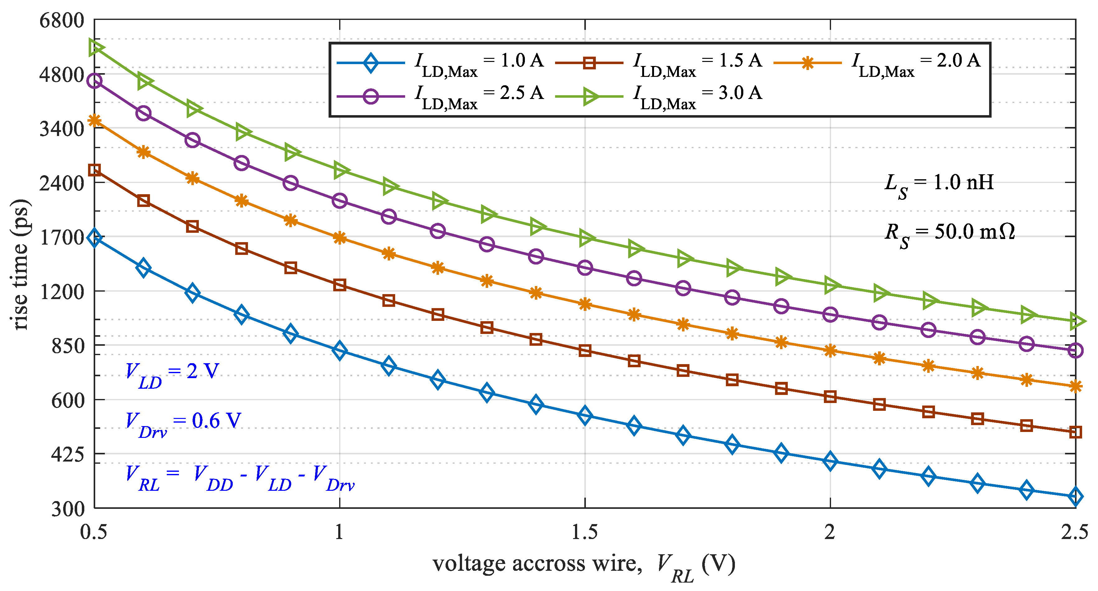
Figure 2 illustrates the change in rise time over a range of
using (5), for
in the range of 1A to
.
Figure 2 assumes a typical parasitic model for the bonding wires and PCB traces,
,
. It can be observed from
Figure 2 that the rise time can be decreased by increasing the voltage across the wire. As expressed in (2), the voltage across the wire can be increased by (1) decreasing
, (2) decreasing
, and (3) by increasing the power supply voltage. Using a larger power supply [
12,
13] or using a temporary boosted supply [
10,
14,
17] are known to decrease rise time. Another notable observation is that the voltage required across the wire varies with
, for the same rise time. Therefore, to avoid overshoot while maintaining the rise time, the voltage drop across the wire must be decreased with the decrease in
.
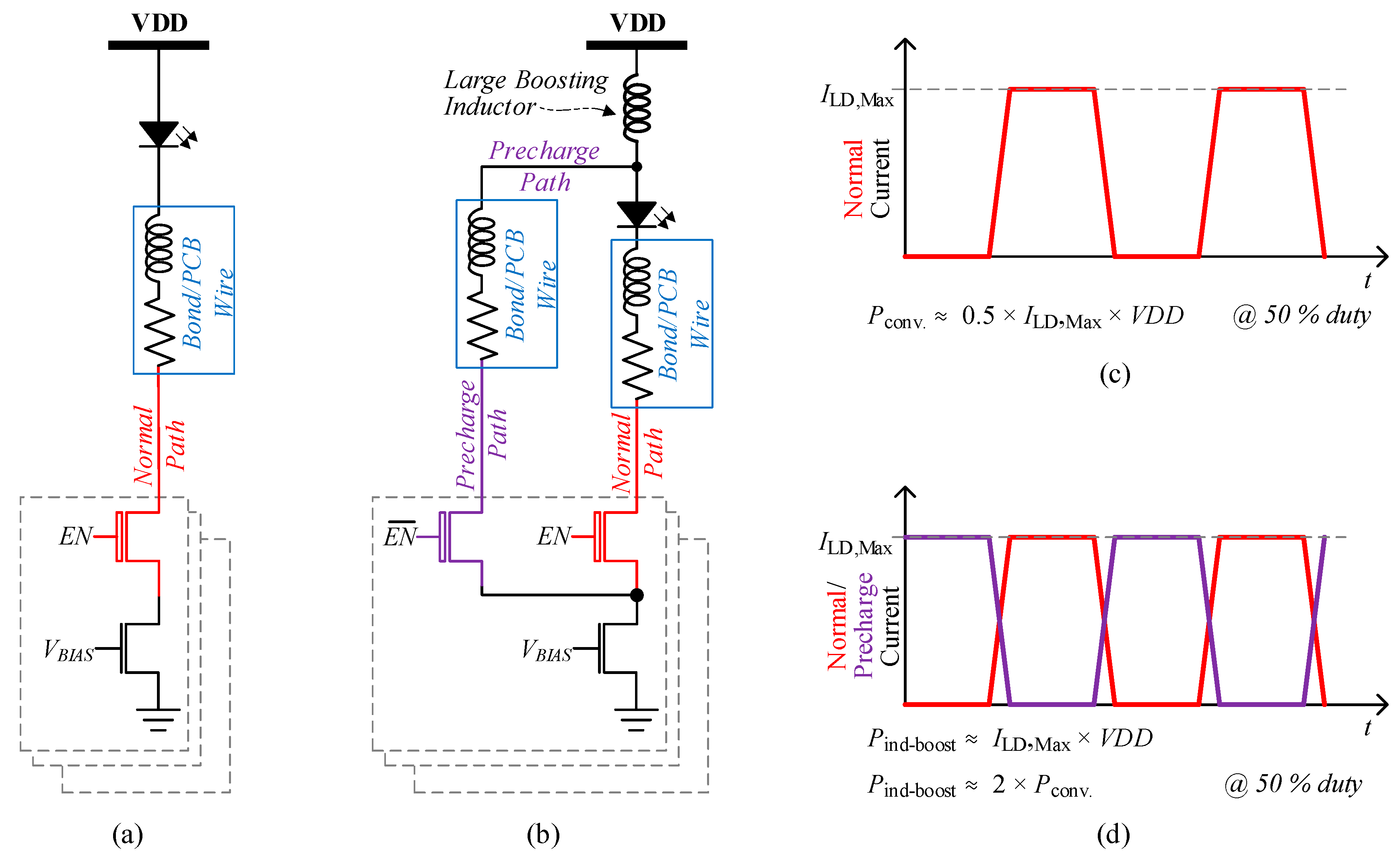
A conventional driver circuit is shown in
Figure 3a with its current waveform in
Figure 3d. The external inductor-based voltage boosting method employed in [
10,
14], which boosts the voltage during the rise time, is shown as a simplified circuit in
Figure 3b. During the off-period (
EN = 0), the boosting inductor is charged to
, as shown in
Figure 3d. During the on-period (
EN = 1), the normal path connects, and the boosting inductor momentarily raises voltage on the anode of the VCSEL to force current
. This, however, requires complex driver circuitry, which incurs excessive area overhead in addition to external inductor and wires. Furthermore, the power consumption doubles, since its pre-charge current continuously flows even during the off-period, as demonstrated by comparing
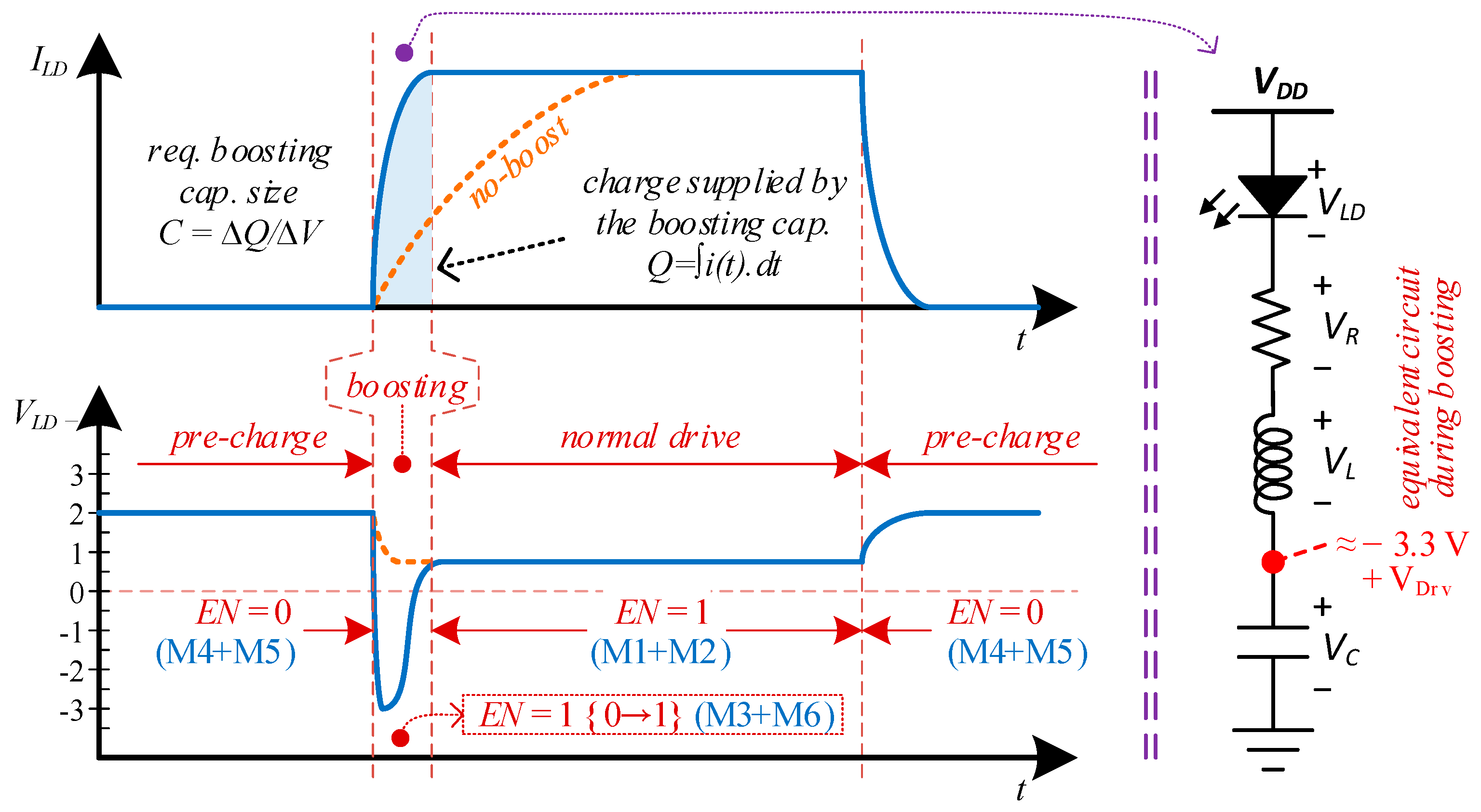
Figure 3c,d. In contrast, the technique proposed in this paper boosts the supply voltage up to 2x VDD, during rising transition, by creating negative VDD. The proposed technique accomplished a short rise time without any external components or wires.
3. Negative Voltage Boosting
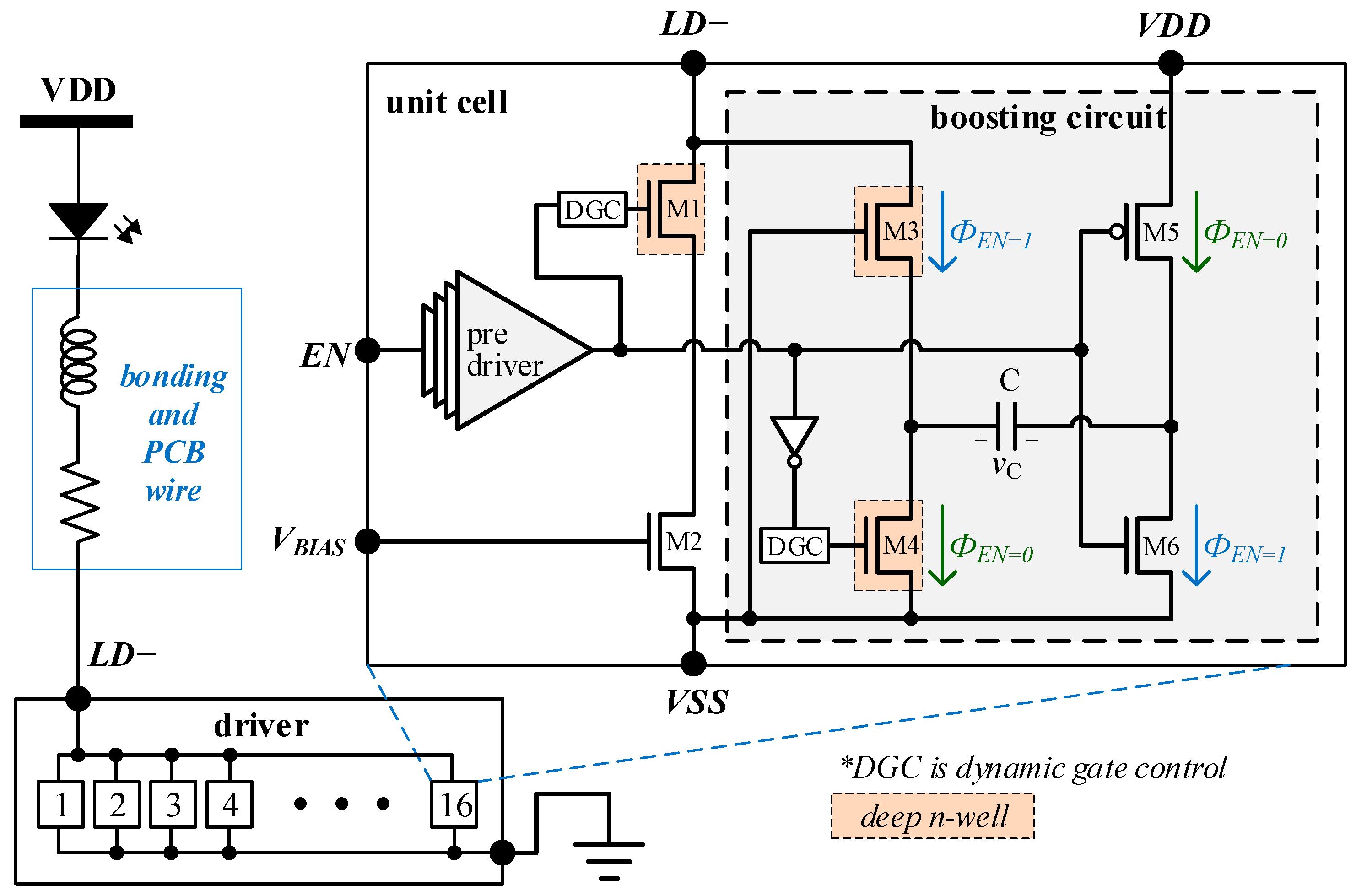
To achieve faster rising transition and low power consumption, a precalculated magnitude and duration of the supply voltage boosting is needed. The proposed design is shown in
Figure 4, which contains an array of sixteen driving cells with individual boosting circuits. The individual boosting circuits allow the proposed driver to provide multiple switching current levels by producing only the required amount of boosting charge to avoid overshoot. Due to the use of an integrated boosting circuit, the proposed driver does not require external components like the large inductor of [
10,
14].
The boosting circuit provides up to 2xVDD boosting by generating a short-lived negative VDD using the MOSFETs and the capacitor in the boosting circuit. The circuit operation of the proposed driver can be divided in to three phases as shown in
Figure 5, which are pre-charge, boosting and normal driving phases. During the pre-charge phase, the built-in capacitor is charged to VDD in opposite polarity, while no current is supplied to the VCSEL. During the boosting phase, the capacitor is connected to provide negative VDD (−VDD), which can drive the VCSEL rapidly to the target level. During the normal driving phase, the boosting capacitor is disconnected, and thus M1 and M2 flow a fixed amount of current through the VCSEL.
During boosting, the amount of charge supplied (by the boosting capacitor) depends upon the final level of the VCSEL current and the rise time; i.e.,
, as shown in
Figure 5. Since a short rise time is provided by the proposed driver, the charge supplied by the capacitor during the short rise time is also small. Due to the relation of
, a small-sized boosting capacitor is needed in the proposed driver, resulting in small overhead in the area and power consumption. To supply an appropriate amount of charge for sixteen VCSEL current levels, the proposed driver reduces the effective boosting capacitor size when the target current level is low. This is accomplished by distributing small boosting capacitors inside each unit cell instead of one large shared capacitor.
In
Figure 4, when EN = 0, the boosting capacitor in each unit cell is pre-charged to −3.3 V, using M4 and M5. When EN switches to 1, M6 connects the negative terminal of the capacitor to ground. The potential on the source of M3 goes to −3.3 V, causing M3 to turn on and bring LD− to approximately −3.3 V. The capacitor charge depletes as the VCSEL current rises, causing M3 to turn off when
is approximately −550 mV (
, the threshold voltage
of MOSFET in the employed process technology is 550 mV).
As some of the MOSFETs in the circuit are exposed to negative voltages, there are two issues to be addressed. First, both M4 and M1 are exposed to negative voltage on their drain terminals when they should be off, which causes them to continue to conduct. To overcome this problem, the dynamic gate control presented in [
18] is incorporated. Dynamic gate control pulls the gate terminal to negative voltage to keep the MOSFET in the cut-off mode, although the original gate voltage would have been zero. Second, the negative drain voltage causes the bulk-drain pn-junction of MOSFETs to become forward biased. To overcome this problem, a body-switching technique presented in [
18] is exploited. The body switching circuit connects the bulk terminal to the lower potential node between drain or source. As the bulk voltage of the MOSFET may change from the ground potential, we choose a CMOS process technology with deep n-well to create an isolated p-well to act as substrate for M1, M3 and M4.
3.1. Estimating the Size of the Boosting Capacitor
To estimate the required boosting capacitor size, we can apply the Kirchhoff voltage law (KVL) (during boosting, when M3 and M6 are operational), which gives (6). By solving the 2nd order differential equation of (6) for voltage across the capacitor, we can obtain (7).
In (7),
and
, which are the real and imaginary part of the roots of the characteristic equation.
and
are defined by the initial conditions. When the boosting phase starts,
is the initial voltage on the capacitor and
is the initial current through the inductor/capacitor (same as the bias current of VCSEL). To ensure maximum utilization of the added boosting circuit, the response of (6) must be under-damped, which can be verified by
. Similarly, the current through the capacitor (and the VCSEL) can be expressed by
, which is expanded to (8):
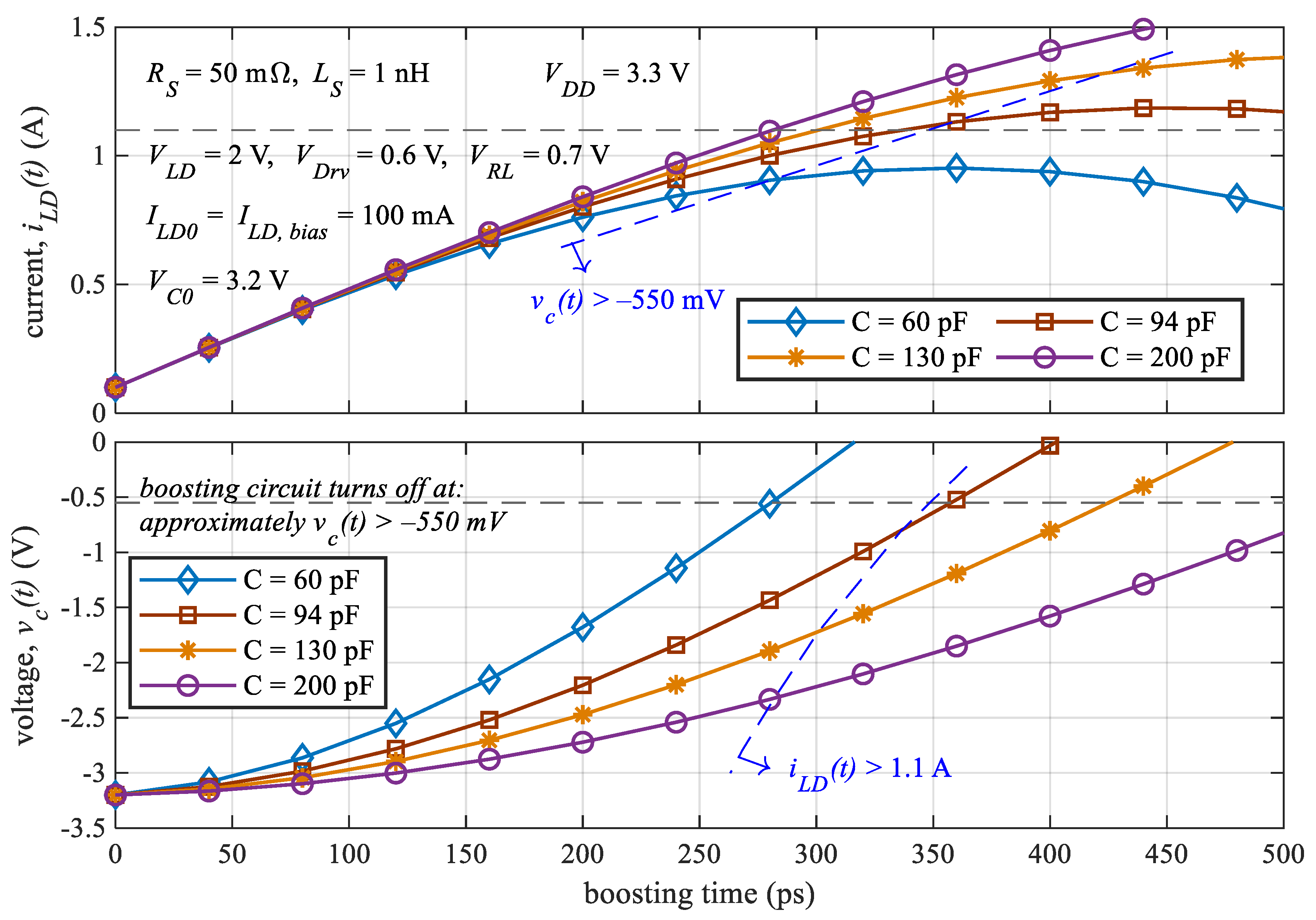
Now, we can plot (7) and (8) to estimate the total required capacitance. For example,
Figure 6 shows the current and voltage plot using (7) and (8), for various sizes of the boosting capacitor, targeting the switching current of 1 A with a bias current of 100 mA. Considering charge-sharing losses in the circuit, initial capacitor voltage
of −3.2 V (instead of −3.3 V) is used, which predicts the maximum capacitor size to be 94 pF. For the maximum capacitor size, the current and voltage curves reach 1.1 A and −550 mV, respectively, at nearly the same time. It is important to choose an optimal maximum capacitor size, since the boosting circuit automatically disconnects itself only when
. If we select too large a capacitor, the current may exceed the target level before the capacitor disconnects at
, causing overshoot. It is possible, however, to use a smaller boosting capacitor for relaxed rise time requirements. For smaller boosting capacitor sizes, the boosting circuit does not bring the current to the required level, since the capacitor voltage reaches −550 mV too early, which will cause the rise time to be prolonged.
3.2. Design Procedure
In order to exploit the benefits of the proposed architecture for a given set of constraints ( and ), the following procedure can be adapted.
Choose nominal VDD level.
Calculate the voltage drop across the wire parasitics (, using (2).
Plot (7) and (8), for various capacitor sizes.
Choose the size of the boosting capacitor from the plot of (7) and (8),
In step 4, the duration to reach from to represents minimum achievable rise time, using the current VDD level.
If the required rise time ,
If the required rise time ,
Implement the circuit in
Figure 4 with the chosen boosting capacitor size
4. Results
For comparison, both conventional driver (without boosting circuit) and the proposed driver (with boosting circuit) are designed in 130-nm 3.3 V CMOS process using Cadence Virtuoso and simulated using Cadence Spectre. Both the drivers include 16 switching current cells, allowing configurable switching current strengths up to 1 A with a resolution of 62.5 mA. The maximum boosting capacitor of 94 pF (pre-determined using the analytical model of (6) and (7)) is divided equally among all the unit cells. The simulation setup realizes a die-to-die bonding scenario of
Figure 7a, as shown in
Figure 7b. A piece-wise linear Verilog-A VCSEL model is used for the simulations, targeting VCSELs such as shown in [
19].
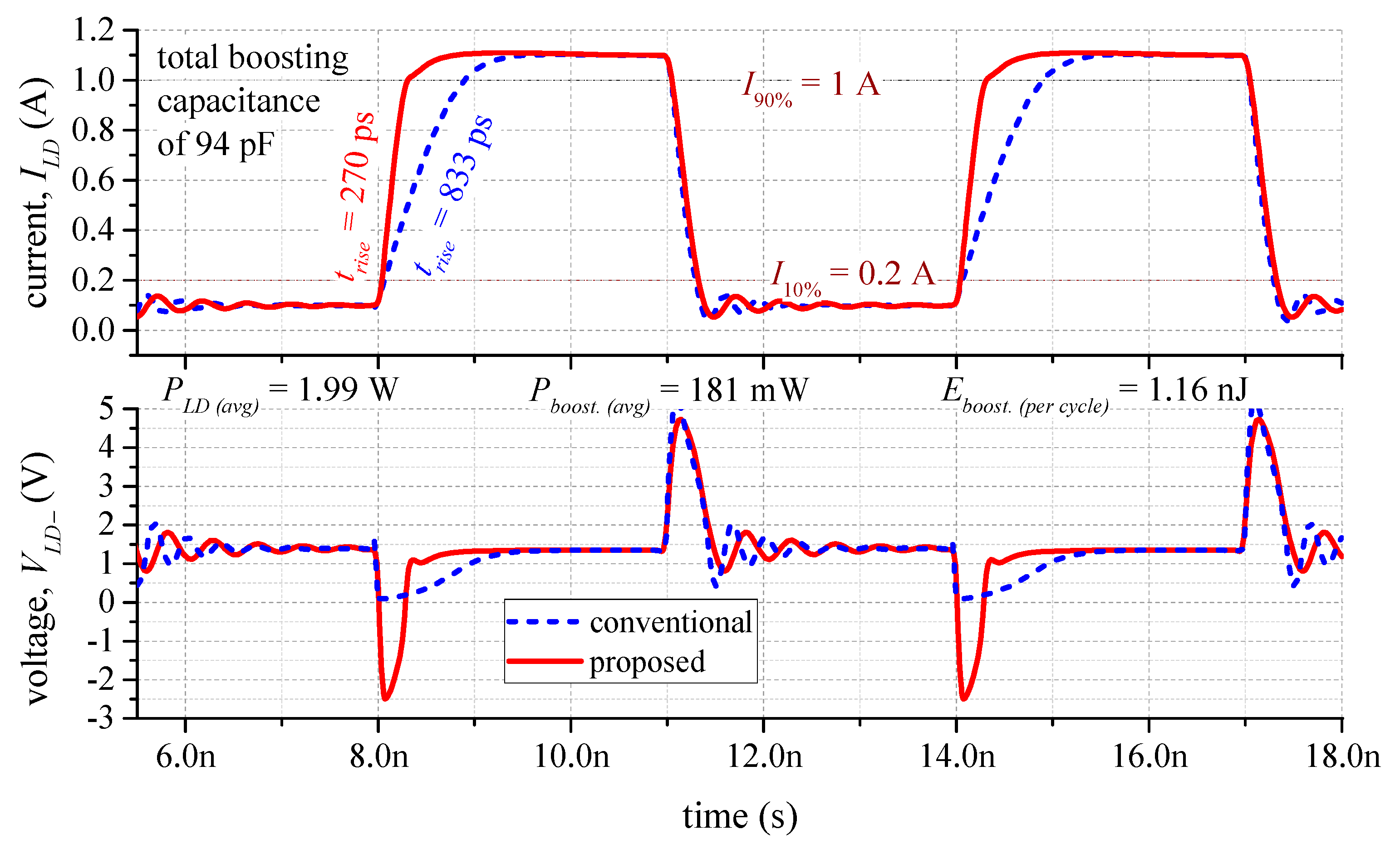
Figure 8 shows the simulation results obtained by operating all 16 unit cells, providing the maximum switching current of 1 A and the bias current of 100 mA. The conventional driver (blue curve) offers a current rise time of 833 ps, while the proposed driver (red curve) offers 270 ps—a notable reduction of 67.6%. The rise time reduction is achieved at the expense of a 57% increase in the unit cell area. The voltage waveform of the proposed driver (red curve) shows that the LD− node of
Figure 4 is pulled to negative voltage, causing a large voltage-drop across the parasitic elements of the wire, which results in a sharper rise in current. During the falling transition, the voltage
reaches as high as 5 V in both the conventional and the proposed driver. This is because the parasitic inductance of the wire resists the change in current from
to
by raising the voltage on the
terminal. Reverse-biased diodes are added between
and VDD to sink the current during the falling transition.
For the above simulations, the VCSEL consumes an average power of 1987 mW, while the boosting circuit consumes 181 mW (only 10% overhead), for the target current pulses with a width of 3 ns and a period of 6 ns—a typical specification of 3D sensing/ranging applications [
20]. On the other hand, to achieve a rise time of 270 ps using the conventional driver, a supply of 5.3 V is needed for the VCSEL, consuming an average power of 3200 mW (47.6% higher than the proposed technique). The energy consumed per boosting cycle by the boosting circuit and VCSEL is 1.16 nJ and 11.92 nJ, respectively. When the target specification of the pulse requires larger width or a longer period, the ratio of boosting circuit to VCSEL power consumption can be further reduced.
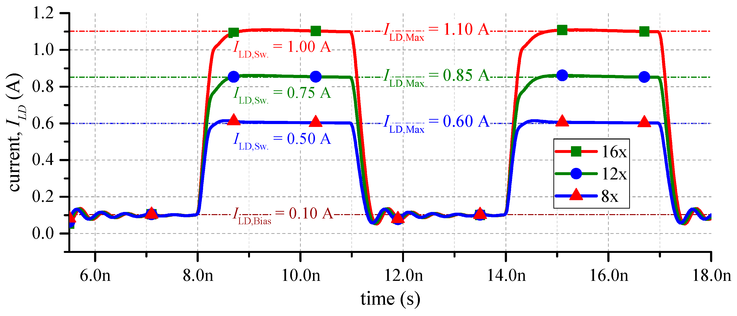
A second set of circuit simulations is carried out to illustrate the operation of the proposed driver for multiple current levels.
Figure 9 shows simulation results when using all 16 cells (16x), 12 cells (12x), and eight cells (8x) of the driving cells to obtain target switching current of 1 A, 750 mA and 500 mA, respectively. Since the boosting capacitance is equally distributed among the driving cells as illustrated in
Figure 4, the effective boosting capacitance is determined by the number of active driving cells.
Figure 9 demonstrates 12x and 8x driving with effective boosting capacitance of
(
) and
(
), respectively. The reduction in effective boosting capacitance limits the supplied charge to the just needed amount during boosting, which prevents overshoot at lower currents.
5. Discussion
The simulation results are summarized in
Table 1, which reveals two ways of looking at the benefits provided by the proposed negative voltage boosting technique. Firstly, by employing the proposed technique in a driver, the rise time of the current is reduced, as demonstrated by
Table 1 (Proposed vs. Conventional-1). Secondly, using the proposed technique, we can reduce the supply voltage while maintaining the short rise time, reducing the power consumption by 32.25% compared to the conventional-2 driver. This allows significant reduction in power consumption, as shown in
Table 1 (Proposed vs. Conventional-2). When comparing with inductor boosting techniques, the proposed technique provides similar rise times with lower power consumption and no external components. The proposed negative voltage technique, being fully integrated, allows simpler and quick adoption for a wide range of applications.


