1. Introduction
Charge-pump (CP) circuits are used to multiply the supply voltage (
) to generate a high-voltage DC output. These circuits have a wide range of applications including liquid-crystal display (LCD) drivers, micro electro-mechanical systems (MEMS), power-supply generation, and the programming of nonvolatile memory ([
1,
2,
3,
4]). Since charge pumps use switched-capacitor techniques to generate elevated voltages, the output of the charge pumps typically have significant ripple. However, in some applications, significant ripple cannot be tolerated.
In [
5], we presented a high-voltage charge pump that was able to achieve relatively low output ripple by using a variable-frequency regulation technique. In this paper, we extend our previous results in [
5] to achieve extremely low ripple in the output voltage. Specifically, our new objective was to be able to generate output voltages that are 2–4 times the supply voltage while maintaining an output ripple less than 1 mV. In this paper, we present a method to reduce output ripple in high-voltage charge pumps by adding a high power-supply-rejection ratio (PSRR) low-drop-out regulator (LDO) inside the regulation loop of the charge pump. In [
6], we presented early results of such a circuit, and here we present an improved version that has significantly better line/load regulation and a more detailed stability analysis. We also use a feed-forward compensation technique to improve the phase margin of the LDO. The new charge pump was fabricated in a standard
m CMOS process. While operating from a 2.5 V supply, the charge pump generates regulated voltages up to 10 V. The maximum efficiency of the charge pump is 25.7% for
A of load current and an output voltage of 10 V. The output ripple is less than 1 mV for a wide range of load currents and output voltages.
In the remainder of this paper, we describe the development of this regulated charge pump.
Section 2 describes the background of high-voltage charge pumps.
Section 3 presents the details of the proposed charge pump and LDO, along with a stability analysis. The experimental results of the proposed charge pump are presented in
Section 4, and conclusions are presented in
Section 5.
2. Charge-Pump Background
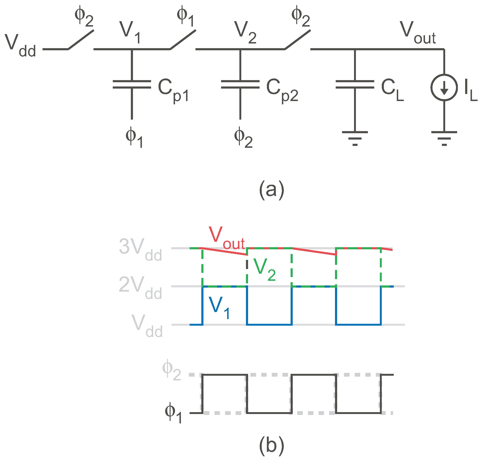
A simplified version of a charge pump is shown in
Figure 1a. By using alternating clock phases,
and
, a large voltage at the output can be generated, where each charge-pump stage adds an additional
to the output. The resulting output voltage is
where
N is the number of stages,
is the load current,
is the size of the pumping capacitor, and
f is the frequency of the clock. Between clock phases, the load current discharges the output voltage, which results in a ripple in the output voltage given by
where
is the capacitance loading the output node and
is the period of the ripple, which is established by the clock frequency. Depending on the load current, the size of the capacitors, and the clock frequency, this ripple can be significant.
From Equation (
2), increasing the load capacitance can reduce the ripple, but doing so comes at the expense of a longer rise time and a significant increase in the area consumed by the circuit. Often, a large off-chip capacitor is used to ensure a low-ripple output (e.g., [
7]). A number of designs have been introduced to help reduce the amount of ripple at the output while remaining fully integrated on-chip, with many of these designs focused on providing a low supply voltage for energy-harvesting applications [
8,
9]. The work in [
10] showed that, for high-voltage charge pumps (e.g.,
), the output ripple and efficiency of a charge pump can be improved by using complementary charge-pump structures, and simulated ripples of 65–73 mV were achieved. The charge pumps of [
11,
12] leveraged closed-loop structures to achieve ripple voltages in the tens-of-millivolts range; however, closed-loop operation does not guarantee low ripple voltages [
13,
14].
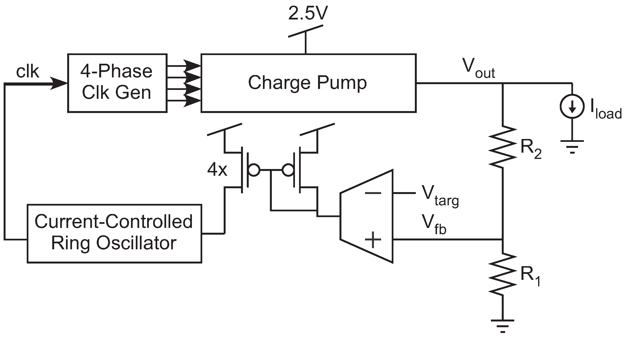
In [
5], we described a method to create a closed-loop charge pump that uses frequency regulation to help reduce the output ripple and still provide high output voltages. The circuit of [
5] is shown in
Figure 2. Due to the frequency regulation in the closed-loop structure, the output ripple value can be established by setting capacitor values, as described by
This structure was able to provide ripple voltages down to the tens-of-millivolt range for reasonably sized on-chip load capacitances [
5]. However, Equation (
3) shows that improving the ripple is inversely proportional to
. Therefore, to achieve very low output ripple (e.g., <1 mV), the load capacitance would become too large to integrate on-chip. For example, the charge pump of [
5] would require
≫ 1 nF for a ripple of 1mV, which would consume a considerable amount of chip real estate.
Our application of this low-ripple charge pump is to precisely program analog nonvolatile memory elements. Programming floating-gate (FG) transistors, which are the core elements in many nonvolatile memory arrays, requires elevated voltages to enable Fowler–Nordheim tunneling and hot-electron injection to modify the charge on the “floating” gate voltage [
15]. The amount of ripple provided by our charge-pump in [
5] was acceptable for the global erasure mechanism (Fowler–Nordheim tunneling), since precise programming in the erasure mode is not necessary. However, to accurately program FG devices to an exact amount of charge, the hot-electron injection voltages must be controlled extremely precisely [
16]. A key criteria for accurate programming of FG devices to a desired analog value is a precise voltage between the drain and the source. Using conventional programming techniques for analog floating-gate memories, such as [
15,
16,
17], this criteria results in the need of a very precise supply voltage for the FG devices with extremely low ripple (less than 1 mV).
One common method to reduce variation in a supply voltage is to use a voltage-regulator circuit. Since we are using the charge pump to create an elevated supply voltage that enables hot-electron injection, a voltage regulator after the charge pump should be able to attenuate the ripple significantly.
As a result, a voltage regulator could follow a simple open-loop charge pump (which has a very large output ripple). This technique has two major problems. First, it is hard to achieve ultra-low output ripple (less than 1 mV), because the ripple at the output of the charge-pump is so large and because the output voltage of an open-loop charge pump is highly dependent upon the load current, as shown in Equation (
1). Second, to be able to supply large-enough load currents, the output of an open-loop charge pump would have to be significantly high. Based upon simulations, in the case of our application, the charge-pump output voltage would need to be on the order of 20 V. This high voltage has a significant potential problem of stressing the devices in the voltage regulator, where high voltages across a single device can damage the junctions of the transistor.
Likewise, a closed-loop charge pump like
Figure 2 could be used to generate relatively low output ripple, and it can then be combined with a voltage regulator to further reduce the output ripple. The voltage regulator could either follow the closed-loop charge pump or be placed within the feedback loop of the charge pump. Regardless, the stability and phase margin of the voltage regulator are critical factors in ensuring that the overall output voltage meets the needs of programming analog nonvolatile memory. If the high voltage produced by the resulting circuit ever overshoots its final value, that excess voltage could significantly affect the accuracy of programming. Since the hot-electron injection process depends exponentially upon the drain-to-source voltage [
15], even a temporary overshoot of the desired supply voltage can result in drastic inaccuracies of programming analog nonvolatile memory. Since the elevated voltage for programming floating-gate transistors is only enabled when programming, the startup transients—particularly overshoot—are of critical importance.
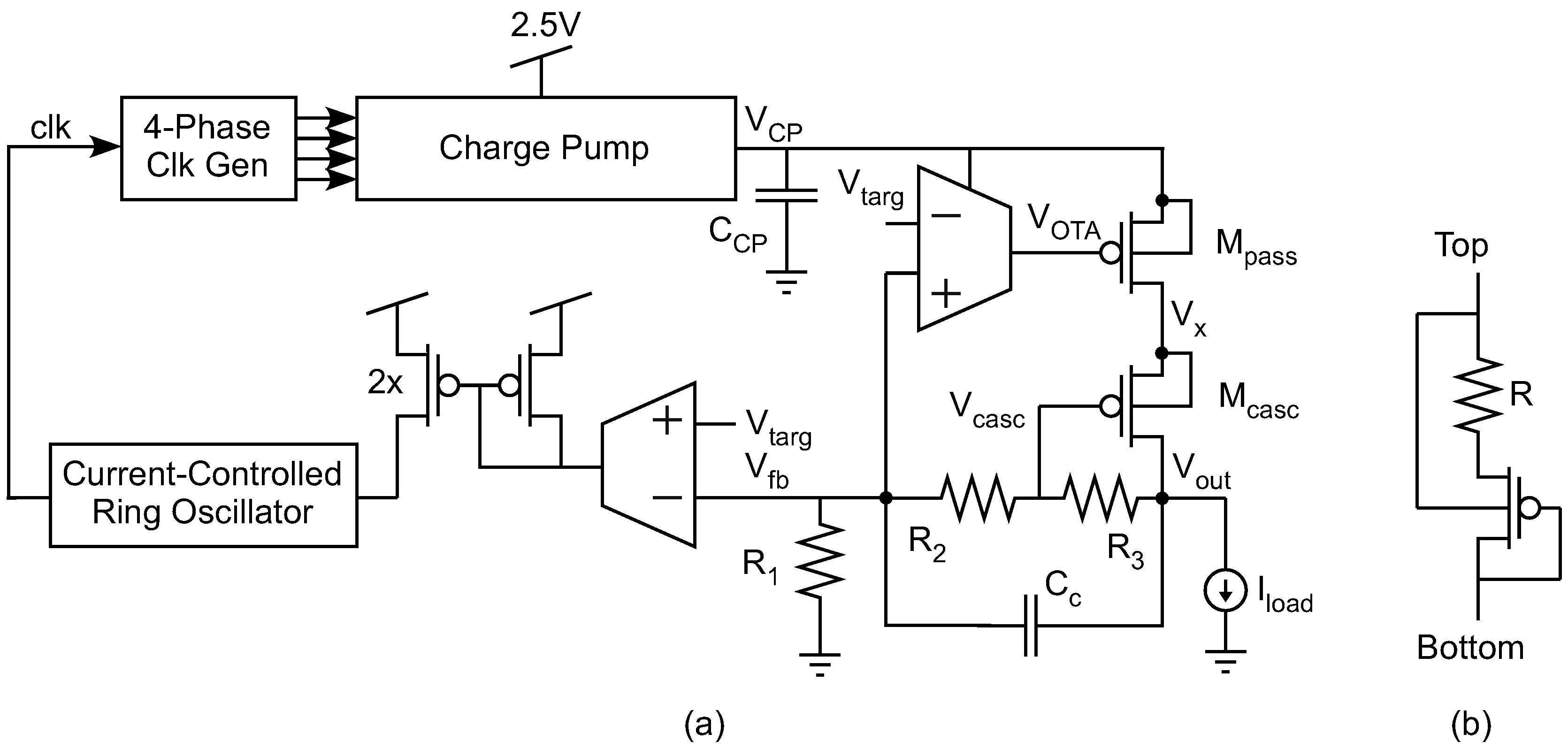
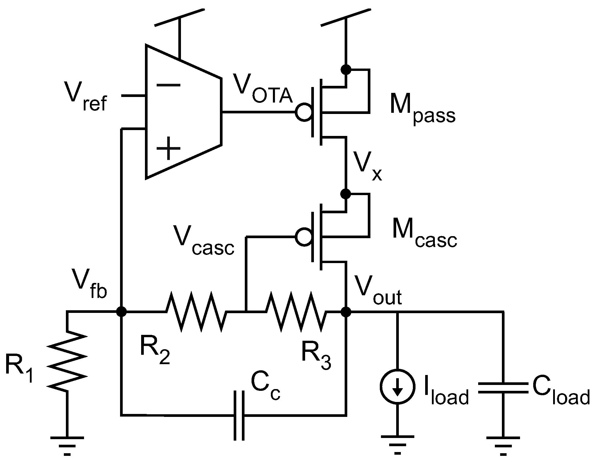
In this paper, we present a circuit in which a low-drop-out regulator is inserted inside the feedback loop of a closed-loop, variable-frequency charge pump. The block diagram of the proposed charge pump is shown in
Figure 3. This circuit is able to provide extremely low output ripple, and it can also be designed so that there is no possibility of overshoot of the output voltage, which will be discussed further in the frequency-stability discussion. Additionally, we present a method to self-bias a cascoded pass transistor in the voltage regulator, which helps improve the ripple suppression at the output.
Additional design considerations for the application of programming floating-gate transistors via hot-electron injection for analog applications are as follows. The exact voltage needed for hot-electron injection depends on the FG device being programmed. For a typical ∼7 nm gate-oxide device (i.e., 3.3 V device), which is the minimum oxide thickness required for long-term charge retention on an FG [
5], a source-to-drain voltage of approximately >5 V is required for reasonably fast programming via hot-electron injection [
6,
16]. However, the programming support circuitry in many floating-gate programming systems for analog applications requires additional voltage overhead, so the charge pump must be able to accommodate higher output voltages. In the system of [
18], a voltage of 6.5 V is typically used. The required output current of the charge pump is modest, but it needs to be able to handle changing current values as the devices are programmed. In the programming system of [
18], the charge pump needs to supply the programming support circuitry in addition to the FG transistors, themselves, and the maximum current is approximately 20
A. Of note, the elevated voltages are only needed on an infrequent basis. Since the purpose of many programmable analog systems is for trimming, offset removal, bias current generation, and other values that require a static amount of charge on the floating gate [
19], the charge pump used for providing injection voltages will only be turned on “as needed” for programming, which is likely an infrequent occurrence (e.g., daily, monthly, or yearly) and for a short period of time (approximately one second). Accordingly, high efficiency is not a critical need for this particular charge-pump application.
4. Measurement Results
The complete charge pump was designed and fabricated in a 0.35
m standard CMOS process with device sizes given in
Table 1. The rated supply voltage for this process is 3.3 V, and the chip supply voltage is regulated down to 2.5 V for the operation of the charge pump (as well as the floating-gate transistors and their supporting circuitry). The die area of this circuit is 504
m × 324
m. The die photo of the proposed charge pump is shown in
Figure 8. Both differential amplifiers used in this circuit are conventional 5-transistor OTAs.
A Tektronix MSO4054 Mixed-Signal Oscilloscope (500 MHz) was used to measure the output voltage. The supply voltage and the target voltage were provided by an Agilent E3631A Programmable DC Power Supply. The load current was set by a custom off-chip current sink and was verified by a Keithley 6485 Picoammeter.
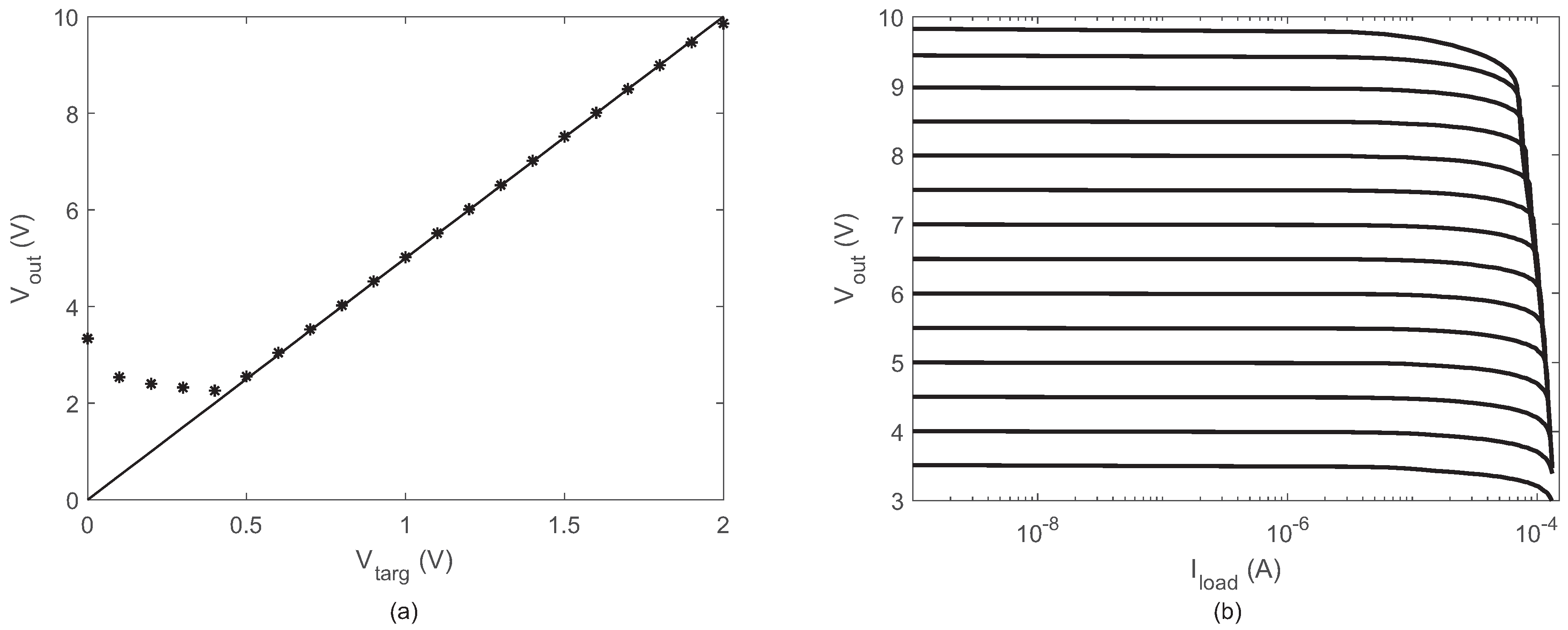
Figure 9a shows the measured transfer curve from
to
. The slope of this curve is 5, which shows that the charge pump can generate a high voltage equal to
. Deviation from the ideal line at the low voltages is because the input transistors of the OTAs drop out of saturation with low
; however, since the charge pump only needs to supply voltages greater than the supply voltage, the transfer characteristic does not need to follow the ideal slope of 5
for
V, thereby significantly relaxing the requirements of the OTA designs. Deviation at high voltages is caused by the limitations imposed on the cascode transistors described by Equations (
4) and (
5).
Figure 9b shows the closed-loop load regulation of the proposed charge pump for multiple output voltages, which were set by changing the value of
. The hot-electron injection process of floating-gate transistors requires that the voltage generating the injection conditions be constant with a range of load currents [
16,
18], and
Figure 9b indicates that this circuit is capable of providing a consistent output voltage under varying load currents.
A typical value for an injection voltage in a 0.35
m standard CMOS process is 6.5 V [
6].
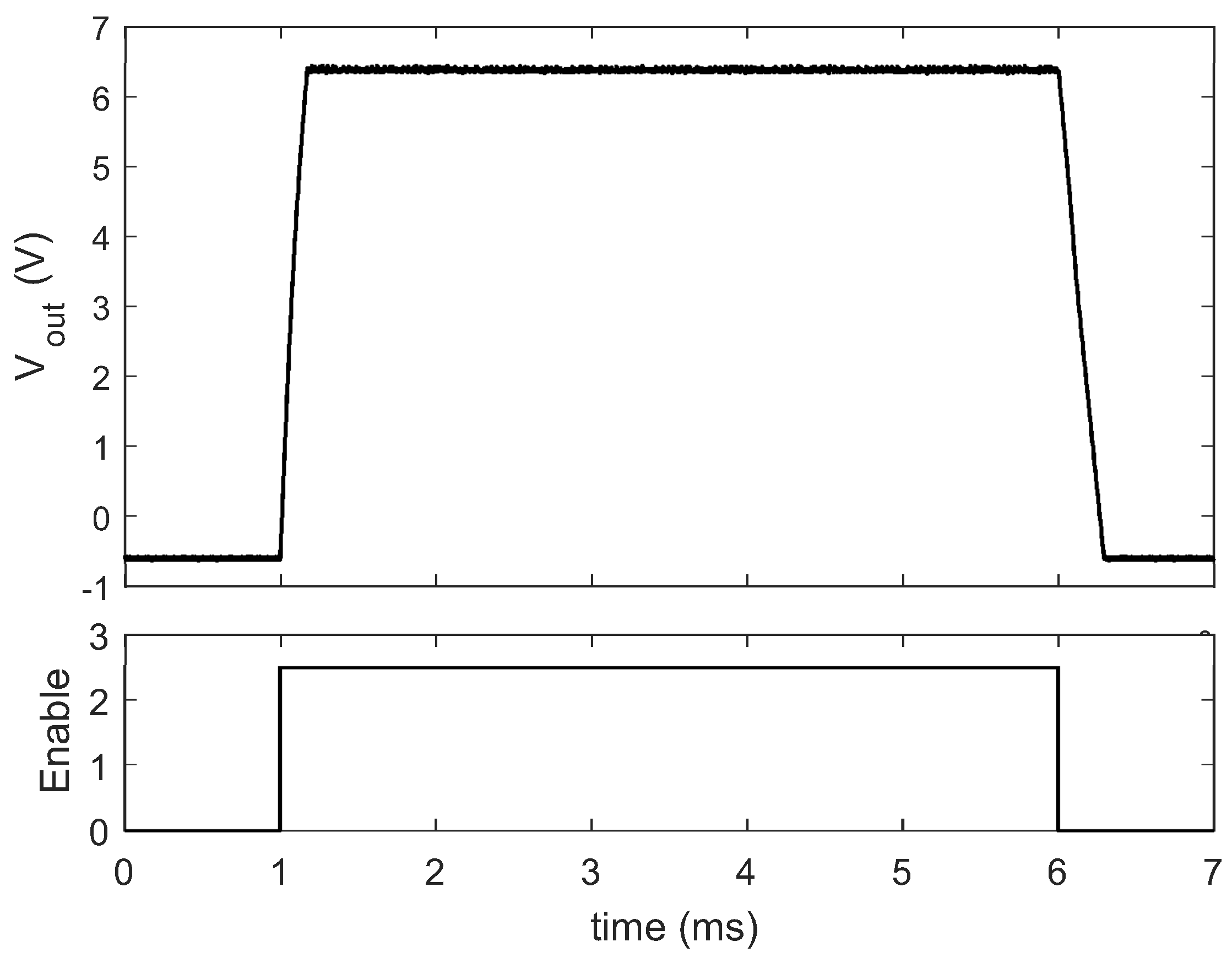
Figure 10 shows the measured transient response for a typical programming pulse. The charge pump is enabled and disabled, with a steady-state output voltage of 6.5 V while loaded with a 40
A load current and an approximately 80 pF load capacitance. The output reaches steady-state conditions in less than 0.2 ms. According to our measurements, the output voltage of the proposed charge pump under different load currents converges to
with a behavior that is between critically damped and over-damped, meaning that there is no overshoot. Preventing overshoot is critical in floating-gate programming applications where a small change in the voltage can seriously impact the accuracy of programming.
The current consumption of the proposed charge pump is 0.73 mA and 1.2 mA for no load and 100
A of load, respectively. The efficiency of a charge-pump is the ratio of the power delivered by the charge pump to the power supplied to the charge pump, as described by
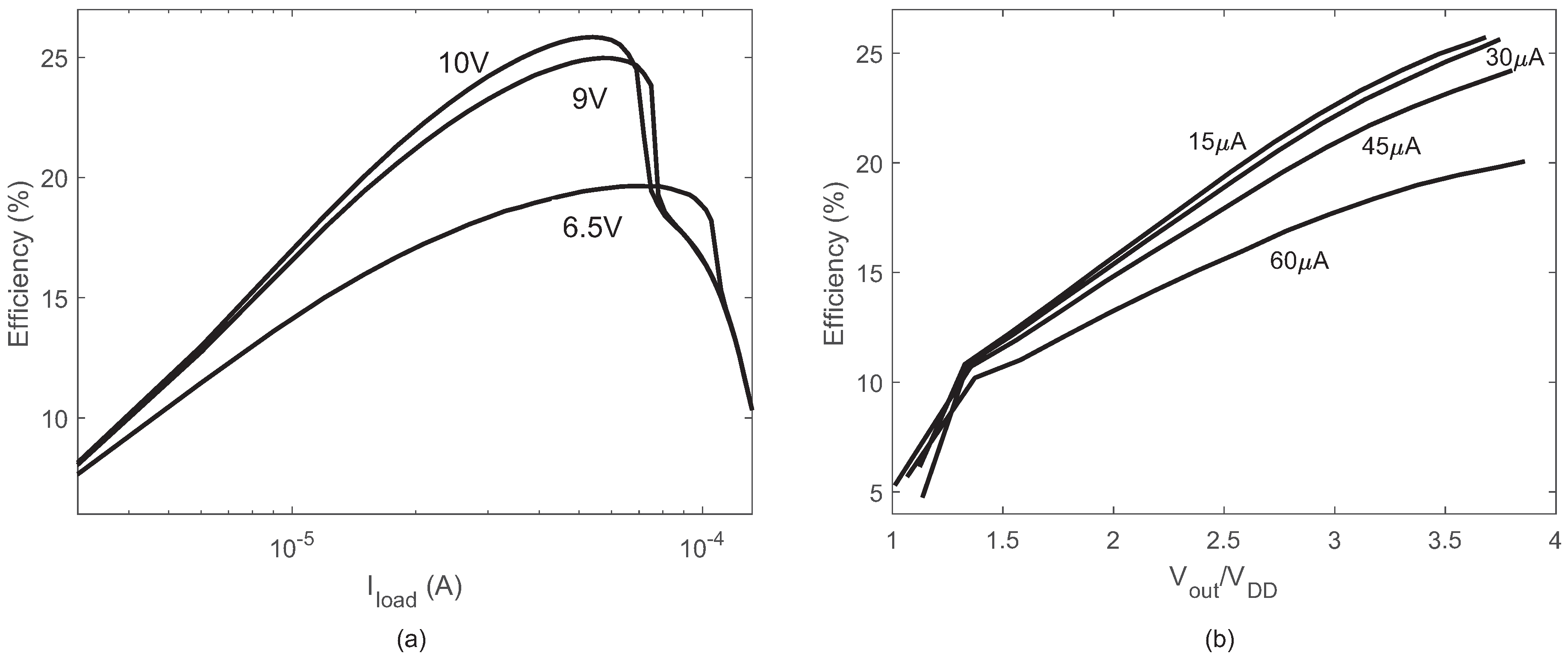
The measured efficiency of this circuit is shown in
Figure 11a for output voltages of 6.5, 9, and 10 V and varying load currents. The maximum efficiency is 25.7% and is for the 10 V output case. The measured efficiency is also shown for various step-up ratios (
) and load currents in
Figure 11b. As also indicated by
Figure 11, the charge pump provides better efficiency for higher step-up ratios. However, a low efficiency number is not an issue in the charge pumps used for floating-gate programming because the charge pump is only enabled for a short period of time while programming the floating-gate transistors; otherwise, the charge pump is disabled.
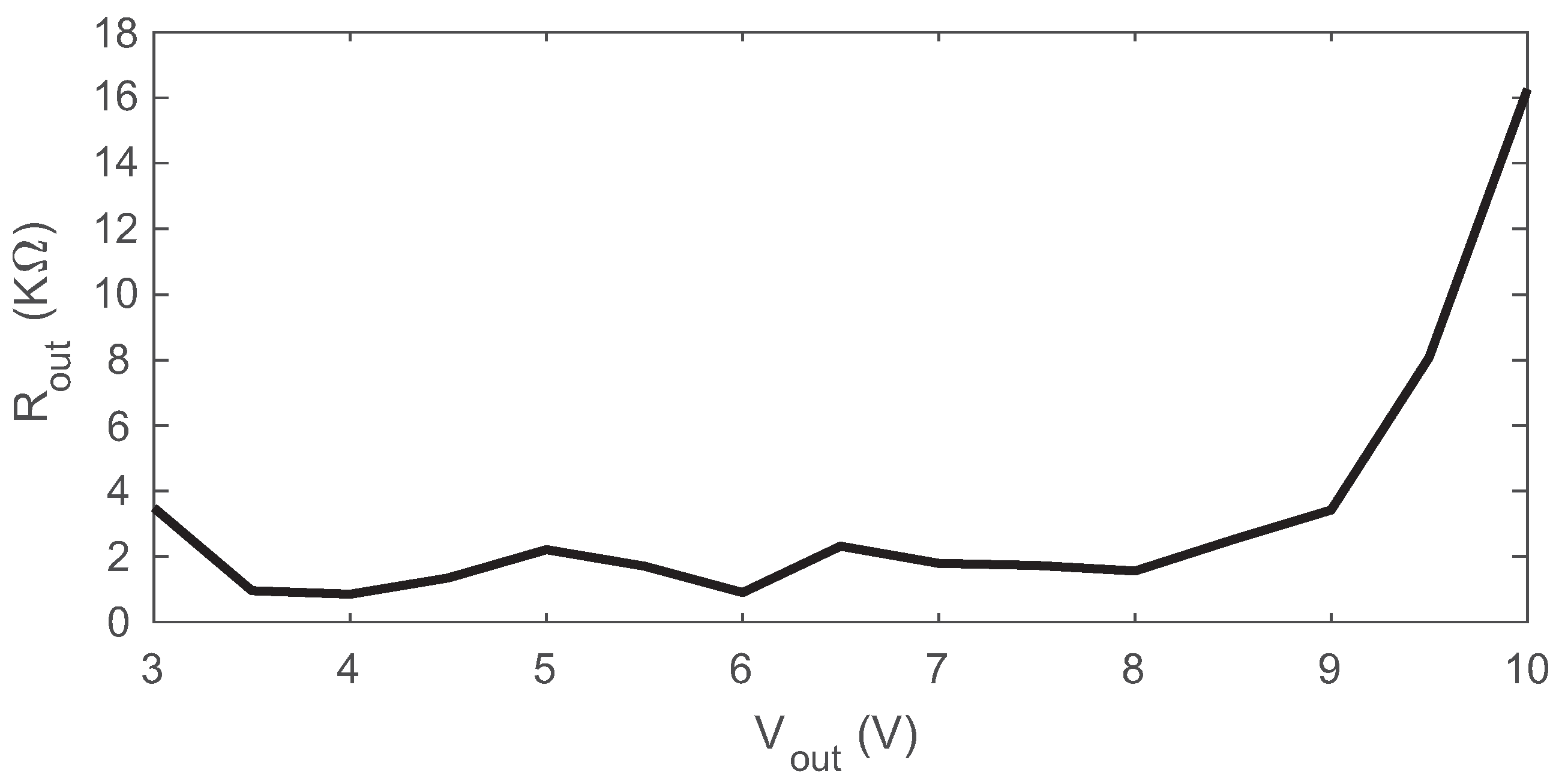
The output impedance of the proposed charge pump with
A for different output voltages is shown in
Figure 12. The output resistance (
) stays under 4 k
for a wide range of output voltages.
begins to increase when
V because the loop gain of the system reduces with very-high output voltages.
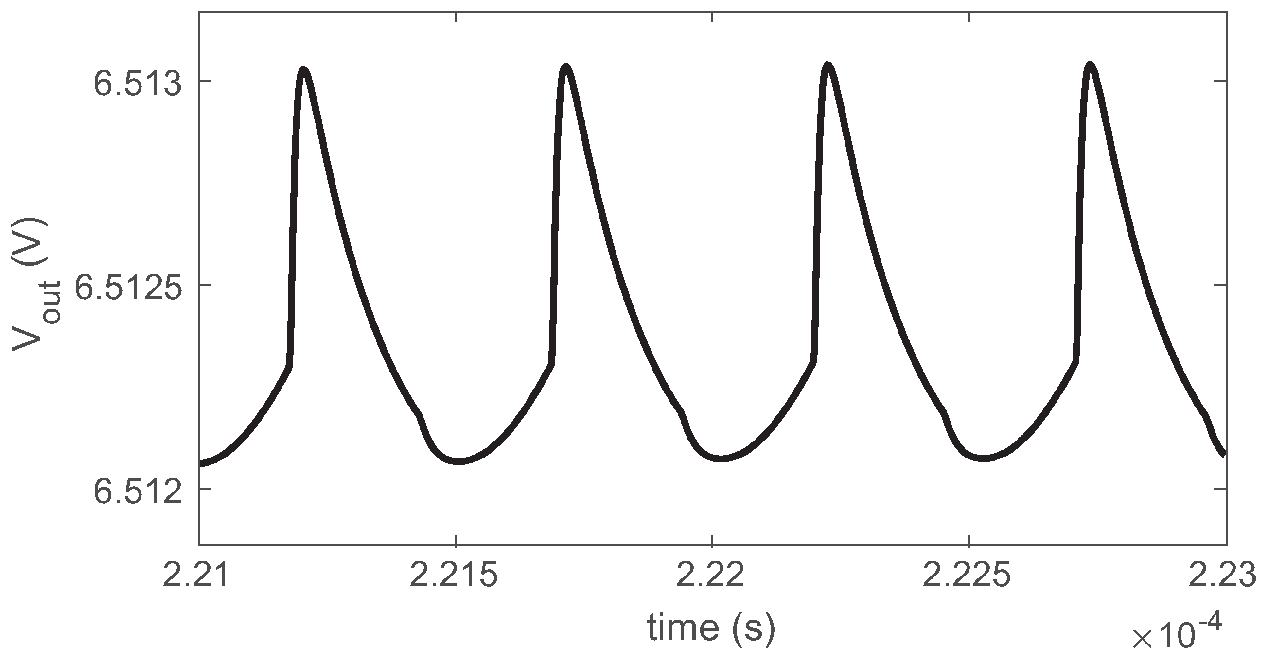
The amount of ripple at the output can have a significant impact on the accuracy of programming floating-gate transistors. As can be seen from
Figure 10, the ripple on the output voltage is very small. Because the ripple was smaller than the limits of our measurement equipment (i.e., within the quantization noise), we leveraged RC-extracted simulations under similar conditions as our experimental setup of
Figure 10 to determine the amount of ripple. The RC-extracted simulation results are shown in
Figure 13 with
V,
pF, and
A.
Figure 13 shows that the output ripple was approximately 1mV, which is sufficiently low for our analog nonvolatile memory programming application. Of note, this load capacitance is small enough that it can easily be integrated on-chip, and even larger integrated capacitances could be used to further reduce the ripple. Furthermore, these results show the effectiveness of the charge-pump-LDO loop combination; even the relatively low output ripple of the variable-frequency charge pump of [
5] would have required
nF to achieve sub 1mV ripple, which is far too large to integrate on-chip in most applications. The LDO in the loop reduces the necessary load capacitance by several orders of magnitude.
Table 2 shows a comparison of the proposed charge pump with other published charge pumps. Specifically, we included other regulated charge pumps in this table that (1) were fabricated, (2) provide
>
for the process, (3) do not utilize a large off-chip capacitor to reduce the ripple, and (4) have a reported ripple voltage less than 100 mV. Of the reported charge pumps that meet the above criteria as shown in
Table 2, our proposed charge pump is capable of the lowest ripple.
Comparing this new charge pump to our previous work [
5], approximately half of the increase in size is due to the larger pumping capacitors that were used to increase the current-driving capabilities. The rest of the area was due to the size of the LDO and the resistive divider, which included drawn resistors instead of only diode-connected pFETs as in [
5]. This new charge pump is capable of an order-of-magnitude lower ripple voltages. However, the inclusion of the LDO prevents the entire circuit from generating as high voltages as in [
5]; the circuit of [
5] was specifically designed to be able to achieve high voltages without subjecting any transistor to voltage drops greater than
and ensuring that no junction undergoes a breakdown voltage. However, the OTA in the LDO limits the output voltage to 10 V.
Both [
11,
12] would be capable of providing the voltages necessary for programming FG transistors via hot-electron injection if no significant voltage overhead is required for the programming circuitry, and they both provide larger current-driving capabilities than the proposed charge pump. However, their ripple is larger, and they consume considerably larger real estate. The circuit of [
22], on the other hand, is very compact. However, while it is able to produce a voltage that is large-enough for injection, the maximum load current is quite small and would likely be limiting to FG programming applications. Even though the circuit of [
23] was fabricated in a 65 nm process with a significantly reduced supply voltage, FG devices require a gate oxide of ∼7 nm for long-term retention [
5], which sets the voltages necessary for inducing hot-electron injection. The maximum voltage of [
23] is not sufficient for FG programming.
In summary, of the circuits listed in
Table 2, the proposed charge pump is the best suited to meeting the needs of precision programming of analog components via hot-electron injection. If the floating-gate transistors were instead being used for digital memory, many other high-voltage charge pumps would be capable of providing the elevated voltages needed; since the charge on the FG of a digital device does not need to be as precisely controlled, charge pumps with larger ripples would suffice [
14,
24,
25], and even open-loop charge pumps with output voltages that are much more dependent on the load current (see Equation (
1)) could be used [
26,
27,
28]. The high accuracy needs of the analog memory necessitates more-stringent requirements of the charge pump.


