LDMOS versus GaN RF Power Amplifier Comparison Based on the Computing Complexity Needed to Linearize the Output


Abstract
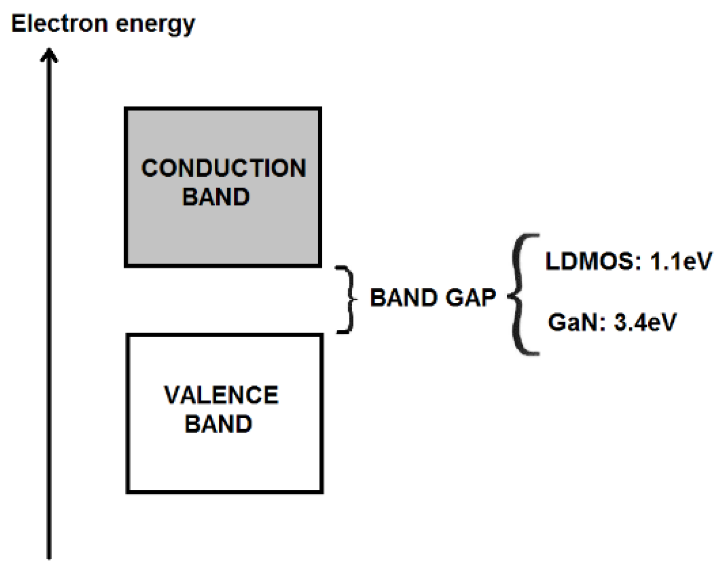
:1. Introduction
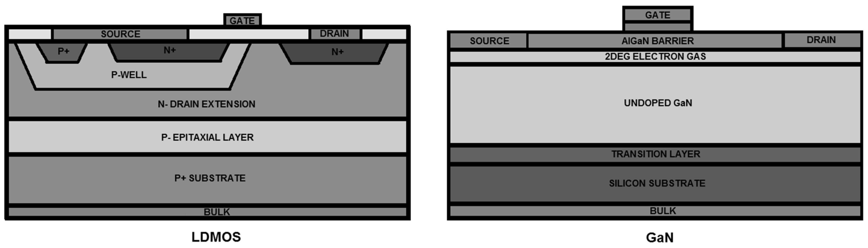
2. Materials and Methods
- -
- PD57006S-E: an LDMOS amplifier manufactured by ST Microelectronics, with the following characteristics:
- -
- Output power: 5 W
- -
- Power supply: 28 V
- -
- Gain: 14.8 dB
- -
- Efficiency: 50%
- -
- NPTB00004A: a GaN amplifier manufactured by MACOM, with the following characteristics:
- -
- Output power: 6 W
- -
- Power supply: 28 V
- -
- Gain: 15 dB
- -
- Efficiency: 62%
3. Results
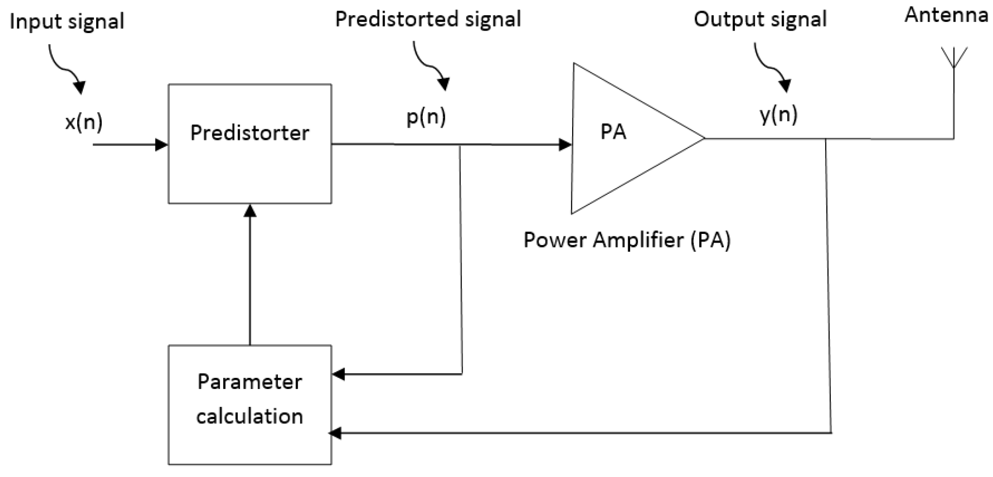
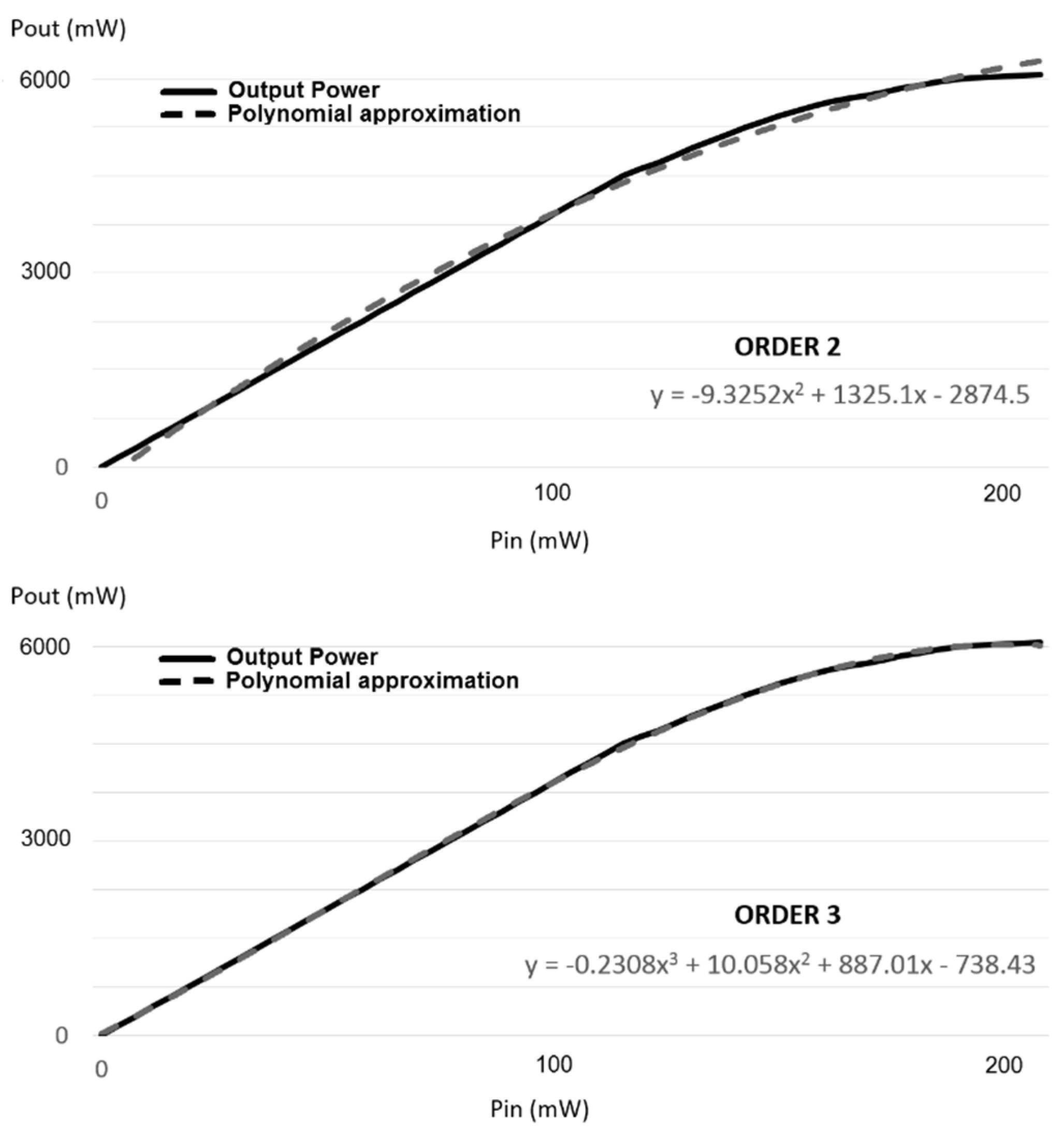
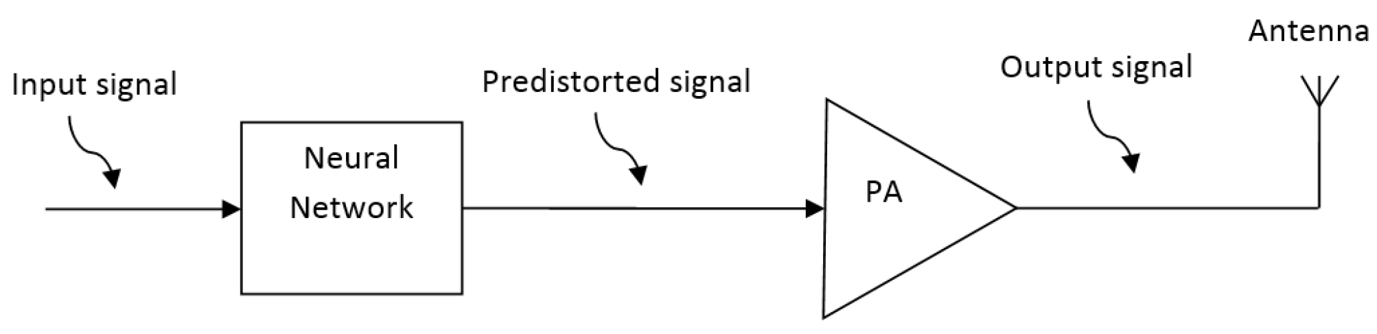
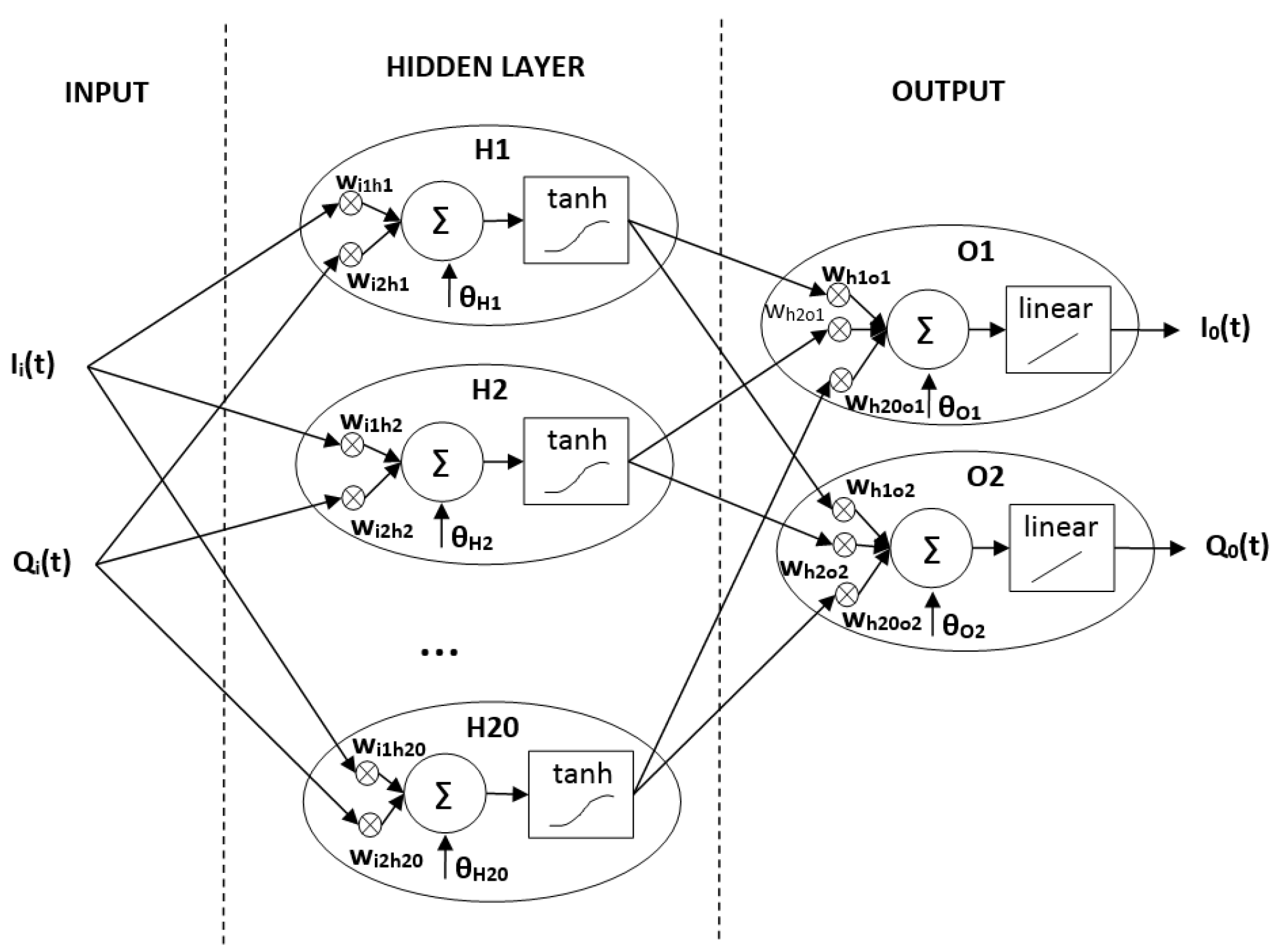
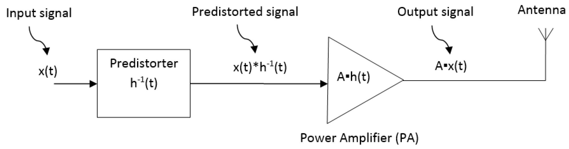
3.1. Predistortion Technique
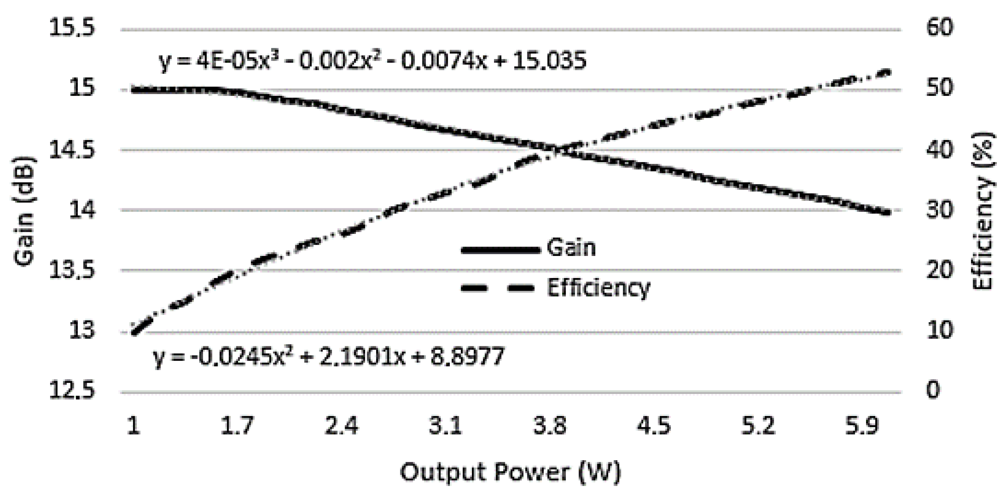
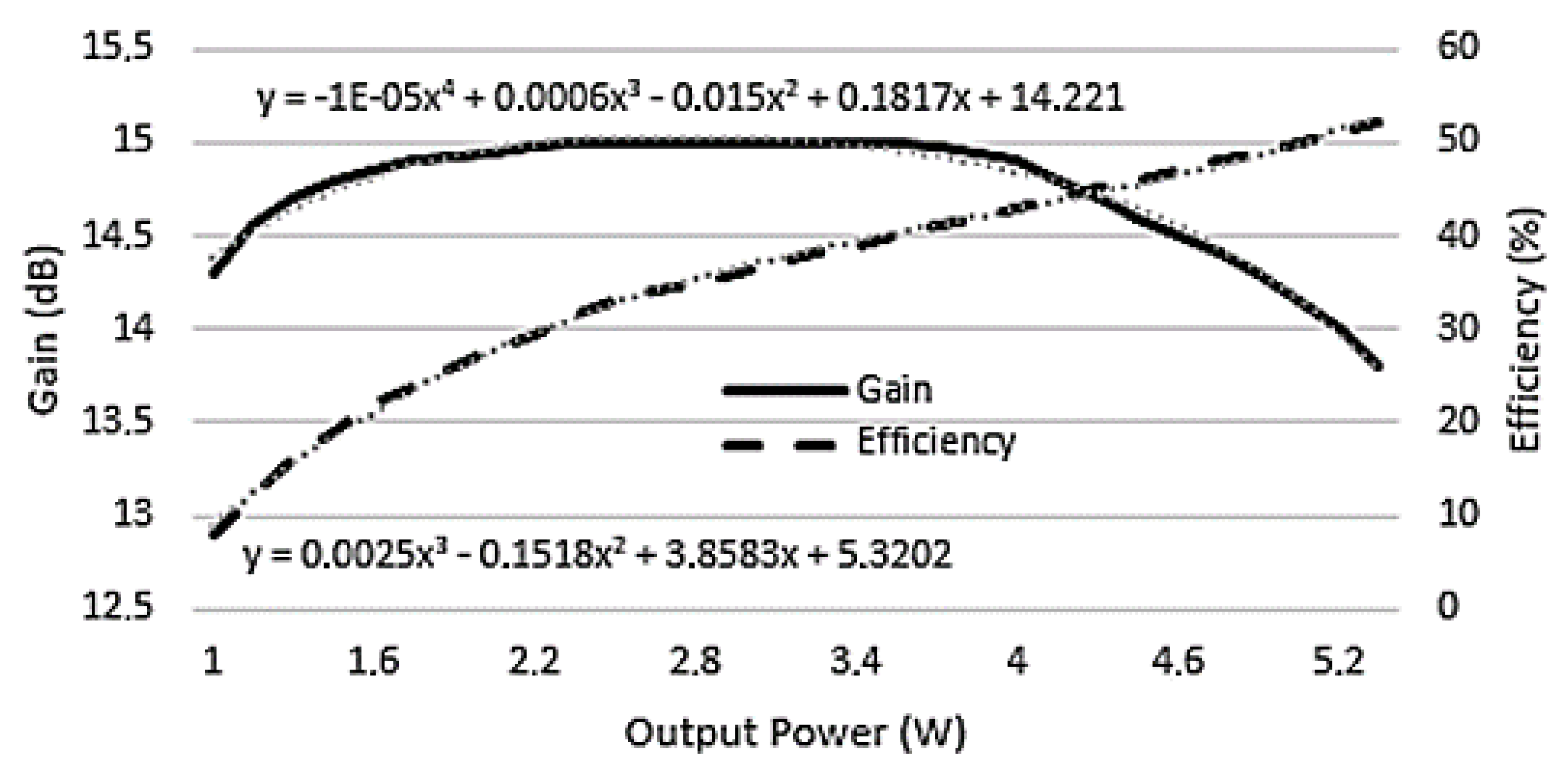
3.2. LDMOS versus GaN Power Amplifiers
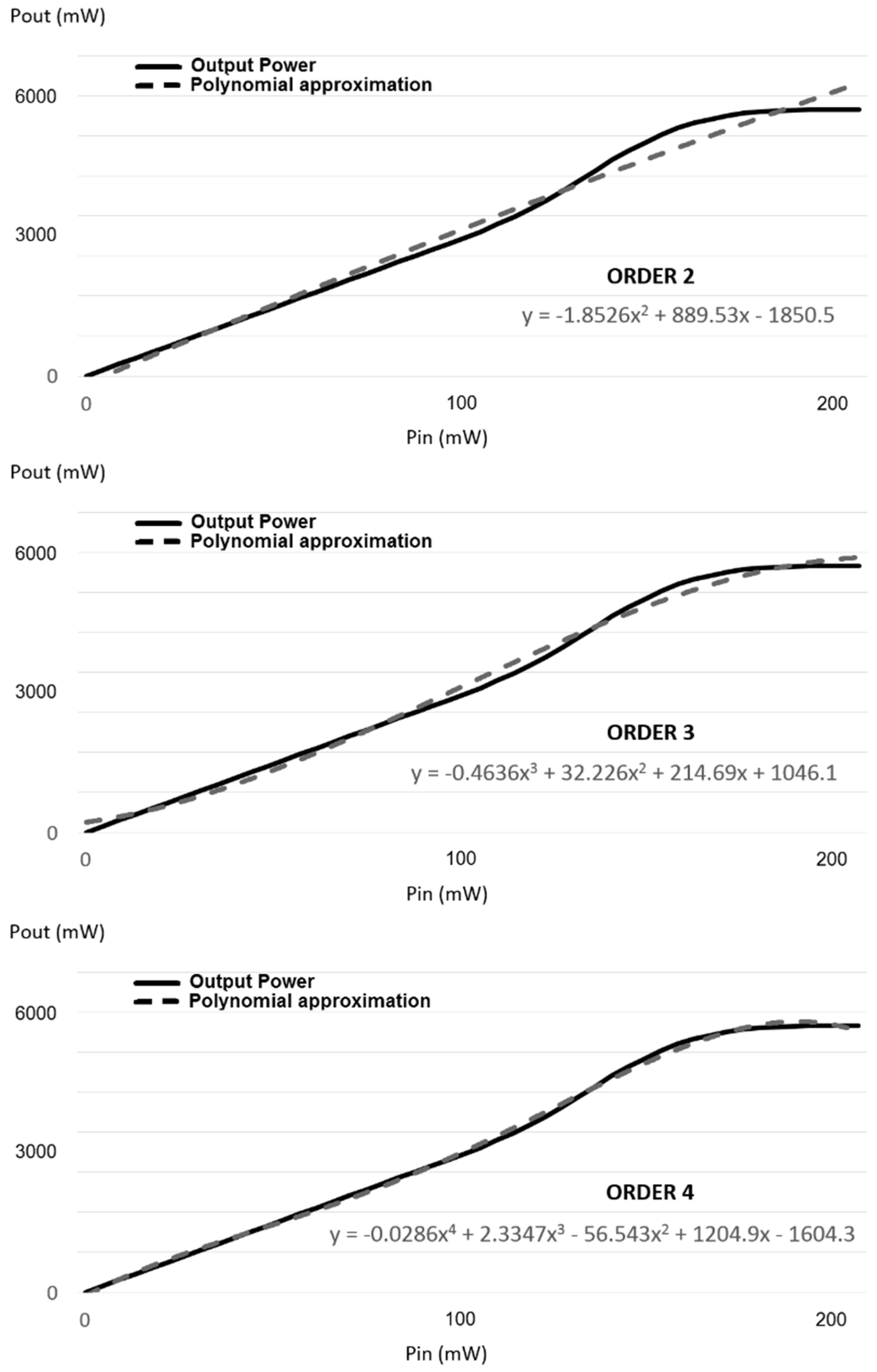
3.3. Complexity Analysis of the Linearization System (LDMOS vs. GaN)
3.4. Power Amplifier Complexity Comparison
4. Discussion
Author Contributions
Funding
Acknowledgments
Conflicts of Interest
References
- Kenington, P.B. High-Linearity RF Amplifier Design; Artech House: Norwood, MA, USA, 2000. [Google Scholar]
- Yu, H.; El-Sankary, K.; El-Masry, E.I. Distortion Analysis Using Volterra Series and Linearization Technique of Nano-Scale Bulk-Driven CMOS RF Amplifier. IEEE Trans. Circuits Syst. Regul. Pap. 2015, 62, 19–28. [Google Scholar] [CrossRef]
- Morgan, D.R.; Ma, Z.; Kim, J.; Zierdt, M.G.; Pastalan, J. A Generalized Memory Polynomial Model for Digital Predistortion of RF Power Amplifiers. IEEE Trans. Signal Process. 2006, 54, 3852–3860. [Google Scholar] [CrossRef]
- Gilabert, P.; Montoro, G.; Bertran, E. On the Wiener and Hammerstein models for power amplifier predistortion. In Proceedings of the 2005 Asia-Pacific Microwave Conference Proceedings, Suzhou, China, 4–7 December 2005. [Google Scholar] [CrossRef]
- Ai, B.; Yang, Z.-X.; Pan, C.-Y.; Tang, S.-G.; Zhang, T.-T. Analysis on LUT Based Predistortion Method for HPA with Memory. IEEE Trans. Broadcast. 2007, 53, 127–131. [Google Scholar] [CrossRef]
- Mkadem, F.; Boumaiza, S. Physically Inspired Neural Network Model for RF Power Amplifier Behavioral Modeling and Digital Predistortion. IEEE Trans. Microwave Theory Tech. 2011, 59, 913–923. [Google Scholar] [CrossRef]
- Jiménez, V.P.G.; Jabrane, Y.; Armada, A.G.; Said, B.A.E.; Ouahman, A.A. High Power Amplifier Pre-Distorter Based on Neural-Fuzzy Systems for OFDM Signals. IEEE Trans. Broadcast. 2011, 57, 149–158. [Google Scholar] [CrossRef]
- Moritz, R.; Leung, H.; Huang, X. Nonlinear Compensation for High Power Amplifiers using Genetic Programming. In Proceedings of the 2007 IEEE International Symposium on Circuits and Systems, New Orleans, LA, USA, 27–30 May 2007; pp. 2323–2326. [Google Scholar]
- Nuttinck, S.; Gebara, E.; Laskar, J.; Rorsman, N.; Olsson, J.; Zirath, H.; Eklund, K.; Harris, M. Comparison between Si-LDMOS and GaN-based microwave power transistors. In Proceedings of the IEEE Lester Eastman Conference on High Performance Devices, Newark, DE, USA, 8 August 2002; pp. 149–154. [Google Scholar]
- Nunes, L.C.; Cabral, P.M.; Pedro, J.C. Am/am and am/pm distortion generation mechanisms in si ldmos and gan hemt based rf power amplifiers. IEEE Trans. Microwave Theory Tech. 2014, 62, 799–809. [Google Scholar] [CrossRef]
- Yusoff, Z.; Akmal, M.; Carrubba, V.; Lees, J.; Benedikt, J.; Tasker, P.J.; Cripps, S.C. The benefit of GaN characteristics over LDMOS for linearity improvement using drain modulation in power amplifier system. In Proceedings of the IEEE 2011 Workshop on Integrated Nonlinear Microwave and Millimetre-Wave Circuits, Vienna, Austria, 18–19 April 2011; pp. 1–4. [Google Scholar]
- ETSI EN 300 394-1 V3.3.1 (2015-04). Terrestrial Trunked Radio (TETRA); Conformance Testing Specification; Part1: Radio. Available online: https://www.etsi.org/deliver/etsi_en/300300_300399/30039401/03.03.01_60/en_30039401v030301p.pdf (accessed on 15 April 2015).
- Sáez, R.G.; Marqués, N.M. RF Power Amplifier Linearization in Professional Mobile Radio Communications Using Artificial Neural Networks. IEEE Trans. Ind. Electron. 2019, 66, 3060–3070. [Google Scholar] [CrossRef]
- Haykin, S. Neural Networks and Learning Machines, 3rd ed.; Prentice-Hall: Upper Saddle River, NJ, USA, 2009. [Google Scholar]


| LDMOS | GaN | |
|---|---|---|
| Maximum frequency | 22 GHz | 30 GHz |
| Power density | 2 W/mm | 10 W/mm |
| Efficiency at P1dB | 60% | 70% |
| Bandwidth | 500 MHz | 2500 MHz |
| Maximum temperature | Lower | Higher |
| Breakdown voltage | Lower | Higher |
| Maximum operating voltage | Lower | Higher |
| Cgs | Higher | Lower |
| Cds | Higher | Lower |
| Rin | Lower | Higher |
| Rout | Lower | Higher |
| Maximum RF power | 1.5 kW | 1 kW |
| Price | Lower | Higher |
| Robustness against impedance mismatches | Higher (65:1) | Lower (20:1) |
| LDMOS (PD57006S-E) | GaN (NPTB00004A) |
|---|---|
| NTPB00004A | PD57006S-E | |
|---|---|---|
| Output 1dB compression point (P1dB) | 36.5 dBm | 37.5 dBm |
| Output Power @ 925 MHz | 35 dBm | 36 dBm |
| Efficiency @ Output Power | 50% | 40% |
| ACP improvement | 12 dB | 10.5 dB |
| Number of Neurons | ACP Improvement |
|---|---|
| 20 | 10.5 dB |
| 30 | 11 dB |
| 40 or more | 11.2 dB |
| Neurons in 1st Hidden Layer | Neurons in 2nd Hidden Layer | ACP Improvement | |
|---|---|---|---|
| NTPB00004A | 20 | - | 12 dB |
| PD57006S-E | 18 | 6 | 12 dB |
| GaN | LDMOS | |
|---|---|---|
| Number of cycles to linearize with the neural network | 6500 | 8500 |
| Necessary DSP frequency to linearize in 15 ms | 456 MHz | 608 MHz |
© 2019 by the authors. Licensee MDPI, Basel, Switzerland. This article is an open access article distributed under the terms and conditions of the Creative Commons Attribution (CC BY) license (http://creativecommons.org/licenses/by/4.0/).
Share and Cite
Gracia Sáez, R.; Medrano Marqués, N. LDMOS versus GaN RF Power Amplifier Comparison Based on the Computing Complexity Needed to Linearize the Output. Electronics 2019, 8, 1260. https://doi.org/10.3390/electronics8111260
Gracia Sáez R, Medrano Marqués N. LDMOS versus GaN RF Power Amplifier Comparison Based on the Computing Complexity Needed to Linearize the Output. Electronics. 2019; 8(11):1260. https://doi.org/10.3390/electronics8111260
Chicago/Turabian StyleGracia Sáez, Raúl, and Nicolás Medrano Marqués. 2019. "LDMOS versus GaN RF Power Amplifier Comparison Based on the Computing Complexity Needed to Linearize the Output" Electronics 8, no. 11: 1260. https://doi.org/10.3390/electronics8111260
APA StyleGracia Sáez, R., & Medrano Marqués, N. (2019). LDMOS versus GaN RF Power Amplifier Comparison Based on the Computing Complexity Needed to Linearize the Output. Electronics, 8(11), 1260. https://doi.org/10.3390/electronics8111260