1. Introduction
Nowadays, it is necessary to find some alternatives to test power electronic converters to reach more advantages over the classical test flow which only includes off-line simulations followed by tests in a real prototype. Off-line simulation is the cheapest and safest possibility to test a power electronic system especially for the initial phase of testing. However, off-line simulation is not enough for guaranteeing a proper behavior of the final hardware implementation so tests with both the real controller and power converter are necessary. However, before testing both the final controller and power converter together, other intermediate steps are possible, which can accelerate the process, and also decrease the risk of managing real power [
1] when testing the final controller. In the past, to test a more realistic model of the controller, which is digital in many cases, than just a transfer function or high-level model, some simulation alternatives appeared. For example, mixed-signal simulators [
2], a mixture of VHDL (Very high-speed integrated circuit Hardware Description Language) and analog signal extension (VHDL-AMS simulator) [
3], or using two different simulators, one for the controller part which usually designs in VHDL and the other one for the analog power converter part [
4], were employed to tackle this issue. However, these simulation alternatives were not trivial in many cases, they were usually very slow and, above all, did not meet the requirement of testing the real final controller in hardware.
Recently, it has been possible to emulate controllers and power converters in real-time (RT), which is known as HIL (Hardware-In-the-Loop), regardless of whether the controller is analog or digital. A comprehensive study on simulation versus HIL alternatives for power converters is accomplished in [
5]. In HIL testing, the power converter is replaced by an emulation of it to mimic the real converter and it is made to interact with the real controller to test the controller. HIL model is closer to the actual real system; it saves money, especially in the case of testing expensive systems; allows tests without damaging the real system; and saves a lot of efforts during the implementation of a design [
6,
7,
8,
9,
10,
11,
12,
13,
14,
15,
16,
17,
18,
19,
20].
Because of the rapid progress of semiconductors, the switching frequency of the power converter is increasing. Precise modeling of switched-power converter needs an integration step at least 100 times less than its switching period. The minimum integration step of the microprocessor-based HIL implementations, which were used traditionally was about hundreds or tens of
s that is not small enough for high-frequency applications [
21]. FPGAs (Field Programmable Gate Array) have resulted in a revolution of HIL systems because they make it possible to test a digital model of a mid-high switching frequency power converter in RT (it was nearly impossible by using microprocessors) and they also have excellent parallel processing capabilities and small bus latencies that make them ideal for fast RT simulation [
4,
22,
23,
24,
25,
26,
27,
28,
29,
30]. HDL (Hardware Description Language) models of power converters can be emulated in an FPGA if the model is synthesizable to make it faster in comparison with microprocessor-based HIL implementations [
31,
32]. Recently, HIL systems which use FPGAs can emulate complex power converters with an integration step about 1
s or lower without requiring optimization [
33]. However, simple and optimized models implemented in FPGA can reach integration steps under 100 ns [
31,
32,
34].
Different numerical formats used in FPGA-based HIL systems play a crucial role in needed hardware resources, the minimum achievable clock frequency, the design time, and the accuracy of the model. A comparison between fixed-point and floating-point representation is done in [
5,
31], in which FPGA-based HIL systems were proposed. The results confirmed that floating-point representation needs more hardware resources and it is not as fast as fixed-point (up to 10 times more resources and slower) but the effort design is less and the resolution is optimized in different calculations. This is why most HIL applications use floating-point representation [
35]. In fixed-point representation, the designer has to define the widths of the signals to provide an optimized model, which is much faster and needs fewer hardware resources [
5,
31]. It is important to highlight that, even using FPGAs, HIL models remain simple compared with electrical simulators. In many cases, they do not consider any losses because that would make the model slower and may not reach RT. However, it is clear that including some losses would make the model much more accurate.
This paper proposes three different models of the full-bridge converter with and without considering losses based on different possible numerical formats. It will prove that considering losses results in more accurate results even if it makes the models more complex which results in increasing the RT simulation step. The HIL model of the full-bridge is implemented in three different versions: using floating-point representation, using fixed-point representation without taking into account the characteristics of FPGA embedded DSP (Digital Signal Processors) blocks, and optimized fixed-point. The main purpose of this paper is to quantify the differences between these three proposed models and to compare different possibilities of implementation. However, hardware implementation of different numerical formats to solve differential equations presents some issues when they are applied to power electronic converters, which are explained in detail. Furthermore, this paper explores using the idea that, by limiting the width of signals to those of the embedded DSP blocks in FPGAs, the model can achieve smaller simulation step, which results in reaching a more accurate model.
In this paper, initially, a full-bridge converter is presented as an application example with and without considering losses. In
Section 2, the equations of the model are calculated by using an explicit Euler approach, and three different possibilities to model a power converter are discussed. In
Section 3, the reference model, float model, non-optimized fixed-point model (nOFPM), and OFPM are proposed by using different numerical formats. The implementation of the full-bridge model is also presented and the schematic of the model is discussed in detail. The benefits of the optimized model are confirmed by several experimental and simulation results in
Section 4. Finally, conclusions are given in
Section 5.
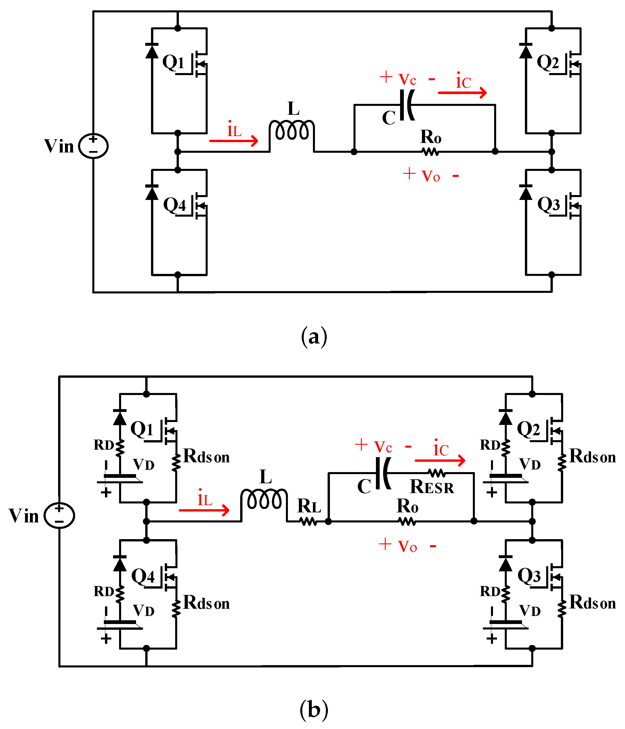
3. Implementation
The implementation of the full-bridge is explained in this section. Three different implementations have been developed using real type, float type, and fixed point numerical format. The simplest approach is using the real type, which allows translating the equations directly into VHDL. It can be implemented by using Equations (
5)–(
7). However, as mentioned above, the real numerical format is not synthesizable, and it cannot be used in a real-time FPGA implementation, thus it is used only as a reference model for simulation. Real numerical format uses
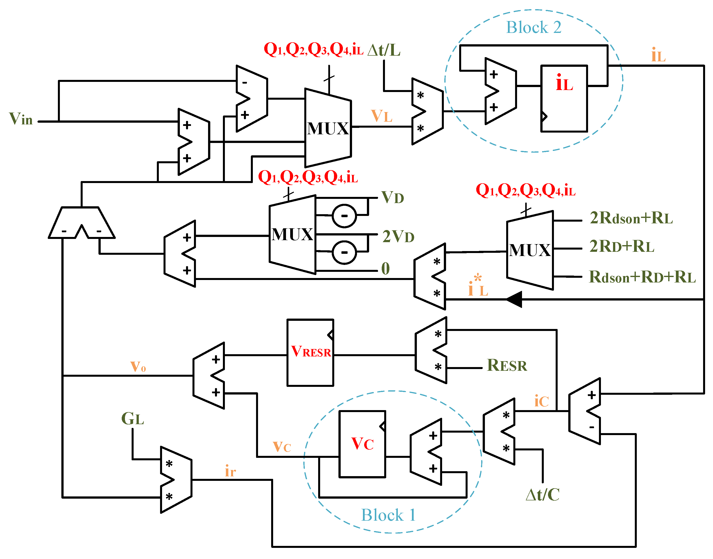
IEEE-754 double precision standard (64-bits) with a mantisa field of 53 bits. Using this numerical format, numeric resolution problems are avoided because of the high number of signal bits, thus it is the best choice as the reference model to have a comparison between different approaches. In this paper, the real numerical format with a time step of 1 ns is used as the reference model. The schematic of the Full-bridge model without considering the variable width is shown in
Figure 2. This schematic is the result of translating Equations (
5)–(
7) into VHDL and using real type.
The model has three outputs,
,
, and
, and some inputs:
,
, switches states, the forward voltage of the diode, the resistance of components, and the values of the output filter (
L and
C). Thus, different modulation strategies with different components and any load condition can be modeled. Blocks 1 and 2 are the accumulators of the state variables which calculate
and
, respectively. The model uses multiplexers with five select lines, which are the switches control signals (
,
,
, and
) and the sign of the inductor current. The final output of these multiplexers is
, which is calculated using Equation (
4). It is notable that two more multiplications are used to calculate the incremental values of the state variables in the design. In addition, the outputs of Blocks 1 and 2 are the feedback for the next integration step and they will be added to the incremental values in order to obtain the next values of state variables. Finally, to calculate the output voltage, register VRESR is used to consider the conduction losses of the output capacitor, as mentioned in Equation (
7).
Resolution problems cannot be ignored if single-precision IEEE-754 (float 32) is used because of the smaller number of fractional bits compared with the reference model, real, which uses 64 bits. For example, if signal were in the range of 200 V, the resolution in float 32 would be around V (mantissa of 24 bits) while it would be around V (mantissa of 53 bits) in 64 bits real type. It is notable that and can be around V and A when dt (time step) is very small (around tens of ns). Therefore, float 32 may not have enough resolution for some converters using a small dt. However, float 32 models are easily designed, basically the same as real type models, but can be synthesized in an FPGA. Those are the main advantages of float 32 models.
The last possibility for the implementation of the model in an FPGA is fixed-point representation. In this paper, two different fixed-point models are presented, with and without optimizing the model to the hardware resources of the FPGA such as the embedded multipliers in Family-7 FPGAs. The non-optimized fixed-point model, which is called nOFPM in this paper, can be implemented directly by Equations (
5)–(
7), but the design time is higher than in the floating-point model, which is the main disadvantage of fixed-point. The number of bits in this model is high enough and there are no resolution problems, as discussed below. All signals in this model except constants and the only independent input,
, use 40 bits in total and the number of integer bits is calculated based on the maximum expected value of those signals. For example, the signals of
and
state variables have six and nine integer bits while the number of the fractional bits are 33 and 30 bits, respectively. To improve the result of area, speed, and accuracy of the fixed-point model, an optimized fixed-point model based on the number of bits of the embedded DSP blocks of the FPGA is proposed.
QX.Y representation is used for the proposed fixed-point models. In this format, X and Y are the numbers of the integer and fractional bits, respectively. The number of bits in this format is
, including the sign bit (most significant bit), thus a Q8.2 signal has 11 bits. The decimal value of the QX.Y signal can be calculated by multiplying by
. The X and Y values of all signals should be calculated by the designer. The important signals’ widths, format, and the resolution of the Full-bridge fixed-point model are shown in
Table 2. In this paper, a comparison between different representations including an optimized fixed-point model is done to find a trade-off among the resolution, area, and maximum clock frequency.
DSP blocks are integrated into most modern FPGA devices in order to improve the speed and efficiency of computations. The hardware multipliers in the Family-7 Xilinx series FPGA, DSP48E1 slice, are improved from 18 × 18 in the Family-6 series to 18 × 25 in the Family-7 series [
36,
37]. Thus, the input signals width of the multiplier in OFPM is truncated to 18 and 25 bits to minimize the number of DSP blocks in the optimized model and maximize speed. The minimization of the number of the multipliers can affect the maximum clock frequency because of shortening the critical path in the model. In fact, the main idea of this paper is choosing the optimized signal width including the fractional and integer bits to increase the clock frequency as much as possible. The increase in maximum achievable clock frequency can improve the accuracy, however, the reduction of the signal width is not negligible. The optimized model uses more bits for the integrators to calculate the state variables, while the feedback signals’ widths are changed to meet the multiplier limitations. In OFPM, fewer bits are used for feedback signals because they do not need high resolution. To minimize the number of DSPs, it is necessary to change the signal width of
by defining the signal
, which has 25 bits. Furthermore, in the schematic of the model, there are some constants, such as
,
,
, and
, which are the inputs of the multipliers, as can be seen in
Figure 2. In OFPM, these constants are represented with 18 bits to use the minimum number of multipliers. However, in nOFPM, there is no limitation and more bits are considered for the mentioned constants. It is notable that the pipelining technique is not used in the proposed models because it would modify Equations (
5)–(
7). The output of both state variables depend on the previous values, thus inserting pipeline registers is not allowed. It would be equivalent to using (k-2) or even previous values instead of (k-1).
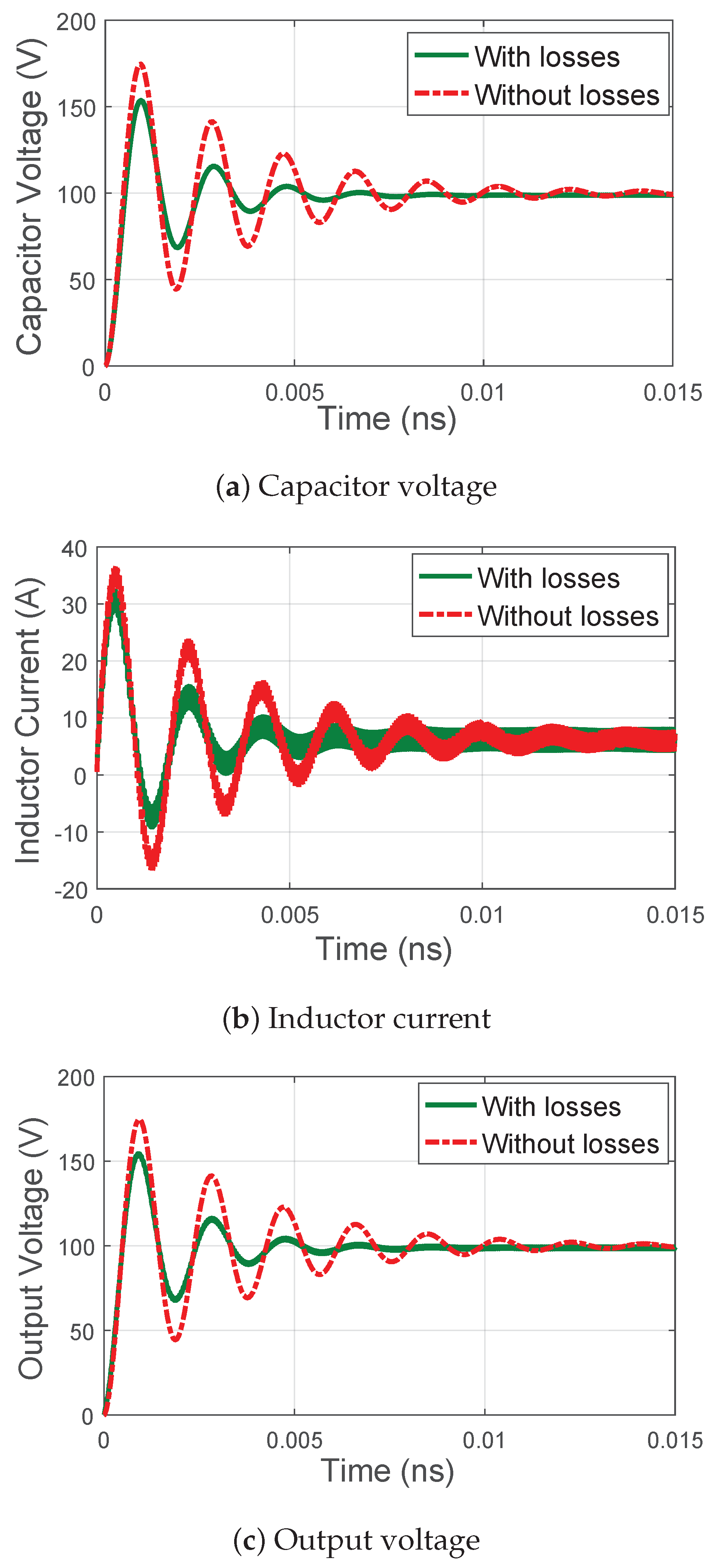
4. Results
As explained in
Section 2, this paper presents two different models of the full-bridge converter with and without losses intended to be implemented in FPGAs. As can be seen in
Figure 3, the model without losses produces noticeably different results, especially during the transient. The error of the model without losses is calculated in
Table 3, which is categorized into two different parts (transient and steady-state error). The steady-state zone is the interval in which the state variable of the model without losses is in the
band of the final value. It is obvious that the error of the model without losses cannot be neglected especially in the case of transient error. Thus, it is necessary to include different losses to the model as in
Figure 1b to have a more accurate model.
Once the importance of losses in the model is clear, the next question is which is the most appropriate numeric representation system. A thorough comparison is done between the reference model (real model) with losses and three other models with and without losses: floating-point 32-bits, non-optimized fixed-point, and optimized fixed-point. The accuracy of the reference model is previously confirmed by comparing its outputs with the same model in MATLAB/Simulink and the theoretical equations. The differences between the reference model and the MATLAB/Simulink model are shown in
Table 4. All the errors shown in this paper are MAE (Mean Absolute Error). The values in this table show that the results of the VHDL reference model match the simulation results in MATLAB.
The theoretical value of the output voltage without considering losses and with losses is calculated as Equations (
8) and (
9), respectively. The ripple and the mean value of the state variables based on the real model (reference model) are shown in
Table 5, which are compatible with the theory results in
Table 6 that shows the physical parameters of the implemented full-bridge converter. In all tests, the input voltage is a fixed 200 V dc voltage source and the switching frequency (
) is set at 20 kHz, while the duty cycle is 0.75. As can be seen, a resistive load has been chosen for the output load and the switching period (
) of the full-bridge model is 50
s.
In the following, all comparisons are done based on the reference model, which uses floating-point of double precision. This is to ensure that the only error sources are the numerical representation or the simulation time step, as all the other aspects are equal in the reference model and the rest of the compared models.
The proposed models were tested in open loop, without using any closed-loop regulators. This is important to compare the accuracy of the different models since a closed-loop regulation would lead to very similar results, masking small model inaccuracies [
5]. The control signals of the model were implemented with a simple DPWM (Digital Pulse Width Modulator). These inputs to the model, which define the switches states, are used for choosing the appropriate equations, as shown in Equation (
4). It is notable that, although in this example PWM signals are used for the control, the model actually reads the instantaneous values of the switches control signals, which are the inputs of the model, so any modulation can be used, without requiring constant frequency or any other limitation. The evaluation of the proposed systems is done by instantiating the different models, monitoring capacitor voltage, inductor current, and output voltage, and comparing those values with the ones of the reference model. As mentioned above, the reference model in VHDL is based on variables of real type and a simulation step of 1 ns.
Four different tests were done to show the numerical errors related to the different numerical formats. The first test focused on the error of different numerical formats with a simulation step of 1 ns. It is obvious that it cannot be reached in RT but it can be very useful to show the resolution problem in different approaches. The second, third, and fourth tests were carried out with simulation steps of 16, 20, and 24 ns, respectively. These simulation steps were chosen because they correspond to the limits of RT emulation when using optimized fixed-point, non-optimized fixed-point, and floating-point, respectively, as shown below.
Figure 4 shows the relation between the transient and the steady-state error of the capacitor voltage versus the clock period. As can be seen, the numerical error is nearly linear if the clock period is equal or greater than 16 ns. This situation can be seen in
Figure 4, where the accuracy of the models should be proportional to the simulation step, which means that the error of the model with a lower clock period should be smaller. This is the expected result because, as the simulation step is reduced, Equations (
5) and (
6) are more accurate. It is obvious that there is an anomaly in some of the models for a simulation step of 1 ns, but it is due to resolution issues in the numerical format.
The error of different numerical formats is very small but it can be analyzed in
Table 7,
Table 8 and
Table 9 regarding different integration steps. As can be seen in
Table 7, which has the same information as
Figure 4, the error is very similar between the different models when they use the same simulation step (
) if it is 16 ns or higher. This is because for those simulation steps the numerical resolution of all the models is high enough. However, when using
, the different models have quite different errors. That is caused by the insufficient resolution of some of the models, especially 32-bit floating-point and optimized fixed-point. The reason is that the increments in Equations (
5) and (
6), which are proportional to
, become so small that numerical issues appear. However, a simulation step of 1 ns is not achievable for RT emulation. This is just to show that numerical resolution issues may appear for high switching frequency converters (small simulation steps) depending on the application, and that the simulation step cannot be decreased indefinitely without also increasing the number of bits.
The other main conclusion of
Table 7,
Table 8 and
Table 9 is that, when numerical issues are not present, the error is mainly proportional to the simulation step. Thus, the design rule is to decrease the simulation step as much as the model allows. The minimum simulation step that can be reached in RT greatly depends on the complexity of the model, which determines the minimum achievable clock period for RT execution of each model.
Table 10 shows the synthesis results of the emulation systems after implementation in an xc7a35ticsg324-1L FPGA, which is a low-cost FPGA. The table presents the results in area and speed with and without losses. Three different synthesis results are provided including floating-point model, nOFPM, and OFPM. Furthermore, the three models were synthesized enabling and disabling the use of DSP blocks, to show the impact of these blocks on the rest of the necessary area (especially Look Up Tables (LUTs)) and necessary clock period. All previous models were hand-coded for optimum synthesis results. Besides, an automatic-translated model from MATLAB code to HDL using
Fixed-Point Designer/HDL Coder by MATLAB is shown in this table and is discussed below.
It can be seen that in all models with and without losses, the fixed point models require much fewer hardware resources than the float model, even 3 and 2.5 times fewer DSP blocks or LUTs and the minimum possible clock period is also up to 35% and 28% smaller in the models with and without losses, respectively. The main reason is that floating-point adders and multipliers are much more complex than fixed-point ones. It is notable that in these models, which are a direct translation of Equations (
5) to (
7), the FPGA clock period is equivalent to the simulation step. Therefore, fixed-point models can work in real-time using smaller simulation steps, which is the best way of minimizing model errors as seen before. This is also crucial for RT emulation of middle-high switching frequency converters.
Table 7,
Table 8 and
Table 9 highlight the error of each model when using their best achievable simulation step in each case: 16 ns for OFPM, 20 ns for nOFPM, and 24 ns for float 32.
Regarding both fixed-point models (nOFPM and OFPM), it can be seen that the OFPM implementation area is quite smaller than nOFPM (it needs fewer FPGA resources), and its maximum clock frequency is about 25% higher. It was expected, as OFPM uses fewer bits in general, and, furthermore, its widths are chosen for fitting exactly in one DSP block each one (multipliers bits).
In
Table 10, the synthesis results include versions without using the DSP blocks to clarify the impact of these blocks both in area and speed. In fact, most of the logic resources are dedicated to the multipliers, which are implemented in the DSP blocks. To have a fair comparison, it can be seen that the models with losses and without DSP blocks use 752 LUTs for OFPM, 1546 for nOFPM, and 2332 for floating-point. The same results are obtained for the models without losses as they use 472, 754, and 1182 LUTs for OFPM, nOFPM, and the float model, respectively. Removing DSP blocks is not a good approach because it can increase the minimum achievable clock frequency, as can be seen in
Table 10 for the OFPM. The minimum clock period (
), which is equal to the execution time needed by the FPGA to calculate the integration equations, is the most important parameter for comparing different notations because not only a small simulation step is necessary to emulate high-frequency converters but it also affects the error, as discussed above.
Table 10 also includes results of the automatic translation from MATLAB to HDL code using fixed-point. To have a fair comparison, this translation uses the same data widths of OFPM. Its synthesis results are clearly worse than the hand-coded OFPM with area sometimes approaching floating-point results and with time results even worse than hand-coded floating-point. Therefore, for optimum synthesis results, hand-coding is highly recommended.
The bar chart in
Figure 5 illustrates the numbers in
Table 10 to highlight the area and clock period differences between all models. As a conclusion, area results of the three models are quite different, which has a direct impact in the final price of the HIL systems. The number of LUTs when not using DSP blocks is about three times more in floating-point than in OFPM, and a similar or even higher proportion in the number of DSP blocks when they are enabled. It can also be seen that the minimum achievable clock period reduces if the OFPM is used, but in less proportion than area. Taking into account that fixed-point requires more design effort than floating-point, time results may not compensate the extra design effort depending on the application, but, when area is the main concern, fixed-point is highly recommended.


