1. Introduction
The fifth-generation (5G) millimeter-wave (mm-Wave) frequency range, also referred to as the frequency range 2 (FR2), includes the band between 24.25 and 52.6 GHz. For the 5G mm-Wave wireless applications, beamforming antenna system is essentially needed to cope with high free-space path loss, severe multi-path fading, and possible interference management for improving signal-to-noise ratio [
1,
2]. Two approaches are possible for the beamforming system realization. The first approach is phased-array beamforming system [
2]. It can provide continuously any-directional beam-steering capability, but requires sophisticated beamforming circuitry comprising precise phase shifters, variable gain blocks, and switches, thus it inevitably elevates the system implementation cost and complexity. On the other hand, switched beamforming antenna system can provide discontinuous discrete-directional beam-steering capability, but with much less hardware complexity and easier producibility. Thus, the switched beamforming antenna system is more preferred when precise and continuous beam steering function is not necessarily required, whereas implementation cost and producibility are of more importance. Passive beamforming matrices such as Blass matrix [
3], Nolen matrix [
4], and Butler matrix [
5,
6,
7,
8,
9,
10,
11,
12,
13,
14] are generally adopted for the switched beamforming antenna system. Among them, the Butler matrix is more widely used due to its wideband characteristic and simple structure.
When realizing a Butler matrix based switched beamforming antenna system, the Butler matrix usually occupies a much larger area than the antenna array elements. Thus, minimizing the Butler matrix size is more critical for the overall form factor minimization. Many previous works have been reported focusing on the miniaturization of the Butler matrix. The previous techniques can be categorized into a single-layer substrate based design [
5,
6,
7] and a multi-layer substrate based design [
8,
9,
10,
11,
12,
13,
14]. For the single-layer substrate designs, several techniques, such as a higher characteristic impedance transmission line based design [
5], a directional coupler employing lumped components [
6], and an artificial transmission line employing quasi-lumped elements and discontinuities structure [
7], were effective for the miniaturization. Nevertheless, since the Butler matrix and the antenna elements were put on the same plane, the spurious radiation leaking from the Butler matrix toward the antenna was a serious issue because it adversely affected the total radiation pattern.
The multi-layer substrate design approach can alleviate the spurious radiation issue more effectively because the Butler matrix and the antenna elements are placed in different layers. In addition, such previous multi-layer designs have employed further miniaturization techniques, such as the suspended stripline [
8], dual transmission line structure in a multi-layer structure [
9], forward-wave directional coupler [
10], modularized multi-folded structure [
11], slot-directional hybrid coupler [
12], and dual-layer substrate integrated waveguide (SIW) based crossover elimination structure [
13,
14]. Yet, it should be noted that those miniaturization techniques inevitably lead to higher implementation cost and less producibility. It is also interesting to note, that those previous works [
8,
9,
10,
11,
12,
13,
14] have utilized only the same-property homogenous substrates for the multiple layers.
In this work, we propose to adopt a two-layer hybrid stackup substrate for realizing a 28-GHz band Butler matrix based switched beamforming antenna system. The hybrid two-layer stackup substrate is composed of two dissimilar layers with each layer having optimal electrical properties for the Butler matrix and the antenna elements. Such hybrid stackup substrate based design approach was also found to be effective for performance and reliability improvement in the high-frequency serial-link applications [
15,
16]. This work is carried out to achieve the overall size miniaturization and the spurious radiation reduction in a Butler matrix based switched beamforming antenna system for 28-GHz mm-Wave 5G radio applications.
2. Design of Switched Beamforming Antenna System
The switched beamforming antenna system comprises a 4 × 4 Butler matrix and 4-element array antenna.
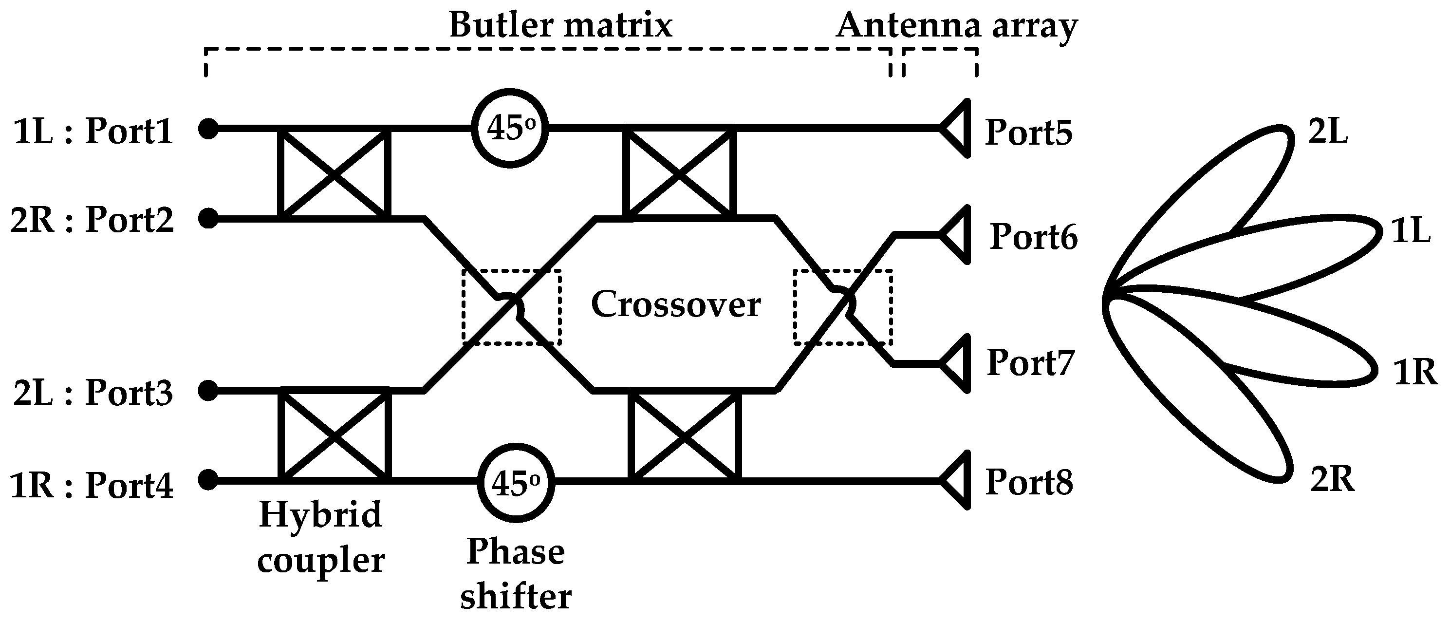
Figure 1 depicts the block diagram of the proposed antenna system. The 4 × 4 Butler matrix has four input and four output ports, and is composed of four 3-dB hybrid couplers, two cross-over structures, two 45° phase shifters. Depending on which input port among Port 1, 2, 3, and 4 is fed by input signal, the signal phases at the output ports (Port 5, 6, 7, and 8) are to show constant phase offsets of −135°, −45°, +45°, and +135° with respect to the adjacent output ports, respectively. As a result, the radiated beam is steered to the four discrete directions of −45°, −15°, 15°, and 45°, as illustrated in
Figure 1. The four steered beams are denoted as 1L, 2R, 2L, 1R with respect to the excited input port 1, 2, 3, and 4, respectively.
For the mm-Wave 5G applications, the microstrip patch-type antenna is widely used because of the simple structure, easy fabrication, and small size. The back lobe level is also reduced due to the back-side ground plane. Signal feeding structure from the Butler matrix to the patch elements should be carefully designed. Since the Butler matrix and the patch elements are placed in different layers in this work, probe feeding and aperture coupled feeding methods are possible. The aperture coupled feeding method as adopted in [
14,
17] is known to be more wideband than the probe feeding. However, it usually requires stricter alignment, otherwise the sidelobe level and impedance matching characteristics can be significantly affected especially in this mm-Wave high frequency region. In contrast, the probe feeding through a coaxial-structure through-hole-via does not need such strict alignment and thus more tolerant to the fabrication inaccuracy, and also has advantages of lower sidelobe and back-lobe levels. Thus, in this work, we employ the probe feeding through direct through- hole-via.
We have first carried out the block level designs for the 1 × 4 patch antenna array and 4 × 4 Butler matrix and optimized their performances independently. However, even though the block-level designs are well carried out, in this 28-GHz mm-Wave band, the overall system performances are very likely to be affected and degraded by interfacing and interconnecting the Butler matrix and antenna elements. From this point of view, some of the previous works were rather incomplete because they only presented Butler matrix miniaturization designs without realizing full integration with antenna array [
8,
9,
10,
11], or only connectorized interconnection [
12]. In this work, we have carefully carried out intensive co-optimization of the total system including the Butler matrix, antenna elements, and the interfacing structures in between.
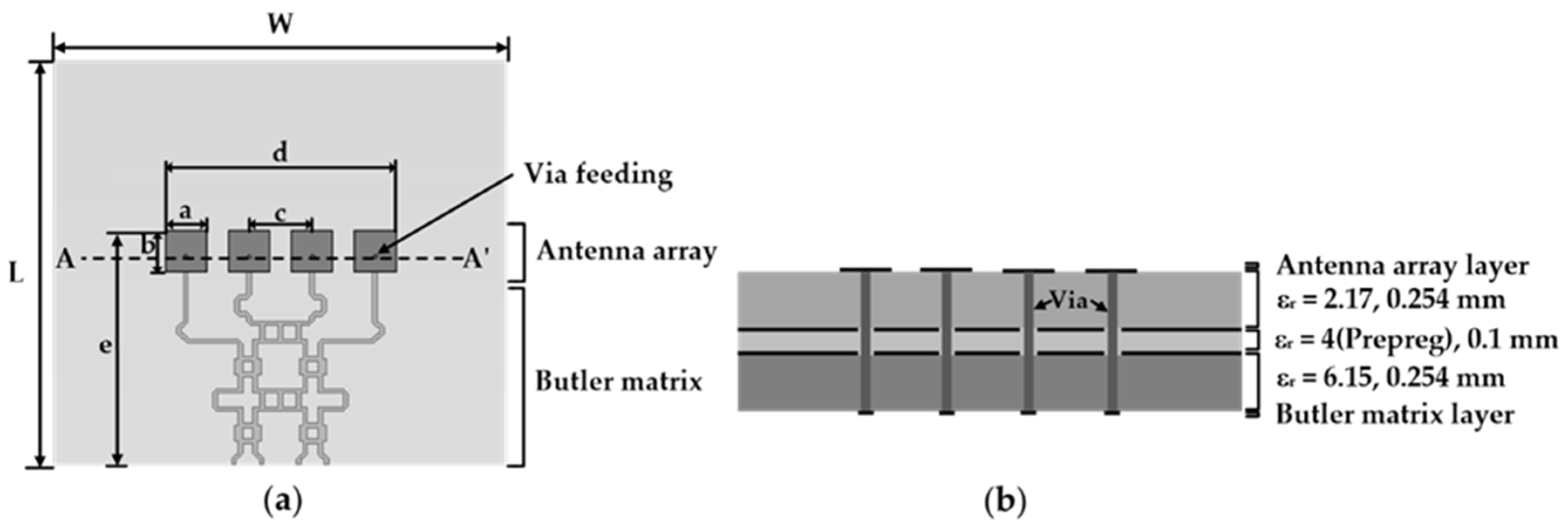
Figure 2 shows the proposed beamforming antenna system structure. The key dimensional parameters of the structure are given in
Table 1.
Figure 2a shows the layout top view, and
Figure 2b shows the cross-sectional view of A-A’ in
Figure 2a. The 1 × 4 patch antenna elements and 4 × 4 Butler matrix are placed on opposite outer sides of the two-layer substrate, and connected by through-hole via as illustrated in
Figure 2b. The two inner planes of the two-layer substrate are used as ground planes. The two layers are made of polytetrafluoroethylene (PTFE) material, but having different properties. The upper antenna layer has a dielectric constant ε
r = 2.17, tanδ = 0.0009, and thickness h = 0.254 mm, and the lower Butler matrix layer has a relatively higher dielectric constant ε
r = 6.15, and tanδ = 0.0028, and h = 0.254 mm. The two layers are attached by prepreg that has a dielectric constant ε
r = 4, and thickness h = 0.1 mm. The metallization thickness is 35 μm. The via diameter is 0.3 mm, and the anti-pad diameter is 0.5 mm. Thus, the spacing between the though-hole- via and adjacent ground plane is 0.1 mm. All the dimensions are the minimum allowed by the drilling process. We have verified through electromagnetic simulations that this via holes do not significantly alter the antenna radiation characteristics.
The single antenna element has a dimension of 3.3 × 3.3 mm
2, which correspond to 0.3λ where λ is the free-space wavelength of the operation frequency. The inter-element pitch is 5 mm. The patch dimension, inter-element spacing, and via position are carefully optimized for impedance matching and antenna gain. Since the antenna dimensions are governed by the substrate dielectric constant ε
r, the lower ε
r (= 2.17) layer is used as the antenna substrate because it is advantageous for higher radiation efficiency, reduced inter-element coupling, and higher fabrication accuracy, as a result, leading to much better and reliable radiation pattern with higher gain and lower sidelobe level. On the other hand, the Butler matrix is implemented in the higher ε
r layer because the Butler matrix size reduction dominates the overall size reduction. We have found that by simply using this higher ε
r (= 6.15) layer for the Butler matrix, the overall size reduction is significant even without adopting the previous sophisticated techniques reported in [
8,
9,
10,
11,
12,
13,
14]. Also, the proposed two-layer substrate design can effectively suppress the spurious parasitic radiation leaking from the Butler matrix side toward the antenna side, resulting in the overall radiation pattern improvement.
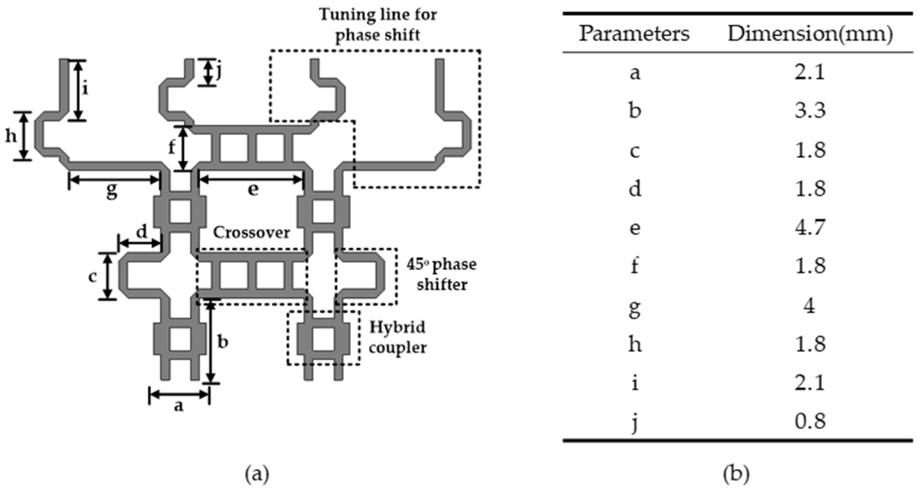
Figure 3 shows the details of the Butler matrix layout and its key dimensional parameters. It consists of four 3-dB hybrid couplers, two 45° phase shifters, two cross-over structures, and final tuning feed lines for additional fine adjustment of phase. The final tuning feed lines is included to cover about a 10° variations at the final output ports. All elements are designed in 50-ohm microstrip line type. In order to estimate the size reduction effect by using the higher ε
r (= 6.15) layer compared to using the lower ε
r layer, a similar previous work in [
18], which described a 28-GHz 4-directional switched beamforming antenna system in a ε
r = 2.2 substrate, is compared. Compared to [
18], we have found that 50 Ω microstrip line width is reduced by 54%, and the 45° phase-shift line length is reduced by 37%. Moreover, the Butler matrix’s total dimension of this work is 13 × 19 mm
2, whereas its dimension in [
18] is 37 × 45 mm
2. Thus, the overall size is reduced by 85%. Meanwhile, as shown in
Figure 2a, the total dimension including the antenna and Butler matrix is 18.3 × 22.5 mm
2, which corresponds to 1.7λ × 2.1λ.
The hybrid two layers have different thermal properties as well as different electrical properties. Thus, the thermal issue during fabrication process steps needs to be carefully taken into account for reliable mechanical characteristics. Typical fabrication process of the two-layer printed circuit board (PCB) is as follows. First, inner plane of each layer is independently fabricated through patterning, etching, and drilling processes. Then, a prepreg sheet is placed in the middle of the two layers. They are piled up according to the wanted construction, and bonded together by using heated press plates with high pressure. Finally, through-hole vias for electrical connections between the two outer layers are formed by drilling. The last step is patterning and plating for the outer layers. Since the two layers have different coefficients of temperature expansion (CTE), registration and warpage issues are likely to occur during the lay-up and heated press steps [
19]. The two layers used in this work are anisotropic materials. The CTE’s for the antenna layer are 20 and 280 ppm/°C, for x-y and z directions, respectively, and the CTE’s for the Butler matrix layer are 9, 8, and 69 ppm/°C, for x, y, and z directions, respectively. Assuming the process steps impose very even distribution of heat and pressure, and the whole PCB size is 1 × 1 m
2, the maximum dimensional offset in x-y direction will become 12 μm during the heated process, which is only 12% considering the anti-pad clearance rule of 100 μm. Thus, we have found that this is not a critical issue for at least the given PCB size. However, this issue should become more critical if the fabricated PCB size is larger in mass production.
3. Results
The whole antenna system is simulated and optimized by using a commercial full-wave 3-dimensional electromagnetic field simulator. Several selected key dimensions and jig structure are tuned to achieve optimal antenna performances through intensive electromagnetic simulations. The antenna system is fabricated in the hybrid two-layer substrate, for which the lower ε
r and the higher ε
r substrates as depicted in
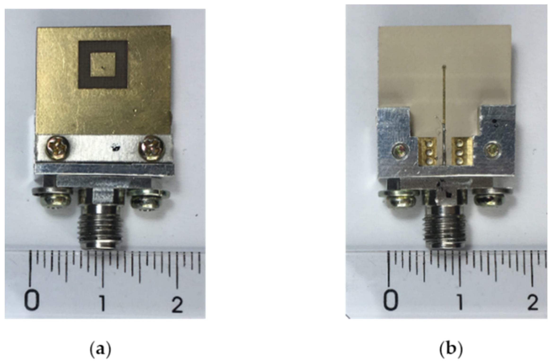
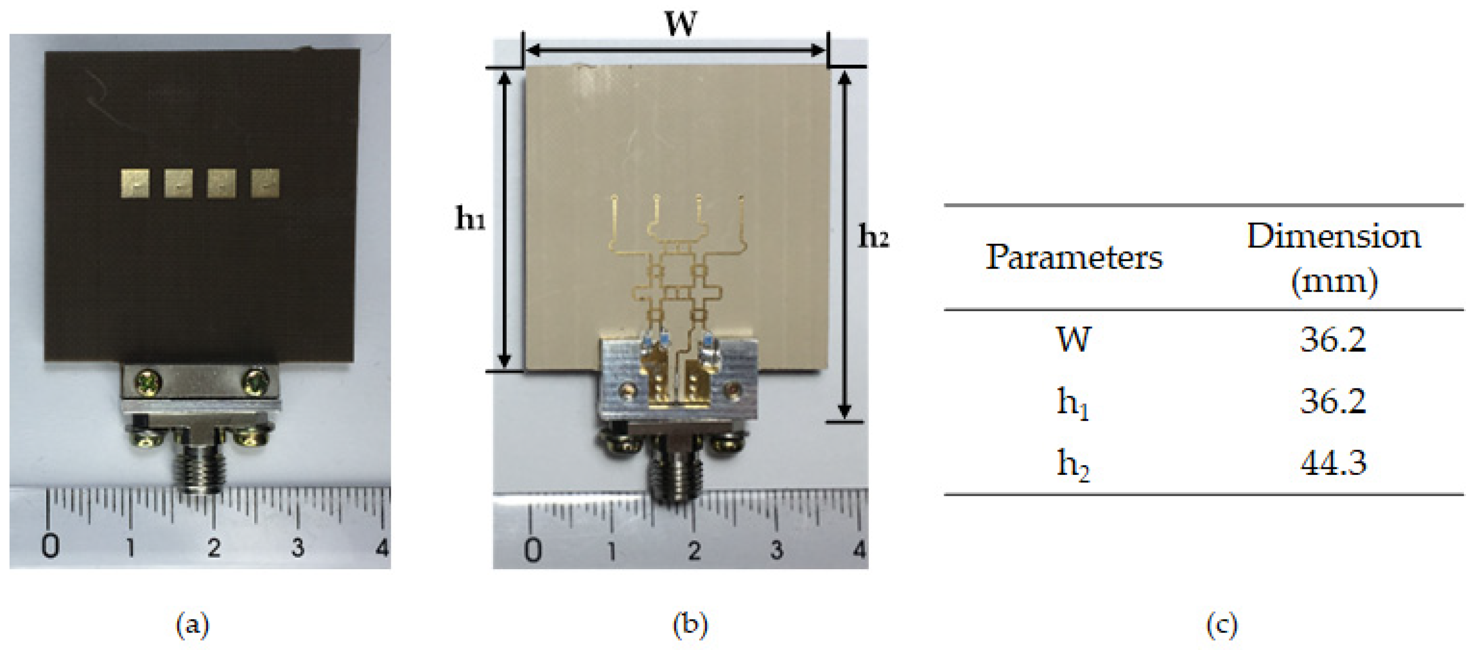
Figure 2b are chosen to be Taconic TLY-5A and RF-60A substrates, respectively. The microwave radiation characteristics are measured in an anechoic chamber. Careful calibrations were carried out to de-embed the cable and connector effects. For a test characterization purpose, a single element patch antenna is first fabricated in the proposed two-layer substrate.
Figure 4 shows a photograph of the fabricated antenna. The low dielectric constant increases the radiated power and efficiency.
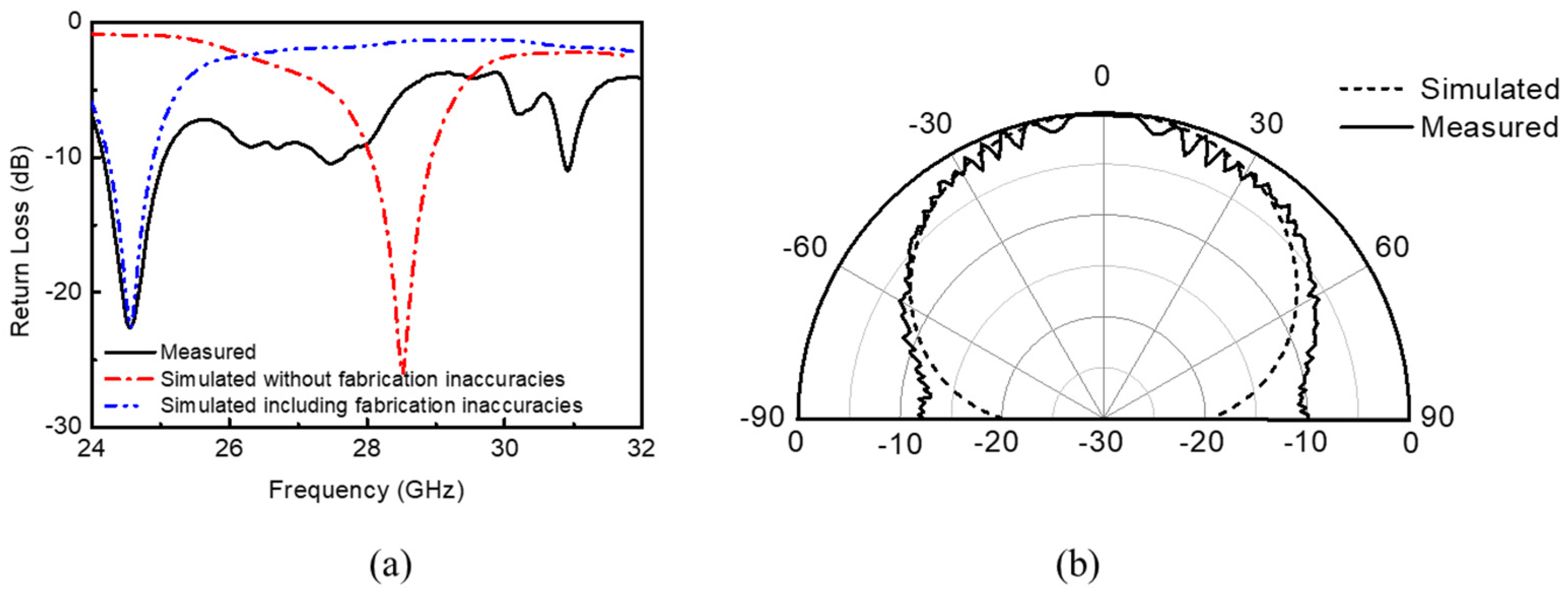
The simulated and measured results of the return loss and radiation pattern are plotted in
Figure 5. According to the simulation without considering fabrication inaccuracies and non-idealities, the impedance band with return loss < −10 dB was found to be 28.0–28.9 GHz. However, measured return loss shows that the impedance matching band is shifted down to 24.2–25.0 GHz, and at the same time 27.3–27.6 GHz band also appears as a matched band. We found that such discrepancy be attributed to the fabrication inaccuracies and non-idealities. For further investigation of the effects, intensive simulations are performed again with several possible fabrication inaccuracies assumed. Three fabrication inaccuracies assumed here are too much soldering on the connector pin, which can widen the feed line, slightly wider patterning during etching process, which can increase the patch dimension, and slight misalignment of drilling position, which can move the probe feeding point. When such inaccuracy parameters are changed by about 10–20%, as can be seen in
Figure 5a, the simulation result shows the excellent agreement with the measured result. This observation indicates that the fabrication inaccuracies and non-idealities must be minimized and avoided as much as possible in this mm-Wave frequency band. Meanwhile, as shown in
Figure 5b, the simulated and measured radiation patterns are well matched. The peak antenna gain is 7.4 dBi, and the front-to-back ratio is 25 dB.
The Butler matrix characteristics are evaluated using the same electromagnetic simulator.
Table 2 shows the simulation results of the relative phases and insertion losses at all ports. The ideal insertion loss of this Butler matrix must be 6 dB since it contains two 3-dB hybrid couplers. In simulation, the insertion loss is found to be 5.3–10.0 dB with an average of 8.1 dB. The relative output phases in ideal and simulated conditions are also given in
Table 2. The maximum error of the simulated phase with respect to the ideal phase is 16° for the signal paths of Port 1-to-Port 5 and Port 3-to-Port 8. The overall phase error in root-mean-squared value is calculated to be 7.4°. Applying the simulated phase and amplitude results of the Butler matrix to the antenna array input ports, we have found that, compared to the ideal excitation conditions, the gains are degraded by 2 and 2.8 dB and beam steering angles are tilted by −2° and +2°, for 1L/1R and 2L/2R beams, respectively.
The fabricated 4-directional switched beamforming antenna system is shown in
Figure 6. The antenna array is located at the center of the structure in order to minimize radiation disturbances that may be caused by asymmetric backside ground plane. Also, note that the ground pattern surrounding each antenna element at the front side as shown in the single patch antenna in
Figure 4a, is not adopted in this array implementation for the sake of simplification and miniaturization. Nevertheless, we have verified that such surrounding ground plane does not make any noticeable effects on the overall antenna characteristics. For measurements, input signal is fed to one of the four input ports via a 2.92 mm coaxial end-launch connector while three unused input ports are terminated by 50 Ω resistors. The 50 Ω resistors are used as available from [
20] as a part number CH0603-50RJNT. They are mm-Wave SMD components with dimension of 1.52 × 0.75 mm
2 and guaranteed performance up to Ka-band. The PCB jig is designed as small as possible just enough to hold the connector, but not to adversely affect the original antenna radiation characteristics. The total dimension of the fabricated switched beamforming antenna system is 36.2 × 44.3 mm
2 or equivalently 3.4λ × 4.1λ including the jig, while it is 36.2 × 36.2 mm
2 or equivalently 3.4λ × 3.4λ excluding the jig.
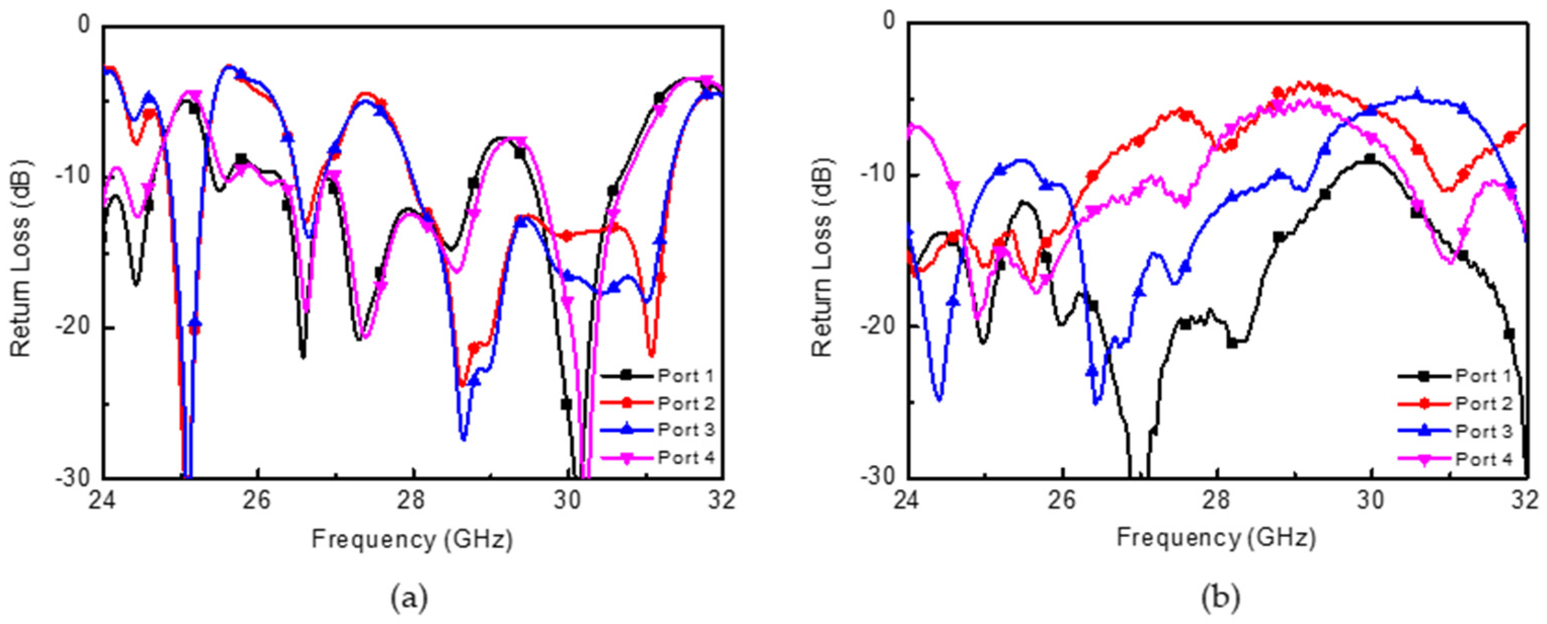
Figure 7 shows the simulated and measured return loss with respect to the four input ports. The simulated return loss is found to be less than −10 dB at 28 GHz, but the measured results show slight degradation, and is found to be about −8 dB at 28 GHz. Such degradation may be accounted for by fabrication inaccuracies and non-idealities such as swollen solder bumps, through-hole via misalignment, jig misalignment, and so on.
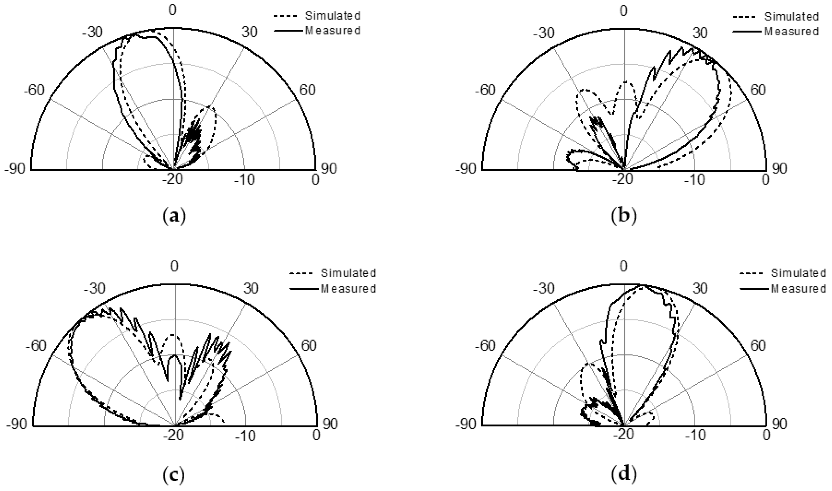
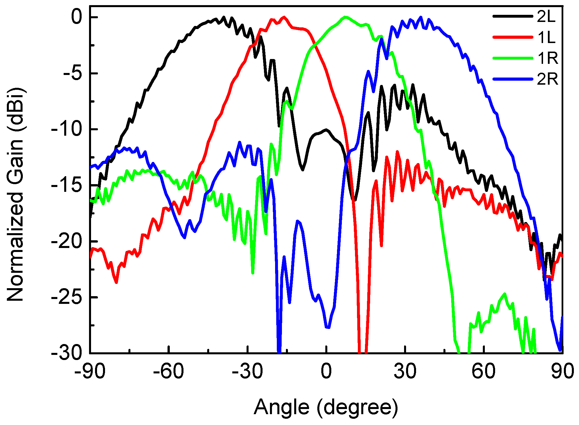
The radiation patterns are measured in an anechoic chamber by using the fabricated antenna as a receiving one.
Figure 8 illustrates the four-directional beam patterns by comparing the simulation and measurement results.
Figure 9 also shows the same measured radiation patterns in Cartesian format for the sake of more clarity. The peak gains are found to be +9.9, +8.8, +9.9, +8.5 dBi for 1L, 2L, 1R, and 2R directions. The beam steering angles are measured to be −16°, −39°, +7°, and +36° while the simulated beam steering angles are −13°, −43°, +13°, +43°, for 1L, 2L, 1R, and 2R, respectively. They are comparable to previously reported works in [
5,
13,
14,
17]. The simulated and measured sidelobe levels are observed as −9.5, −7.2, −9.8, −7.3 and −12, −6, −13.8, −11.7 dB for 1L, 2L, 1R, and 2R, respectively. Note that the typical sidelobe levels are comparable to the previous works, except for the worst sidelobe level of −6 dB for 2L beam. The overall agreement between the simulated and measured results are satisfactory.
Table 3 compares this work with previously reported Butler matrix based switched beamforming antenna systems operating at the mm-Wave frequency range. In literature, very limited number of works can be found to demonstrate full integration of Butler matrix and antenna array elements as well as switched beam steering performance. Only [
13] is found to operate in the same 5G mm-Wave frequency band as this work, whereas other works operate at a higher frequency band of 38 GHz [
14], 42 GHz [
17], and 60 GHz [
5]. The maximum beam steering angle and sidelobe level of this work are found to be comparable or slightly worse than others. Nonetheless, they are practically sufficient for 5G mm-Wave radio requirements.
Since this work focuses on the miniaturization technique, form factor comparison is of the most importance. For fair comparison of the form factor, we introduce a normalized size factor, which is calculated by dividing the given physical area by free-space wavelength squared and beam steering direction count. For example, the beam steering count is 5 for [
17], and 4 for [
5,
13,
14]. From this normalized size factor, it can be seen that this work demonstrates the smallest form factor. Also, note that this work is the only one that employs the hybrid stackup substrate for the form factor miniaturization, whereas all others are fabricated in a homogeneous stackup substrate with more sophisticated miniaturization techniques employed.


