Article

A 2.77 μW Ambient RF Energy Harvesting Using DTMOS Cross-Coupled Rectifier on 65 nm SOTB and Wide Bandwidth System Design

Graduate School of Informatics and Engineering, The University of Electro-Communications, Tokyo 182-8585, Japan
*
Author to whom correspondence should be addressed.
These authors contributed equally to this work.
Electronics 2019, 8(10), 1173; https://doi.org/10.3390/electronics8101173
Submission received: 15 September 2019 / Revised: 12 October 2019 / Accepted: 14 October 2019 / Published: 16 October 2019
(This article belongs to the Section Microelectronics)

Abstract

:
This paper proposes a structure of the μ W RF energy harvesting (RFEH) system that is used for scavenging RF power from an ambient environment. A cross-coupled rectifier (CCR) with floating sub-circuit structures was utilized in the application of dynamic threshold MOSFET (DTMOS) on Silicon on Thin Buried Oxide (SOTB) to obtain high drain conductance of the MOSFET. A wide bandwidth matching between antenna and rectifier was designed to receive energy from the orthogonal frequency division multiplexing (OFDM) RF signal with a bandwidth of 15 MHz at 950 MHz band. Realistic measurements with a 950 MHz LTE mobile phone signal from the ambient environment indicate that an average DC output power of 2.77 μ W is harvested with the proposed RFEH system at a level of −19.4 dBm input power. The proposed RFEH system exhibits the best performance when compared to that of other realistic RFEH systems and is a potential candidate for battery-less Internet of Things (IoT) applications.

1. Introduction

Recently, energy harvesting (EH) has attracted a considerable amount of attention because it is an essential solution to eliminate the need for a battery in Internet of Things (IoT) applications [1]. An EH system harvests energy from an ambient source and converts this energy into DC power that is supplied for a sensor node. Energy sources in the environment include multi-forms such as: solar energy, thermal energy, ambient RF energy, and piezoelectric energy [2]. In this context, an RFEH system demonstrates its importance owing to its continuous and well-known properties by harvesting an RF signal in the ambient environment.
A disadvantage of the RFEH is that the RF signal level in an environment is low. A power density of an RF signal in [2] was presented in a range of 0.2 nW/cm 2 –1 μ W/cm 2 . In [3], measurement results showed that the median power value of a digital TV signal was −38 dBm, and that of a mobile phone signal was −25 dBm. In [4,5,6,7,8], the RFEH systems were designed and tested in real ambient environments at an μ W level range.
In the RFEH system, a rectifier is used to convert an RF input signal to a DC output signal. The low input power of the RF signal leads to difficulties in the design of the rectifier circuit. In this case, the RF level is lower than the threshold voltage ( V t h ) of the rectified components, resulting in significant decreases in power conversion efficiency (PCE) of the system.
Several solutions were presented to increase the PCE of the system in the μ W input power range. For the rectifier, preferred techniques include V t h cancellation techniques, such as static V t h cancellation technique [9], differential-drive topology [10,11,12], and floating sub-circuit bias [13]. Some authors proposed solutions for harvesting an RF signal in the environment by gathering a multi-band ambient RF signal such as designing multi-band antennas, multi-band matching circuits, and multi-band RF-DC conversion circuits [5,14,15,16]. A co-design of antenna and rectifier was proposed and demonstrated outstanding results in terms of sensitivity and PCE [17,18].
Although several studies have focused on RFEH, the majority of the studies tested their full RFEH system performance with an RF signal from a dedicated source and not a realistic RF signal from an ambient environment [11,18,19]. Minor information on measurement results from a realistic ambient signal are reported in [5,6,7,17,20]. The results in the studies are limited to short time measurement.
The target of the present study involves designing an RFEH system that harvests the real RF signal from the environment. Based on the properties of the RF signal in the environment, including low level modulated LTE signals, the structure of the RFEH system was proposed. The dynamic threshold MOSFET (DTMOS) was proposed for application in a cross-coupled rectifier (CCR) with a floating sub-circuit to reach a high drain conductance rectifier. A wide bandwidth matching between antenna and rectifier is designed to ensure harvesting an entire bandwidth of the modulated RF signal. A dipole antenna matching with the rectifier was designed to complete the proposed RFEH system. With the proposed RFEH, measurements were performed in an indoor condition where a 4 LTE mobile phone signal was received, and the distance from a mobile phone base station to the measured position was 162 m. At −19.4 dBm input band power, the proposed RFEH system can generate 2.77 μ W average DC output power. The system shows stable performance through 24 h measurement, and 0.238 J was generated in a day. The results affirm the efficiency of the system and success in performing the target of design.
The paper is organized as follows: in Section 2, the spectrum of the ambient RF signal is presented. Then, the structure and design of the RFEH system to scavenging the ambient RF power is proposed in Section 3. We demonstrated the RFEH power harvested by the proposed RFEH systems in Section 4, followed by a conclusion in Section 5.

2. Ambient RF Power Structure

The ambient RF signals were measured in an office room at the University of Electro-communications, Tokyo, Japan. A signal analyzer Agilent CXA N900A and a dipole antenna CANDOX 44Sa21 were used to measure the spectrum of the RF signals in the environment. In measurement, a few specifications were set up as follows: resolution bandwidth was set at 100 kHz, and band power, which covers bandwidth (BW) of RF signals in the environment, corresponds to 15 MHz. The received power corresponds to the total band power that is set up as previous specifications. The received spectrum is shown in Figure 1.
As shown in the Figure 1, the RF signal at 952 MHz is the strongest, the power density at 100 kHz BW resolution is about −40 dBm, and the band power at 15 MHz BW is approximately at the −20 dBm level. The magnified spectrum of the 952 MHz signal is shown in Figure 1b. From the characteristics of the signal, it is concluded that the signal corresponds to an LTE downlink mobile phone signal with an orthogonal frequency division multiplexing (OFDM) modulation. Figure 2 shows the map of the measurement position. The mobile phone base station and antenna were located at the top of a building. The measurement position is in the center of the office room on the third floor. The measurement point and the base station are approximately 162 m apart.
From the measurement results, the target RF signal of the proposed RFEH system is the 952 MHz LTE mobile phone signal. The BW of the RF signal is approximately 15 MHz. Hence, BW of the RFEH system would be designed to be larger than 15 MHz for harvesting the RF signal from the ambient environment. Notably, such RF signals from 4G cell phone base stations are widespread in the ambient environment today where people are living in the world. Therefore, cell phone RF energy is one of the ideal energy sources for RFEH.

3. Structure of RFEH System

There are two main characteristics of the environmental RF signal which decide the configuration of the RFEH system, which are power level and modulation type. Studies to improve the power conversion efficiency (PCE) of rectifier in low input power range were proposed [10,17,20]. High Q circuit, which has high passive voltage gain, is an effective solution to boost PCE. The effect of modulated type of RF signal to the efficiency of the RFEH system is also analyzed [21,22,23].
Besides, the BW of the RF signal is an essential characteristic that affects the configuration of the RFEH system. The relationship between Q factor and BW of a resonator [24,25] is shown as in Equation (1)
Q = ω 0 E s P D o r Q = f 0 Δ f
where E s is energy stored in the resonator, P D is average power dissipated in the resonator, ω 0 is the resonant frequency in radians/second, f 0 is the resonant frequency in Hz, and Δ f is the BW.
From the equation, the Q factor is limited by the BW of the target RF signal. For example, to harvest the LTE mobile phone signal, which has 15 MHz BW, as mentioned in Section 2, the Q factor should be smaller than 63. However, the BW of the matching circuit needs to be wide enough to cover the BW of the RF signal to ensure that no RF power is lost.
In this study, to harvest the LTE signal, we proposed the structure of the RFEH system comprising a high drain conductance rectifier and a wide BW matching between antenna and rectifier. The Q factor of the proposed RFEH system is limited to ensure the BW of the LTE signal, resulting in the PCE of the proposed system harvesting a sine wave signal is smaller than other high Q harvesters. However, the PCE of the proposed system, when harvesting the LTE signal in the environment, is the highest in comparison to the other studies at the same input power level. The results prove the efficient structure of the proposed RFEH system.

3.1. DTMOS CCR with Floating Sub-Circuit

In the dynamic threshold voltage MOSFET (DTMOS) technique, the body of the MOSFET is tied to the gate. A very low voltage on the DTMOS technique to obtain a much higher current drain than regular MOSFET has been reported [26]. In the energy harvesting technique, DTMOS is applied to the rectifier circuit as a diode-connected rectifier [27], self V t h cancellation configuration [28], cross-coupled rectifier [29]. In our study, we propose the application of DTMOS to CCR with floating sub-circuits. Generally, the RF level in an environment ranges from −30 dBm to −10 dBm. At this level, we proved the amount of DC voltage level-up obtained from floating sub-circuit driving to DTMOS leads to an increase in drain current. The drain current of the proposed circuit is the highest when compared to the other configurations.
The proposed circuit was fabricated on 65 nm Silicon on Thin Buried Oxide (SOTB) CMOS technology [30]. In this technology, the threshold voltage of the MOSFET can be modulated by body bias, such that DTMOS performance is more effective. The body bias constant is defined by Equation (2)
α = Δ V t h Δ V B S
The body bias constant is almost 150 mV/1 V at SOTB [31]. This value is higher than that of a conventional Bulk CMOS. The effectiveness of DTMOS in terms of decreasing the threshold voltage of MOSFET when compared to the body-tide-to-source MOSFET (BTMOS) in the 65 nm SOTB technique was reported earlier [32]. The RF characteristics of SOTB 65 nm technology are validated in [33], and f m a x of PMOS and NMOS of SOTB devices are 20 GHz and 28 GHz, respectively. These parameters proved that the SOTB technology works effectively at 1 GHz frequency range.
The CCR with floating sub-circuits was first proposed in [13]. One stage of the rectifier circuit is shown in Figure 3. The circuit consists of three CCRs, namely the main CCR and two CCR sub-circuits. The sub-circuits include open loads to increase the DC voltage levels at points OP1 and OP2, resulting in the DC levels at FL11, 12, 21, 22 also increasing. These voltages are supplied to the gates of MOSFETs in the main CCR. Therefore, in comparison to a conventional CCR, the scheme supplies a higher DC level to the gates of the MOSFETs. In the main CCR, W/L of NMOSs and PMOSs are 2.4 μ m/60 nm, coupling capacitors, C c m are 1 pF each. Coupling capacitors in the CCR sub-circuit C c s are 0.5 pF each.
V G S N 1 = V R F 2 V R F 1 + Δ V D C
Considering the NMOS N1 in the main CCR, as shown in Figure 3, in forwarding bias region, the gate of N1 corresponds to FL12, and the source of N1 corresponds to M1. The difference in the levels of DC voltages between the points is denoted by Δ V D C , as indicated in Equation (3). The voltage Δ V D C represents the effectiveness of CCR with floating sub-circuits in comparison to a conventional CCR. Figure 4 shows the simulated dependence of Δ V D C on the input power in the CCR with floating sub-circuits. As shown in Figure 4, at the target input power range, the floating sub-circuit brings an amount of DC voltage to the gate-to-source voltage of MOSFET in the main CCR. At an input power of −20 dBm, the amount of Δ V D C becomes 63 mV.
Figure 5 shows the simulated results of IV characteristics in 4 configuration types: diode-connected BTMOS, diode-connected DTMOS, DTMOS in CCR, and DTMOS in CCR with floating sub-circuits. As shown in the figure, with the same diode-connected configuration, DTMOS brings higher drain current than BTMOS. When applying DTMOS to CCR and CCR with floating sub-circuits, the drain current of the latter configuration is higher than the former. It is concluded that the application of DTMOS on CCR with floating sub-circuits provides the highest drain current of the MOSFET, thereby increasing the efficiency of the rectifier in low input power range as compared to that of other configurations.
Figure 6 shows the simulated Q factor Q R E C T of the rectifier depending on the number of rectifier stages at 950 MHz and the level of input power ( P I N ) of −20 dBm. In the simulation, the effect of parasitic components of on-chip, off-chip pads, and bonding wires is accounted for.
From Equation (1), to guarantee the BW of the RF signal, which is 15 MHz at the center frequency of 950 MHz, the Q factor should be smaller than 63. Generally, a designed BW and a real BW are not identical. From Figure 6, the Q factor of a 3-stage rectifier is 43; hence, BW is 20 MHz. This BW is large enough to ensure discrepancy design between the designed BW and real BW. Therefore, the number of stages is chosen as 3.

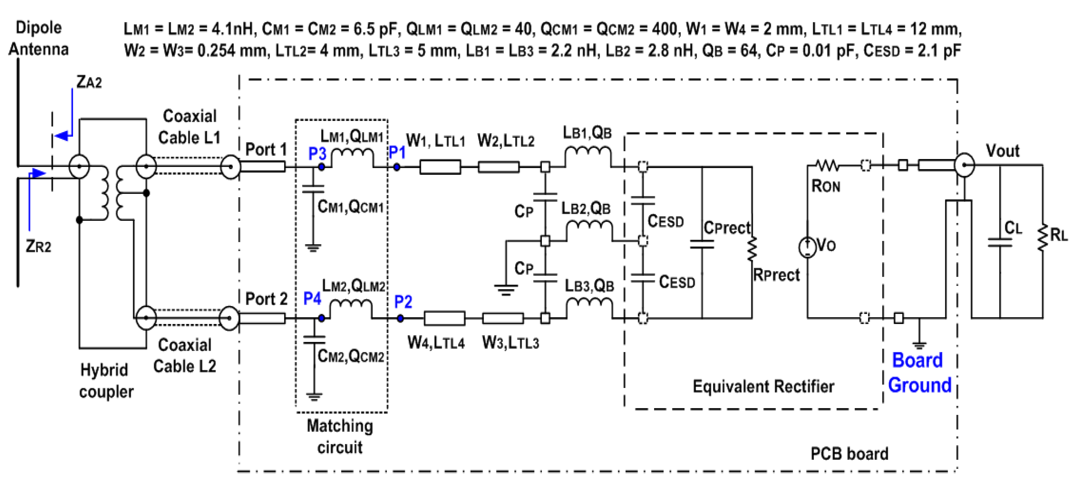
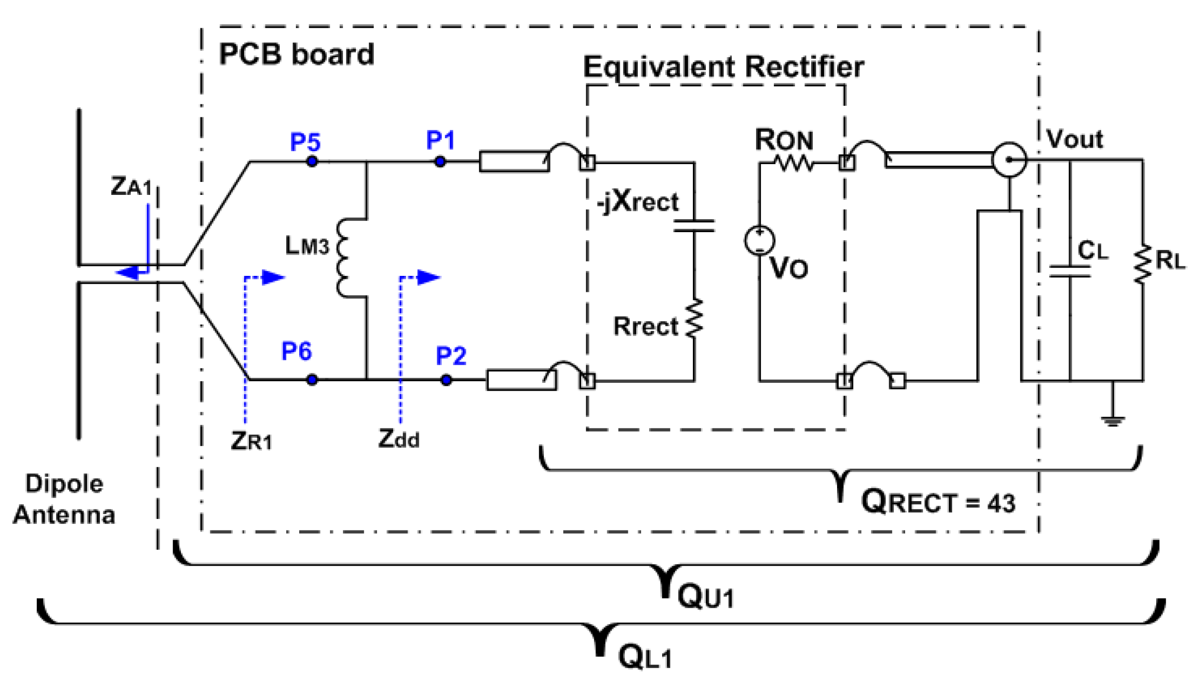
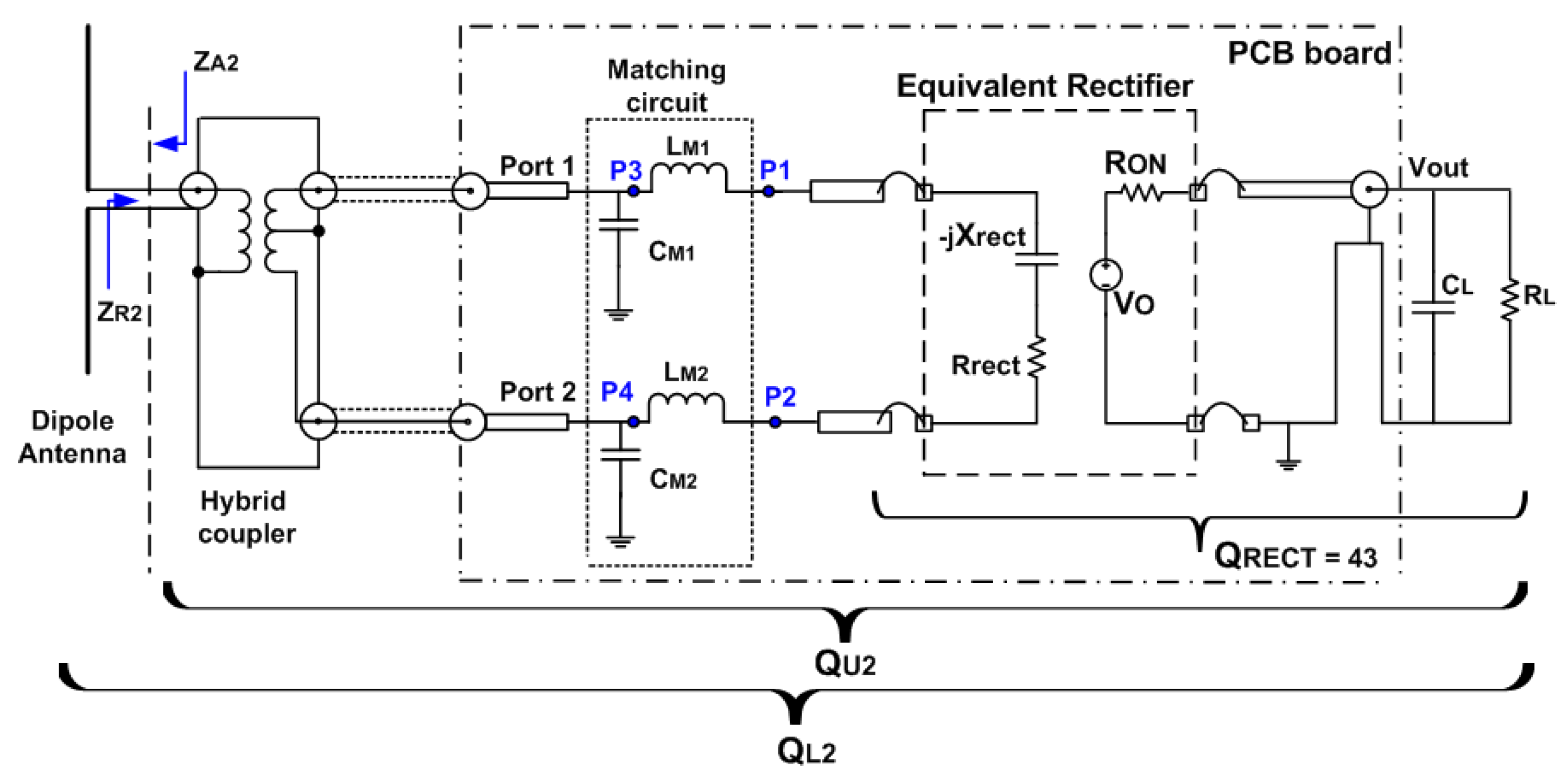
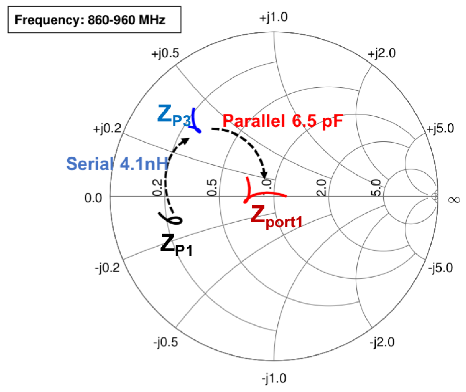
3.2. Matching Circuit and Antenna Structure

The rectifier chip is attached to a FR4 PCB board. Two configuration schemes of the RFEH system are designed and implemented, as shown in Figure 7. In the RFEH scheme 1, a dipole antenna is directly connected to the rectifier board. In the RFEH scheme 2, a hybrid coupler Krytar 4010124 is used to connect an antenna and the rectifier board. The RFEH scheme 1 is designed so that the system can harvest the RF energy from the ambient environment. The simple dipole antenna is utilized for the practical use of RFEH. The RFEH scheme 2 is mainly used to obtain experimental data using a signal generator and an RF energy source.
Figure 8 shows equivalent circuit of RFEH scheme 1. In the figure, Q U 1 is unloaded Q factor, and Q L 1 is loaded Q factor at feed-point of the antenna of scheme 1.
When system matched, Q L 1 is calculated by Equation (1). The relationships between Q R E C T , Q U 1 , and Q L 1 are shown in Equations (4) and (5):
1 Q U 1 = 1 Q R E C T + 1 Q e
Q U 1 = 2 Q L 1
where Q e is a Q factor of external components in the PCB, which consists of transmission lines, matching component L M 3 . To reduce loss, Q e should be maximized. In the proposed system, to increase Q e , the transmission line is short, which only 16 mm, and high Q matching components are chosen for the matching circuit. Besides, Q R E C T should dominate the Q factor Q U 1 and be moderate value to ensure the BW of the RF signal. When conditions are guaranteed, the BW of the RFEH system is wide enough to harvest the target RF signal.
The S parameter of the system is measured by a network analyzer ENA E5071C. In Figure 8, the impedances Z R 1 from point P5 to P6 and Z d d from point P1 to P2 correspond to differential-to-differential impedances. The impedance Z d d is 1-j*15.4 at 950 MHz. An inductor of 2.7 nH is added as the matching component. Figure 9a shows the measured impedances Z d d , Z R 1 and Z A 1 at the target frequency band from 940 MHz to 960 MHz. To match with a capacitive impedance Z R 1 , a 16-cm wired dipole antenna which length is equivalent to 0.51 wavelength of 950 MHz is designed.
Figure 9b shows S11 of the RFEH scheme 1. Bandwidth at −3 dB level is from 926 MHz to 988 MHz which is equivalent to 62 MHz BW. The center matched frequency is 959 MHz. Q L 1 and Q U 1 calculated from Equations (1) and (5) are 16 and 32, respectively.
In the RFEH scheme 2, the hybrid coupler is used to divide the received RF power from the antenna into two differential RF signals that are supplied to the rectifier with 180 0 phase difference. The effect of phase differences between the two paired RF inputs was validated [32]. With the hybrid coupler, the phase difference becomes exactly 180 0 ; hence, the output voltage is maximized.
Figure 10 presents equivalent circuit of the RFEH scheme 2. The detail circuit and parameters of components in the PCB board are shown in the Appendix A of the paper.
Matching circuits are attached at P1 and P2 points in the PCB board, as shown in Figure 10. Input impedance at the points P1 and P2 are 9-j*5 and 8.4-j*5. In the scheme, matching circuits are used to match P1 and P2 with 50 Ω ports, Port1 and Port2, respectively. L type matching circuit consisting of a 4.1 nH inductor and a 6.5 pF capacitor is designed as shown in Figure 11.
Figure 12 shows the simulated and measured reflection coefficients S11 at Port 1 and Port 2, respectively. Because the rectifier is a nonlinear circuit, so harmonic balance method (HBM) of advanced design system (ADS) software is used for simulation. At each frequency, input power is set up, then input voltage and current are simulated. From these parameters, an input impedance of the rectifier at specified input power and frequency is defined. The simulated S11 is calculated from the input impedance of the rectifier. Figure 12 indicates that the simulated and measured results are almost identical. The frequency band of the target RF signal corresponds to a range of 945–960 MHz, which is within the −10 dBm loss band.
Figure 13a shows a measured impedance of the RFEH scheme 2. The impedance at the feed point of scheme 2, which is denoted by Z R 2 in Figure 8, has an inductive property. A 14.3-cm wired dipole antenna whose length is equivalent to 0.45 wavelength at 950 MHz is designed to match with the rectifier. The Figure 13b shows S11 of the RFEH scheme 2. Bandwidth at −3 dB level is 41 MHz from 928 MHz to 969 MHz. A center frequency is 954 MHz. Q L 2 and Q U 2 calculated from Equations (1) and (5) are 23 and 46, respectively.

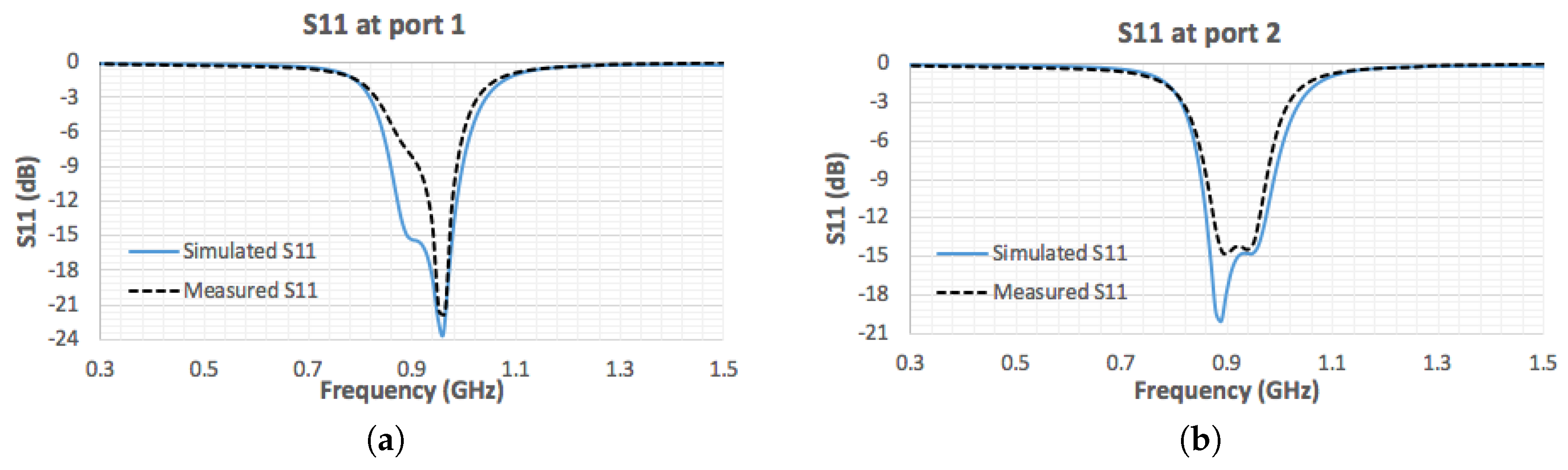
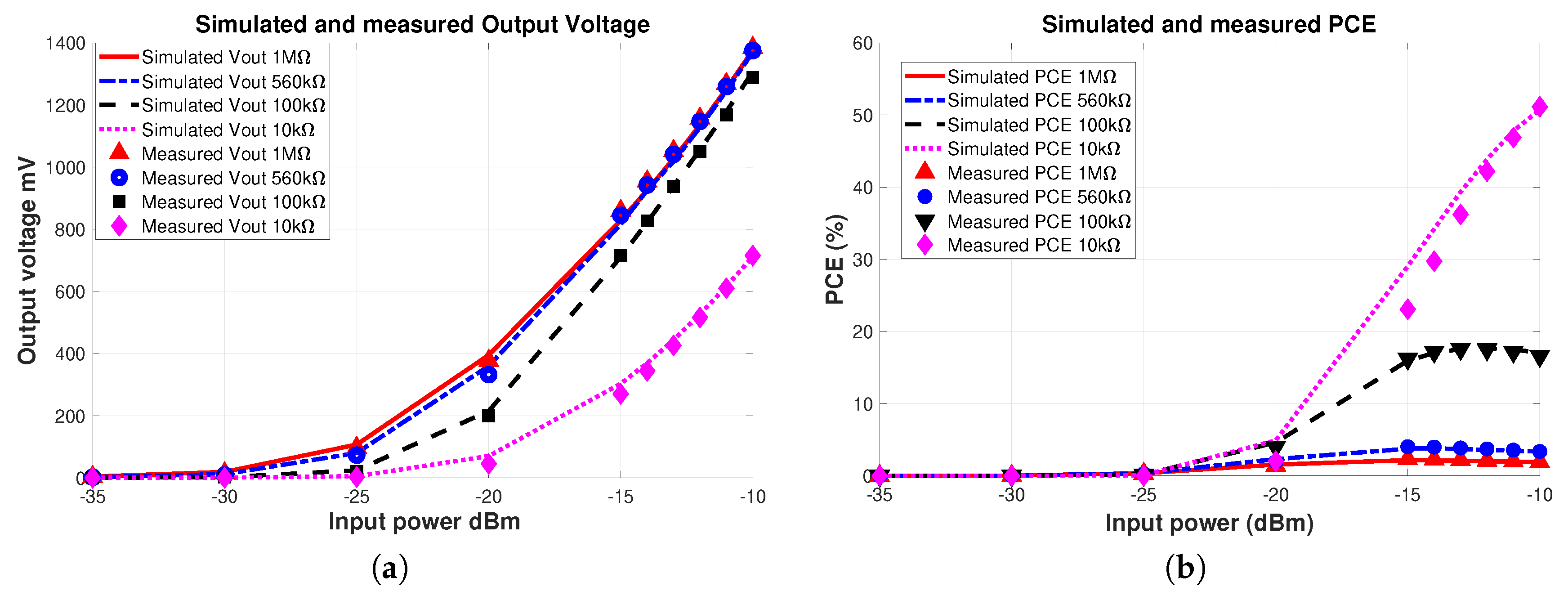
4. Measurement Results

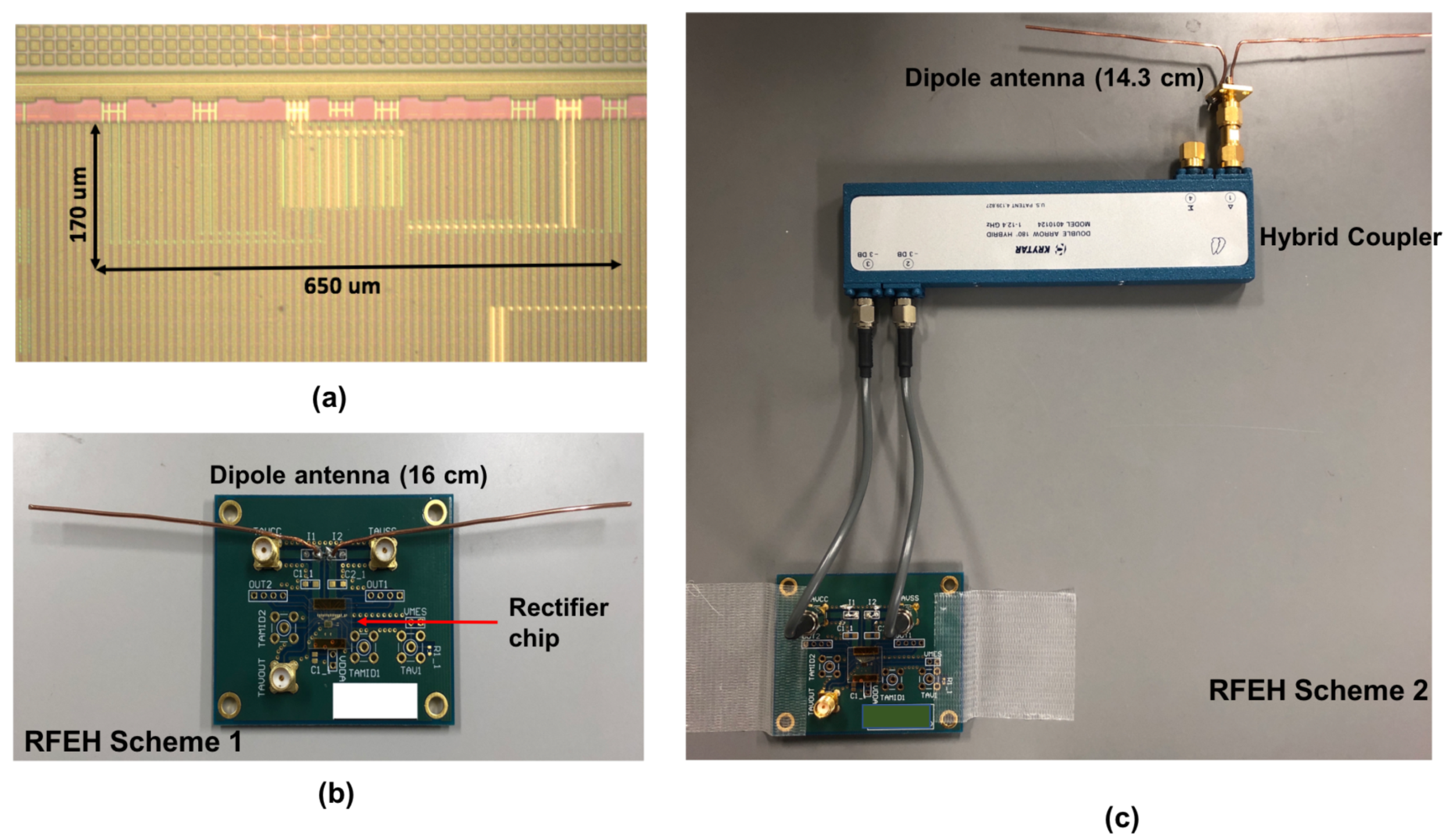
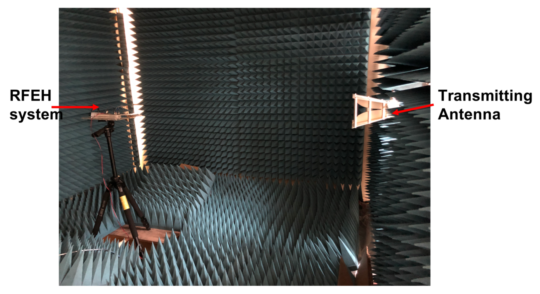
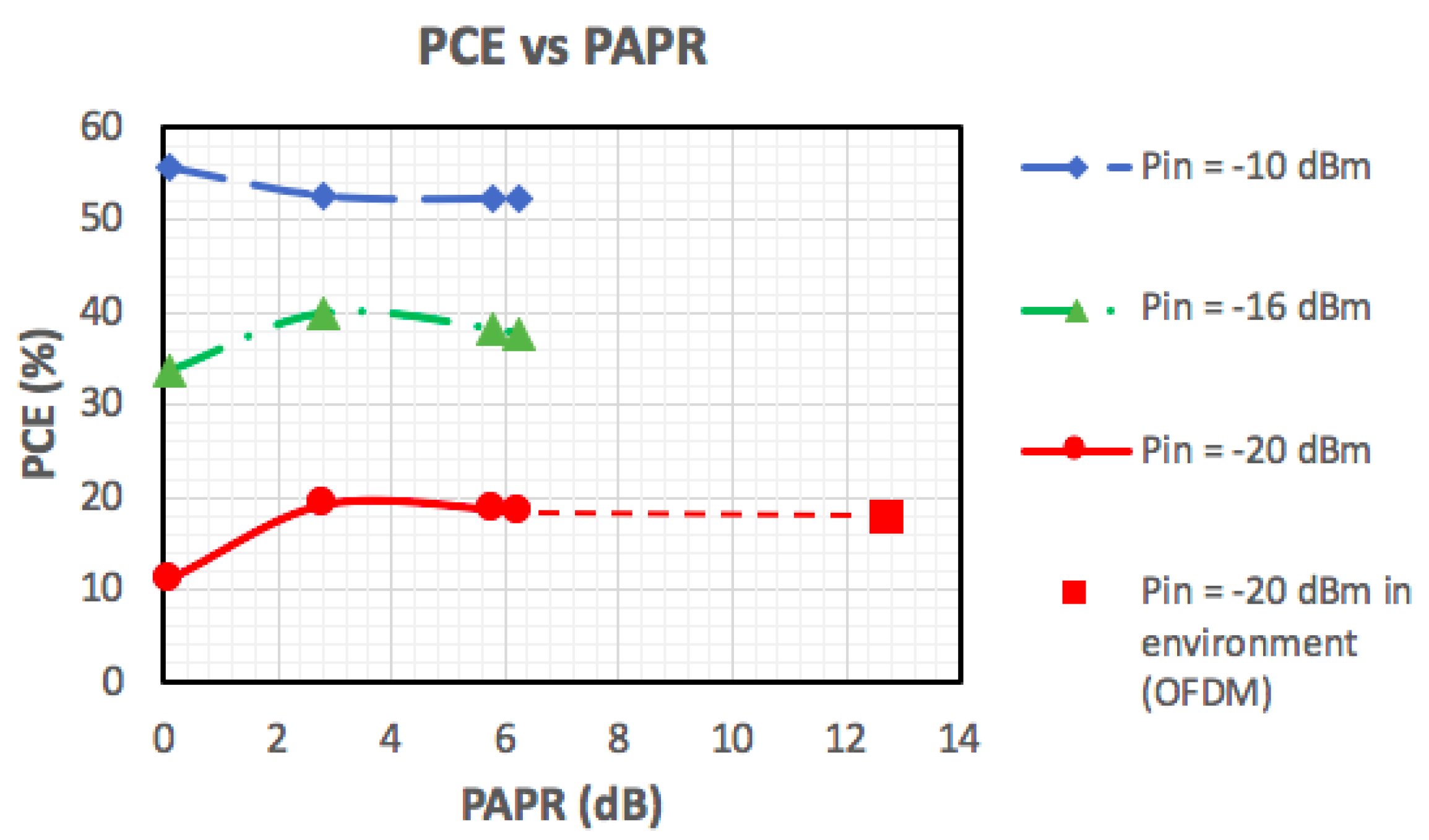
4.1. Measurement in Anechoic Chamber

In this measurement, the RFEH scheme 2 is used. We first evaluate the characteristics of the rectifier with a signal generator SMJ100A. The signal generator generates the RF signal as input to the hybrid coupler of scheme 2. The hybrid coupler then divides the RF signal into two differential signals and supplies the signals to the rectifier. Figure 14 shows simulated and measured results when the RF signal is a continuous sine wave (CW) signal at a frequency of 950 MHz. As shown in the Figure, the rectifier reaches a sensitivity of 1 V at an input power of −13 dBm at 560 k Ω . The highest power conversion efficiency (PCE) at a level of −10 dBm input power corresponds to 51% at a load of 10 k Ω .
The simulation results are obtained from the HBM in the ADS. The PCE is calculated by Equation (6):
P C E ( % ) = P D C o u t P R F i n 100 % = V o u t 2 R L P R F i n 100 % = V o u t 2 P R F i n R L 100 %
where P R F i n is RF input power, P D C o u t is DC output power. V o u t is output voltage at load R L .
The proposed RFEH system was measured in an anechoic chamber, as shown in Figure 15. The RF power at the measurement point is defined by measuring the received power using a reference dipole antenna, CANDOX 44Sa21.
Figure 16, Figure 17 and Figure 18 show the measurement results of the proposed RFEH in the chamber room. The rectifier circuit is designed to match with the antenna, thereby achieving higher results when measuring in an anechoic chamber as compared to those obtained with a signal generator. In Figure 16a, the output voltages of the proposed system at 10 M Ω load are presented. The sensitivity 1 V is obtained at a level of −17 dBm input power of modulated signals. Figure 16b shows the PCE of the proposed RFEH system when harvesting CW signals at different input powers and loads. From the Figure, the highest PCE of 57% is achieved at −10 dBm input power and 10 k Ω load.
Figure 17 shows the PCE of the proposed system at different input power levels when the RFEH system harvests the CW signal and modulated signals. The characteristic of the modulated signal is defined by a Peak-to-Average-Power ratio (PAPR). The PAPR was evaluated when a Complementary Cumulative Distribution Function (CCDF) of the signal is 0.001% [21]. In our measurement, PAPRs of CW, BPSK, 64 QAM, and 256 QAM signals are 0.1 dB, 2.82 dB, 6.23 dB, 5.76 dB, respectively.
At a level of −20 dB input power, the PCE of the RFEH system harvesting the modulated signal obtains 19%, while that of the system harvesting the CW signal is only 11%. At −10 dBm input power, the PCE of the system, when excited by the CW signal, is the highest, which is 57%. The results indicated that modulated signals boost the efficiency of the proposed system at the low input power range.
Figure 18 shows the relationship between PCE and PAPR of the modulated signals. In the chamber room, when harvesting modulated signals at a level of −20 dBm power, the PCE of the proposed system is 19%. At the same level, the efficiency of the system reaches 18% when harvests OFDM signal in the environment. The results prove the efficient performance of the proposed system in a real ambient environment and essentially an agreement with the results obtained from measurements done in the anechoic chamber room.

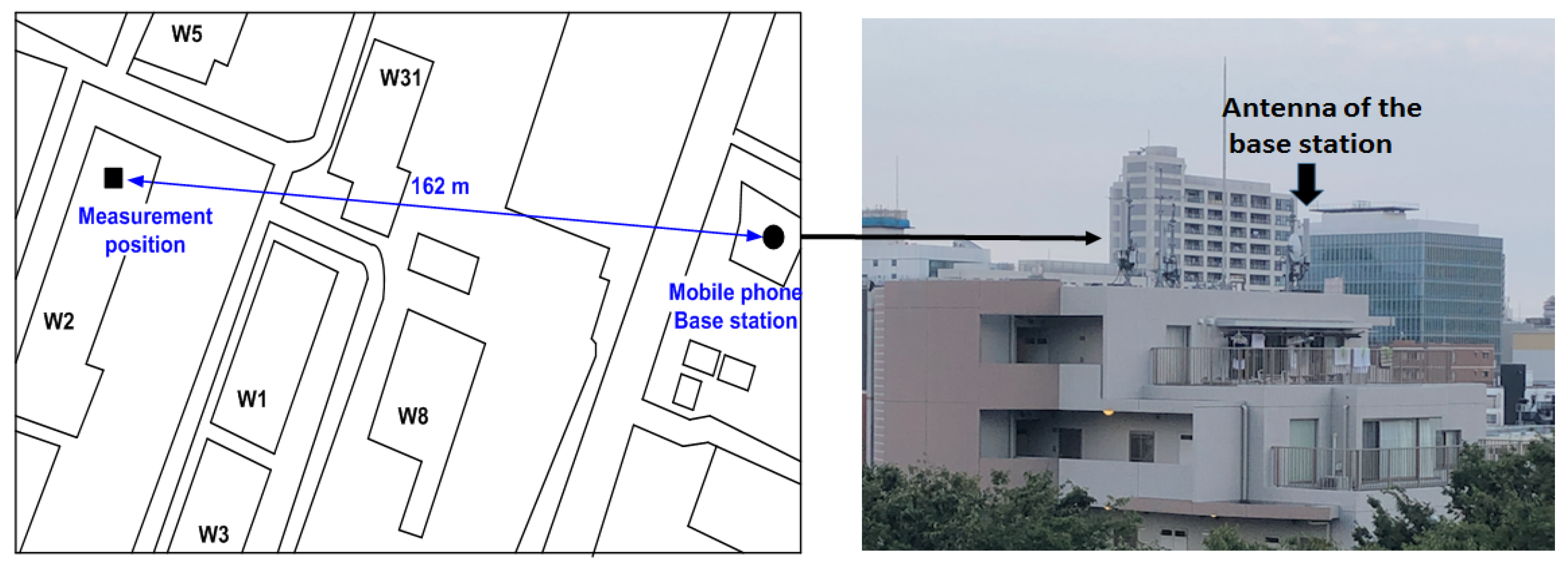
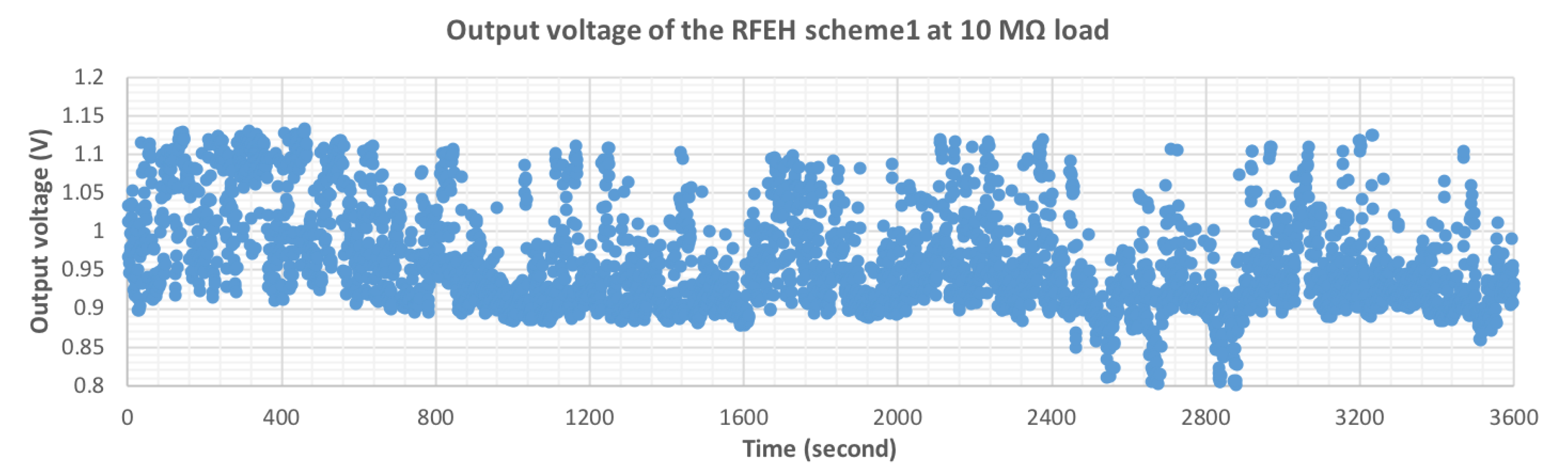
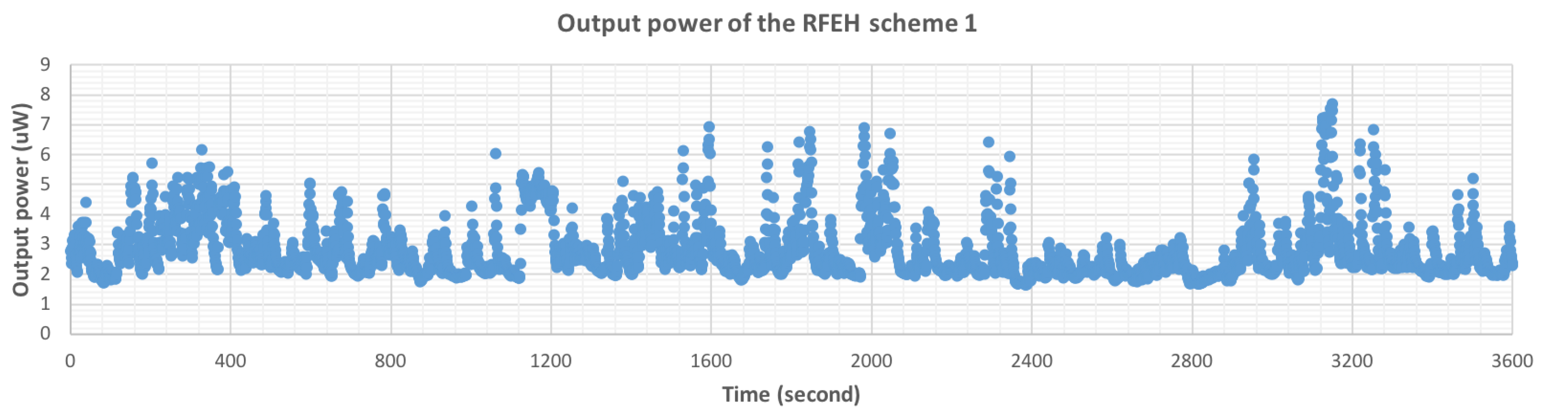
4.2. RF Energy Harvesting from the Environment

Figure 19 shows the measurement set up in an office room at a laboratory in the University of Electro-Communications, Tokyo, Japan. The map of the measurement position is shown in Figure 2. The input power is measured by a signal analyzer Agilent CXA N900A. Output voltages are measured by a digital multimeter DMM7510, and the data is stored on a computer. The time resolution of the measurement with the multimeter is set to a second.
The level of RF signal in the ambient environment is not stable and continuously changes depending on many factors such as position, time, and weather. To comprehensively express the performance of the proposed RFEH system when harvesting RF signal, it is essential to measure and store data over a long evaluation time. This data is analyzed, and the performance of the system is studied. In the paper, all the measurement results with ambient RF signals were performed in real-time, and distribution data are presented.
Figure 20 shows the measured input power measured for an hour. The distribution of the input power is shown in Figure 21. From the figures, it can conclude that the general LTE level at the measurement position is −19.4 dBm, and the average input power is −18 dBm.
In the first measurement, the output voltage of the RFEH system when harvesting LTE signal is measured at 100 μ F capacitor and open load, as shown in Figure 22. The figure indicates that the voltage at the capacitor is charged to 1 V after 15 s.
P C in the figure stands for power charged at capacitor which is calculated by Equation (7)
P C = C V o u t 2 2 V o u t 1 2 2 t 2 t 1 = C V o u t 2 2 V o u t 1 2 2 Δ t
In the next measurement, the performance of the proposed RFEH system with different load resistors is measured. Figure 23 shows the measured output voltage at 10 M Ω load of the RFEH scheme 1 as measured for an hour. The output voltages are in the range of 0.8–1.15 V.
Figure 24 and Figure 25 show the measured output power and its distribution of the proposed RFEH scheme 1 as measured for an hour. As shown in the Figure, the general output power that the proposed RFEH scheme 1 generated is 2.09 μ W, and the average power for the one-hour measurement corresponds to 2.77 μ W.
In the next measurement, the stable operation and efficiency of the proposed RFEH system are tested and measured for 24 h. Figure 26 shows output power over every second of the RFEH scheme 2. The proposed system generates a 2.75 μ W average DC power as measured for 24 h. The total power received by the proposed RFEH system in a day is 0.238 J.
As mentioned above, the level of the LTE signal in the real environment continuously changes, causing the output power of the RFEH system changes. Therefore, the efficiency in the case measured in the ambient environment is calculated by the distributions of input RF power and output DC power. From Figure 21 and Figure 25, the PCE of the RFEH system is 18% at a level of −19.4 dBm input power.
Compared with the 1 μ W output power that the system generates with the CW signal, 2.77 μ W output power obtained by harvesting the RF signal from the ambient environment shows significantly better results. The results prove the efficient operation of the proposed RFEH systems when performs in the ambient environment.
Figure 27 presents the recent state-of-the-art results obtained in ambient RF energy harvesting. Table 1 shows a comparison of the results between studies on ambient RFEH and those obtained from the present study. As observed from the figure and table, we conclude that in the present study, the proposed RFEH harvests the highest output power at the same input power level when compared to the other studies.
In Figure 27, the wireless energy harvester [20], which is a high Q system, generates 0.2 μ W at −30 dBm input CW signal but that at −18.6 dBm input power of real Wifi signal is 3.3 nW. Whereas, to ensure a wide bandwidth, in the proposed system, the Q factor is abandoned. Therefore, the resulting output power of the system when harvesting the CW signal is 1 μ W at −20 dBm input power. At the same level, when the system scavenges the LTE signal, the output power of the system is boosted to 2.77 μ W. The results prove that the structure of the RFEH system proposing in this study is effective in environmental performance.

5. Conclusions

We herein proposed the design of an RFEH system to harvest an RF signal from an ambient environment. The moderate Q factor is designed to have the necessary bandwidth for scavenging an ambient RF signal. A DTMOS CCR with floating sub-circuits is proposed to achieve a high conductance configuration for improving efficiency. A wideband matching between antenna and rectifier is obtained to guarantee the bandwidth of the RF signal. A simple wire dipole antenna is designed to match with the rectifier. Two structures of the RF energy harvesting system are proposed. The proposed systems obtained 2.77 μ W at an input power of approximately −20 dBm by scavenging an environmental LTE mobile phone signal with 15 MHz bandwidth at 952 MHz frequency. The total power that the system harvested for a day accounts for 0.238 J. The obtained results indicate the highest performance at the input level range when compared to the other studies, thereby demonstrating that the proposed RFEH system has good potential for battery-less IoT applications.

Author Contributions

Main investigation, T.-L.N.; Validation, Y.S.; Principle supervisor, K.I.

Funding

This research is funded by JST-CREST Grant Number JPMJCR16Q1.

Acknowledgments

The research is also supported by VLSI Design and Education center (VDEC), the University of Tokyo in collaboration with Synopsys, Inc. and Cadence Design Systems, Mentor Inc.

Conflicts of Interest

The authors declare no conflict of interest.

Appendix A

Figure A1 presents a detailed schematic of the RFEH system, where all components and parasitic components are included.
Figure A1. The equivalent of the RFEH scheme 2.
Electronics 08 01173 g0a1
Table A1 shows the definitions and values of words in the Figure A1.
Table A1. Definition table.
WordDefinitionValueWordDefinitionValue
L M Inductor for matching4.1 nH Q L M Quality factor of L M 40
C M Capacitor for matching6.5 pF Q C M Quality factor of C M 400
WWidth of transmission line L T L Length of transmission line
L B Parasitic inductor of bonding wire Q B Quality factor of bonding wire64
C P Parasitic capacitor of pad in PCB board0.01 pF C E S D Parasitic capacitor of pad on chip2.1 pF

References

  1. Lu, X.; Wang, P.; Niyato, D.; Kim, D.I.; Han, Z. Wireless Networks with RF Energy Harvesting: A contemporary Survey. IEEE Commun. Surv. Tutor. 2015, 17, 757–789. [Google Scholar] [CrossRef]
  2. Kim, S.; Vyas, R.; Bito, J.; Niotaki, K.; Collado, A.; Georgiadis, A.; Tentzeris, M.M. Ambient RF Energy Harvesting Technologies for Self-Sustainable Standalone Wireless Sensor Platforms. Proc. IEEE 2014, 102, 1649–1666. [Google Scholar] [CrossRef]
  3. Kitazawa, S.; Ban, H.; Kobayashi, K. Energy Harvesting from Ambient RF Sources. In Proceedings of the 2012 IEEE MTT-S International Microwave Workshop Series on Innovative Wireless Power Transmission: Technologies, Systems, and Applications, Kyoto, Japan, 10–11 May 2012; pp. 39–42. [Google Scholar]
  4. Furuta, T.; Ito, M.; Nambo, N.; Itoh, K.; Noguchi, K.; Ida, J. The 500 MHz band low power rectenna for DTV in the Tokyo area. In Proceedings of the 2016 IEEE Wireless Power Transfer Conference (WPTC), Aveiro, Portugal, 5–6 May 2016. [Google Scholar]
  5. Pinuela, M.; Micheson, P.D.; Lucyszyn, S. Ambient RF Energy Harvetsing in Urban and Semi-Urban Environments. IEEE Trans. Microwave Theory Tech. 2013, 61, 2715–2726. [Google Scholar] [CrossRef]
  6. Arrawatia, M.; Baghini, M.S.; Kumar, G. RF Energy Harvesting System from Cell Towers in 900 MHz Band. In Proceedings of the National Conference on Communications, Bangalore, India, 28–30 January 2011; pp. 1–5. [Google Scholar]
  7. Mikeka, C.; Arai, H.; Georgiadis, A.; Collado, A. DTV Band Micropower RF Energy Harvesting Circuit Architecture and Performance Analysis. In Proceedings of the IEEE International Conference on RFID-Technology and Appications, Sitges, Spain, 15–16 September 2011; pp. 561–567. [Google Scholar]
  8. Kitazawa, S.; Kanoda, H.; Hanazawa, M.; Ano, S.; Ban, H.; Kobayashi, K. A Study on RF energy harvesting from three broadcasting and communication frequency bands. IEICE Tech. Rep. 2013, 113, 53–58. [Google Scholar]
  9. Kotani, K.; Ito, T. HIgh efficiency CMOS rectifier circuit with self-Vth-cancellation and power regulation functions for UHF RFIDs. In Proceedings of the IEEE Asian Solid-State Circuit Conference, Jeju, Korea, 12–14 November 2007; pp. 119–122. [Google Scholar]
  10. Kotani, K.; Ito, T. High efficiency Differential-Drive CMOS Rectifier for UHF RFIDs. IEEE J. Solid-State Circuits 2009, 44, 3011–3018. [Google Scholar] [CrossRef]
  11. Theilmann, P.T.; Presti, C.D.; Kelly, D.J.; Asbeck, P.M. A μW Complementary Bridge Rectifier With Near Zero Turn-on Voltage in SOS CMOS for Wireless Power Supplies. IEEE Trans. Circuit Syst. 2012, 59, 2111–2124. [Google Scholar] [CrossRef]
  12. Wong, S.Y.; Chen, C.C. Power efficient multi-stage CMOS rectifier design for UHF RFID tags. ELSEVIER INTEGRATION VLSI J. 2011, 44, 242–255. [Google Scholar] [CrossRef]
  13. Kamalinejad, P.; Keikhosravy, K.; Mirabbasi, S.; Leung, V.C.M. An Efficiency Enhancement Technique for CMOS Rectifier with Low Start-Up Voltage for UHF RFID Tags. In Proceedings of the IEEE International Green Computing Conference Proceedings, Arlington, VA, USA, 27–29 June 2013; pp. 1–6. [Google Scholar]
  14. Liu, Z.; Zhong, Z.; Guo, Y.X. High-Efficiency Triple-band Ambient RF Energy Harvesting for Wireless Body Sensor Network. In Proceedings of the IEEE IMWS-Bios, London, UK, 8–10 December 2014; pp. 1–3. [Google Scholar]
  15. Tung, N. Multi-band Ambient RF Energy Harvesting Rectifier for Autonomous Wireless Sensor Networks. In Proceedings of the 2016 IEEE Region 10 Conference (TENCON), Singapore, 22–25 November 2016; pp. 3736–3739. [Google Scholar]
  16. Arrawatia, M.; Baghini, M.S.; Kumar, G. Broadband RF Energy Harvesting System covering CDMA, GSM900, GSM1800, 3G Bands with Inherent Impedance Matching. In Proceedings of the IEEE IMS, San Francisco, CA, USA, 22–27 May 2016; pp. 1–3. [Google Scholar]
  17. Stoopman, M.; Keyrouz, S.; Visser, H.J.; Phillips, K.; Serdijn, W.A. Co-Design of a CMOS Rectifier and Small Loop Antenna for Highly Sensitive RF Energy Harvesters. IEEE J. Solid-State Circuits 2014, 49, 622–634. [Google Scholar] [CrossRef]
  18. Kang, J.; Chiang, P.Y.; Natarajan, A. A 3.6 cm2 Wirelessly-Powered UWB SoC with −30.7 dBm Rectifier Sensitivity and Sub-10cm Range Resolution. In Proceedings of the IEEE Radio Frequency Integrated Circuits Symposium, Phoenix, AZ, USA, 17–19 May 2015; pp. 255–258. [Google Scholar]
  19. Le, T.; Mayaram, K.; Fiez, T. Efficient Far-Feild Radio Frequency Energy Harvesting for Passively Powered Sensor Networks. IEEE J. Solid-State Circuits 2008, 43, 1287–1301. [Google Scholar] [CrossRef]
  20. Sadagopan, K.R.; Kang, J.; Ramandass, Y.; Natarajan, A. A 960pW Co-Integrated-Antenna Wireless Energy Harvester for Wifi Backchannel Wireless Powering. In Proceedings of the ISSCC 2018, San Francisco, CA, USA, 11–15 February 2018; pp. 136–137. [Google Scholar]
  21. Bolos, F.; Blanco, J.; Collado, A.; Georgaiadis, A. RF Energy Harvesting From Multi-Tone and Digitally Modulated Signals. IEEE Trans. Microw. Theory Tech. 2016, 64, 1918–1927. [Google Scholar] [CrossRef]
  22. Valenta, C.R.; Morys, M.M.; Durgin, G.D. Theoretical Energy-Conversion Efficiency for Energy-Harvesting Circuits Under Power-Optimized Waveform Excitation. IEEE Trans. Microw. Theory Tech. 2015, 63, 1758–1767. [Google Scholar] [CrossRef]
  23. Collado, A.; Georgiadis, A. Optimal Waveforms for Efficient Wireless Power Transmission. IEEE Microwave Wirel. Compon. Lett. 2014, 24, 354–356. [Google Scholar] [CrossRef]
  24. Lee, T.H. Passive RLC networks. In The Design of CMOS Radio-Frequency Integrated Circuits, 2nd ed.; Cambridge University Press: Cambridge, UK, 2004. [Google Scholar]
  25. Niknejad, M.A. Resonance and Impedance Matching. In Electromanegtics for High-Speed Analog and Digital Communication Circuits; Cambridge University Press: Cambridge, UK, 2007. [Google Scholar]
  26. Assaderaghi, F.; Sinitsky, D.; Parke, S.; Bokor, J.; Ko, P.K.; Hu, C. A dynamic threshold voltage MOSFET (DTMOS) for very low voltage operation. IEEE Electron Device Lett. 1994, 15, 510–512. [Google Scholar] [CrossRef]
  27. Chouhan, S.; Halonen, K. The design and Implementation of DTMOS biased all PMOS rectifier for RF energy harvesting. In Proceedings of the IEEE International New Circuits and Systems Conference, Trois-Rivieres, QC, Canada, 22–25 June 2014; pp. 444–447. [Google Scholar]
  28. Chouhan, S.; Halonen, K. The DTMOS based UHF RF to DC conversion. In Proceedings of the IEEE International Conference on Electronics, Circuits, and Systems, Abu Dhabi, UAE, 8–11 December 2013; pp. 629–632. [Google Scholar]
  29. Asli, A.N.F.; Wong, Y.C. -23.5 dBm sensitivity, 900 MHz differential-drive rectifier. In Proceedings of the International SoC Design Conference, Seoul, Korea, 5–8 November 2017; pp. 79–80. [Google Scholar]
  30. Yamamoto, Y.; Makiyama, H.; Shinohara, H.; Iwamatsu, T.; Oda, H.; Kamohara, S.; Sugii, N.; Yamaguchi, Y.; Mizutani, T.; Hiramoto, T. Ultralow-voltage operation of Silicon-on-Thin-BOX(SOTB) 2Mbit SRAM down to 0.37V ultilizing adaptive back bias. In Proceedings of the Symposium on VLSI Technology, Kyoto, Japan, 12–14 June 2013; pp. T212–T213. [Google Scholar]
  31. Makiyama, H.; Horita, K.; Iwamatsu, T.; Oda, H.; Sugii, N.; Inoue, Y.; Yamamoto, Y. Design Consideration of 0.4V-Operation SOTB MOSFET for Super Low Power Application. In Proceedings of the IEEE International Meeting for Future of Electron Devices, Osaka, Japan, 19–20 May 2011. [Google Scholar]
  32. Linh, N.T.; Takahashi, S.; Sato, Y.; Ishibashi, K. RF Energy Harvesting using Cross-Couple Rectifier and DTMOS on SOTB with Phase Effect of paired RF inputs. In Proceedings of the IEEE ECTI Conference, Chiang Rai, Thailand, 18–21 July 2019. [Google Scholar]
  33. Trung, V.N.; Ishikawa, R.; Ishibashi, K. 83nJ/bit Transmitter using code modulated synchronized-OOK on 65nm SOTB for normally-off wireless sensor networks. IEICE Trans. Electron. 2018, E101-C.472, 472–479. [Google Scholar]
Figure 1. Measured spectrum of RF signals at the measurement position: (a) Spectrum of RF signals and (b) Magnified spectrum of the 952 MHz signal.
Electronics 08 01173 g001
Figure 2. Map of the measurement position and picture of mobile phone antenna.
Electronics 08 01173 g002
Figure 3. Dynamic threshold MOSFET (DTMOS) cross-coupled rectifier with floating sub-circuits.
Electronics 08 01173 g003
Figure 4. Simulated DC level-up amount ( Δ V D C ) from the floating sub-circuit.
Electronics 08 01173 g004
Figure 5. Simulated IV characteristic of the DTMOS diode, body-tide-to-source MOSFET (BTMOS) diode, DTMOS cross-coupled rectifier (CCR) configuration, and DTMOS CCR with floating sub-circuits configuration.
Electronics 08 01173 g005
Figure 6. N-stage CCR with floating sub-circuits: (a) block diagram of the circuit, and (b) simulated dependence of Q factor on the number of rectifier stages.
Electronics 08 01173 g006
Figure 7. Proposed RF energy harvesting (RFEH) systems: (a) rectifier micrograph, (b) the RFEH scheme 1, and (c) the RFEH scheme 2.
Electronics 08 01173 g007
Figure 8. The equivalent circuit of the RFEH system scheme 1.
Electronics 08 01173 g008
Figure 9. Measured impedance and S11 of the RFEH scheme 1: (a) Impedance, (b) S11.
Electronics 08 01173 g009
Figure 10. Equivalent of the RFEH scheme 2.
Electronics 08 01173 g010
Figure 11. Matching in smith chart for the RFEH scheme 2.
Electronics 08 01173 g011
Figure 12. Simulated and measured reflection coefficients at: (a) Port 1 and (b) Port 2.
Electronics 08 01173 g012
Figure 13. Measured impedance and S11 of the RFEH scheme 2: (a) Impedance and (b) S11.
Electronics 08 01173 g013
Figure 14. Measured and simulated output of the RFEH system with the signal generator when the system is excited by continuous sine wave (CW) signal: (a) Output voltages and (b) power conversion efficiency (PCE) at different loads and input power.
Electronics 08 01173 g014
Figure 15. Measurement setup in an anechoic chamber.
Electronics 08 01173 g015
Figure 16. Measurement results of the proposed RFEH system in an anechoic chamber: (a) Output voltages at 10 M Ω with CW signal and modulated signals and (b) PCE with a CW signal.
Electronics 08 01173 g016
Figure 17. Measured PCE of the RFEH system in different loads in the anechoic chamber: (a) at −20 dBm input power, and (b) at −10 dBm input power.
Electronics 08 01173 g017
Figure 18. Measured dependence of PCE on Peak-to-Average-Power ratio (PAPR) of RF signal.
Electronics 08 01173 g018
Figure 19. Measurement condition in the office room.
Electronics 08 01173 g019
Figure 20. Input power as measured for 1 h.
Electronics 08 01173 g020
Figure 21. Distribution of input power as measured for 1 h.
Electronics 08 01173 g021
Figure 22. Output voltage of the RFEH scheme 2 at a load 100 μ F capacitor.
Electronics 08 01173 g022
Figure 23. Output voltage of scheme 1 at 10 M Ω loads as measured for 1 h.
Electronics 08 01173 g023
Figure 24. Output power of scheme 1 at 82 k Ω loads as measured for 1 h.
Electronics 08 01173 g024
Figure 25. Distribution of output power of scheme 1 at 82 k Ω loads as measured for 1 h.
Electronics 08 01173 g025
Figure 26. Output power of scheme 2 at 100 k Ω loads as measured for 24 h.
Electronics 08 01173 g026
Figure 27. Recent state-of-the-art in ambient RF energy harvesting.
Electronics 08 01173 g027
Table 1. Comparison table.
This WorkKitazawa 2013 [8]Stoopman 2014 [17]Furuta 2016 [4]Sadagopan 2018 [20]
Technology65 nm SOTB CMOSDiode HSMS285C90 nm CMOSDiode HSMS285CGP 65 nm CMOS
Rectifier stages3-stage DTMOS CCR with floating sub-circuit2-stage charge pump5-stage CCR1-stage and 2-stage Cockcroft- Walton6-stage CCR
FrequencyLTE 950 MHz bandV-High (205–225) MHz, DTV (465–545) MHz, BTS (850–900) MHz868 MHzDTV 500 MHz bandWifi 2.4 GHz band
Sensitivity @ Input power, Load0.9 V @ −20 dBm, 10 M Ω na1 V @ −27 dBm, R L = 0.8 V * @ −15 dBm, 39 k Ω 1 V @ −36 dBm, R L = Primary mode, 1 V @ −33 dBm, R L = Cold start
Max PCE with sine wave signal57% @ −10 dBm9.1% @ −20 dBm40% @ −17 dBm48.9%@ −15 dBmna
Output power @ input power with RF signal from ambient environment2.77 μ W @ −19.4 dBm1.9 μ W * @ −15 dBm *0.16 μ W * @ −4.6 dBm22.53 μ W * @ −13 dBm3.3 nW * @ −18.6 dBm *
*: Calculated from graph.

