Article

A Subthreshold Bootstrapped SAPTL-Based Adder Design

1
Institute of Microelectronics of Chinese Academy of Sciences, Beijing 100029, China
2
The EDA center of Chinese Academy of Sciences, Beijing 100029, China
3
Beijing Key Laboratory of 3D & Nano IC Design Automation Technology, Beijing 100029, China
4
School of Electronic, Electrical and Communication Engineering, University of Chinese Academy of Sciences, Beijing 100049, China
5
Key Laboratory of Microelectronic Devices & Integrated Technology, Chinese Academy of Sciences, Beijing 100029, China
*
Author to whom correspondence should be addressed.
Electronics 2019, 8(10), 1161; https://doi.org/10.3390/electronics8101161
Submission received: 11 September 2019 / Revised: 9 October 2019 / Accepted: 10 October 2019 / Published: 12 October 2019
(This article belongs to the Section Microelectronics)

Abstract

:
This paper proposes a 16 bit subthreshold adder design using bootstrapped sense amplifier-based pass transistor logic (bootstrapped SAPTL) to overcome serious performance degradation and enhance the immunity to process variations in the subthreshold region. Through employing a bootstrapped sense amplifier including a voltage boosting part and adopting an adder architecture based on bootstrapped SAPTL, significant improvements in performance and energy efficiency can be achieved. A case study of 16 bit adders in SMIC 130 nm technology demonstrated that the proposed adder outperformed other works in terms of performance, energy consumption, and energy efficiency. Furthermore, the statistical results of the Monte Carlo analysis proved the proposed adder’s significant enhancement of robustness against process and temperature variations. At 0.3 V (TT corner, 25 °C), the proposed 16 bit adder achieved improvements of 72% in performance and 8% in energy savings, as well as a 74% reduction in energy-delay production as compared with the current design.

1. Introduction

The subthreshold technique is becoming increasingly popular with the fast growth in the market for ultra-low-power applications, such as Internet of Things (IoT), wearable devices, and biomedical implants [1,2,3]. The working principle is to scale the supply voltage below the threshold voltage, and the operation current in this region [4] is given as:
I s u b = W L μ 0 C o x ( n 1 ) exp ( V g s V t h n V T ) ( 1 exp ( V d s V T ) )
This equation indicates that I s u b has an exponential relationship with V g s and V t h . Therefore, the operation current sharply decreases with a descending supply voltage [5,6] and is sensitive to process variations [7,8,9], which limits the practical usage of subthreshold circuits.
The adder circuitry, as a frequently used arithmetic unit in many ultra-low-power applications [10,11], also suffers from these problems in the subthreshold region. Numerous studies have been conducted on subthreshold adder design. One method is to adopt new devices like FinFET [12] and FD-SOI [13], which are still immature. Another method is to modify the basic structure of the full adder cell [14,15,16,17]. Pass transistors and transmission gates are usually used in this method for a smaller area and lower power, which has a finite effect on improving the performance. In addition, using fast adder architecture optimized at the logic level is also a viable method to enhance the circuit speed [18,19], such as carry look-ahead adder (CLA) design [15,18,20]. But these works mainly focus on the structure design of gate-level circuits, like an XOR gate, which still have difficulty in achieving an acceptable level of performance in the subthreshold region. Additional circuits for a CLA also bring about a large area and energy overhead. Furthermore, effective solutions for reducing the effect of process variations are often lacking in subthreshold adder designs.
Sense amplifier-based pass transistor logic (SAPTL) [21] can be introduced here for simultaneous optimization of performance and energy dissipation [22]. It is a logic style which performs logical operations through a pass transistor network (PTN) without DC leakage paths and resumes the signals by employing a sense amplifier (SA). The differential amplification mechanism and the internal cross-coupled latch contribute to a stronger robustness against variations. However, there still exist two main drawbacks when applying SAPTL to subthreshold adder design: 1) the performance of the SA degrades severely because its input differential signals are generated by a PTN and are not full swing; and 2) there is a lack of an area-saving method to use SAPTL in the adder circuit. In Reference [23], a SAPTL circuit was directly used to replace full adders, which needed many SAs and resulted in large overhead. In Reference [24], SAPTL was adopted to generate all data outputs of an 8 bit adder and each output corresponded to a PTN stack and an SA, leading to a large area. In Reference [25], SAPTL was used for computing each carry signal in the 4 bit CLA block, but it was still too complicated and needed eight SAs. Moreover, no efforts were made to improve the performance of the SAs for subthreshold operation in these works.
To overcome the above problems of SAPTL-based subthreshold adders, this work proposes a subthreshold adder design based on a bootstrapped SAPTL circuit. The contributions of this paper are listed as follows: 1) we present a bootstrapped sense amplifier to improve the performance of a subthreshold SAPTL circuit, with six additional transistors and a PMOS capacitor; and 2) we introduce an adder architecture that adopts bootstrapped SAPTL in each 4 bit adder block to accelerate the carry chain with low overhead.
The remainder of this paper is organized as follows. Section 2 introduces the proposed bootstrapped sense amplifier circuit and the adder architecture design using SAPTL. Section 3 describes the experiment and results. Section 4 concludes this paper.

2. Proposed Subthreshold Adder Design

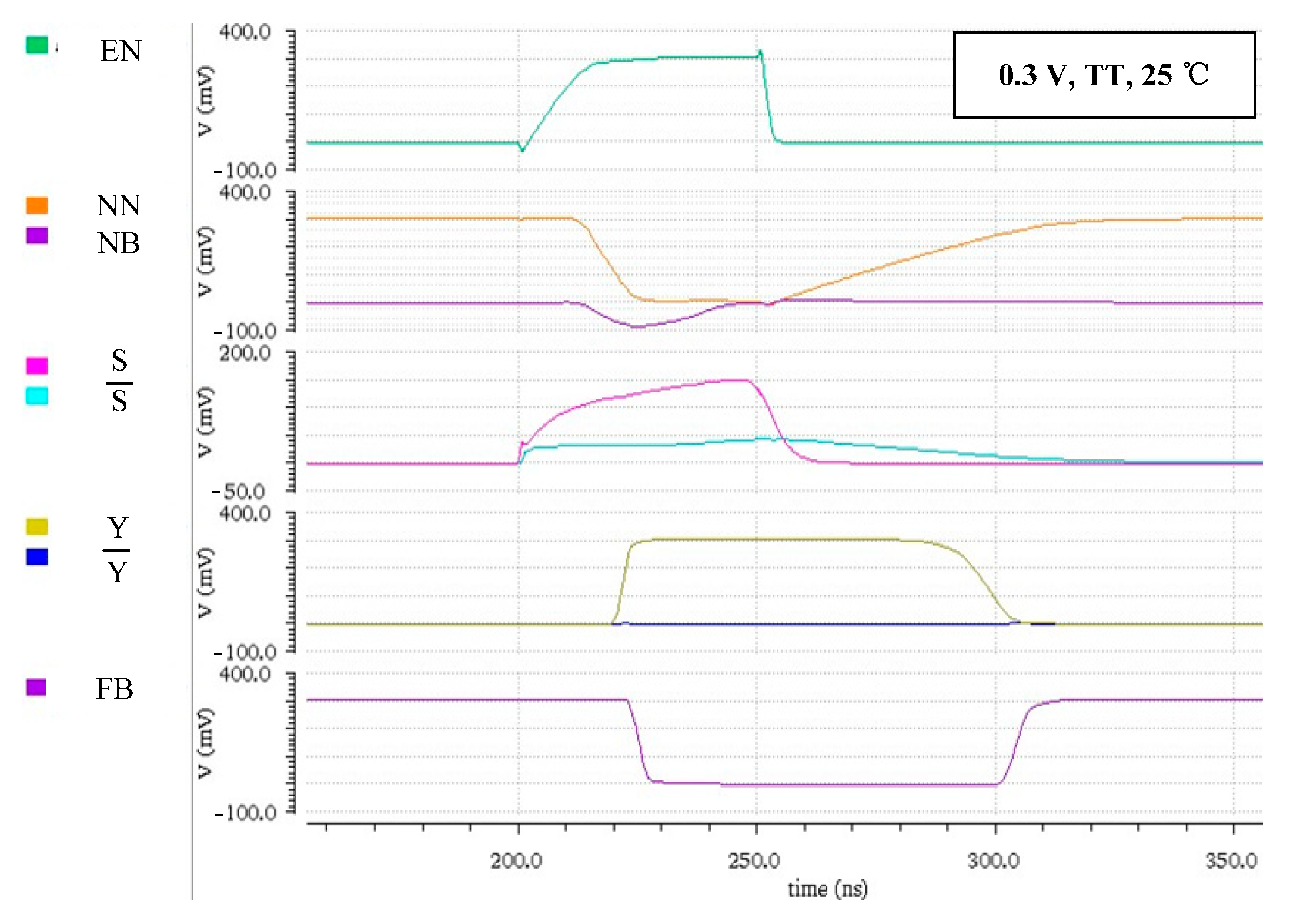
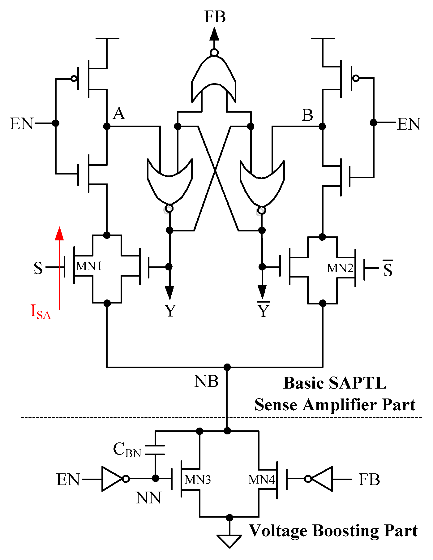
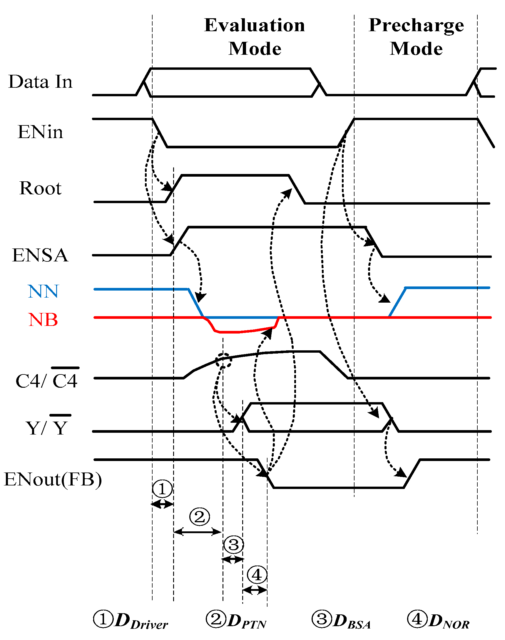
2.1. Bootstrapped Sense Amplifier

As shown in Figure 1, a bootstrapped sense amplifier (BSA) was partitioned into two parts: the basic SAPTL sense amplifier part and the voltage boosting part. This BSA can boost V g s of the input transistors dynamically, thus increasing the operation current and improving the performance.
We take the condition that V S > V S ¯ , for example, and the delay of the basic sense amplifier in the evaluation mode [26] can be expressed as:
D S A = k 1 C A V d d I S A + k 2 I A I B
where k 1 and k 2 are fitting parameters, C A is the capacitor at node A, which is fixed in general, and I S A is the operation current of MN1. Compared to the first term, the second term can be negligible in the subthreshold region [27]. Therefore, the speed of the SA principally depends on I S A . However, since V S is the output of PTN and is normally much lower than V d d , I S A is very weak and extremely limits the speed of SA. The voltage boosting part was only applied here to boost the V g s of MN1 and, thus, enlarge I S A to enhance the speed.
Figure 2 presents the simulation waveforms of the BSA circuit at 0.3 V (TT corner, 25 °C).
As can be seen, the BSA has two operation phases:
  • EN = 0. BSA is in the pre-charge mode. V A = V B = 1 and, thus, the outputs V Y = V Y ¯ = 0. FB = 1. MN3 is on and MN4 is off, making V N N = 1 and V N B = 0 . A voltage equal to V d d is thus applied across C B N .
  • EN = 1. BSA is in the evaluation mode. Before the differential inputs become valid, V N N = 0 and MN3 turns off, then the capacitive coupling through C B N will force V N B to be boosted below 0. After the input signals become valid, V g s of MN1 is thus enlarged effectively and makes MN1 faster. At the same time, V b s of MN1 is also increased and, hence, V t h of MN1 is reduced slightly by forward body biasing, accelerating MN1 further. Either V A or V B will be pulled down below 0 to generate two inverse outputs through the cross-coupled latch. Then FB will turn to 0 and turn on MN4 to reset the value of V N B to 0. This procedure is to prevent the undesired leakage of MN2 from pulling V B down because V g s of MN2 is larger than 0 after the evaluation is finished if V N B is not reset.
The boosting part brings about extra energy overhead, while it can be offset by lower leakage energy due to the smaller delay. C B N is realized using a PMOS capacitor, with its drain, source, and body terminals connected together. The minimum value of V N B depends on C B N . A larger capacitor produces smaller V N B , with stronger speed enhancement and higher energy consumption. A too-small capacitor cannot offer enough performance improvement. The value of C B N should be set through simulation to provide a minimum energy-delay product. In this work, the PMOS capacitor was sized W/L = 1.1 μm/1.1 μm to provide a C B N of approximately 10 fF.

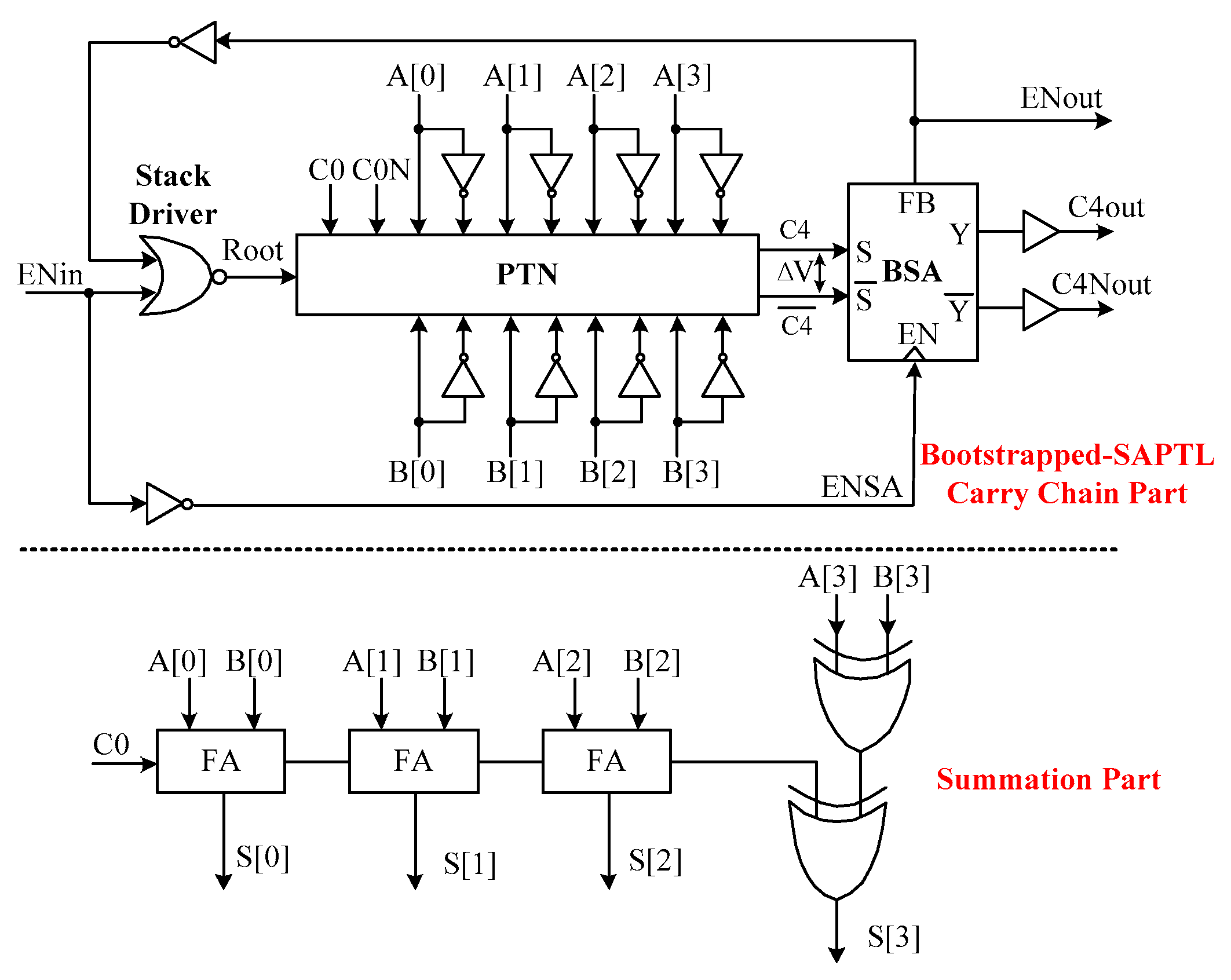
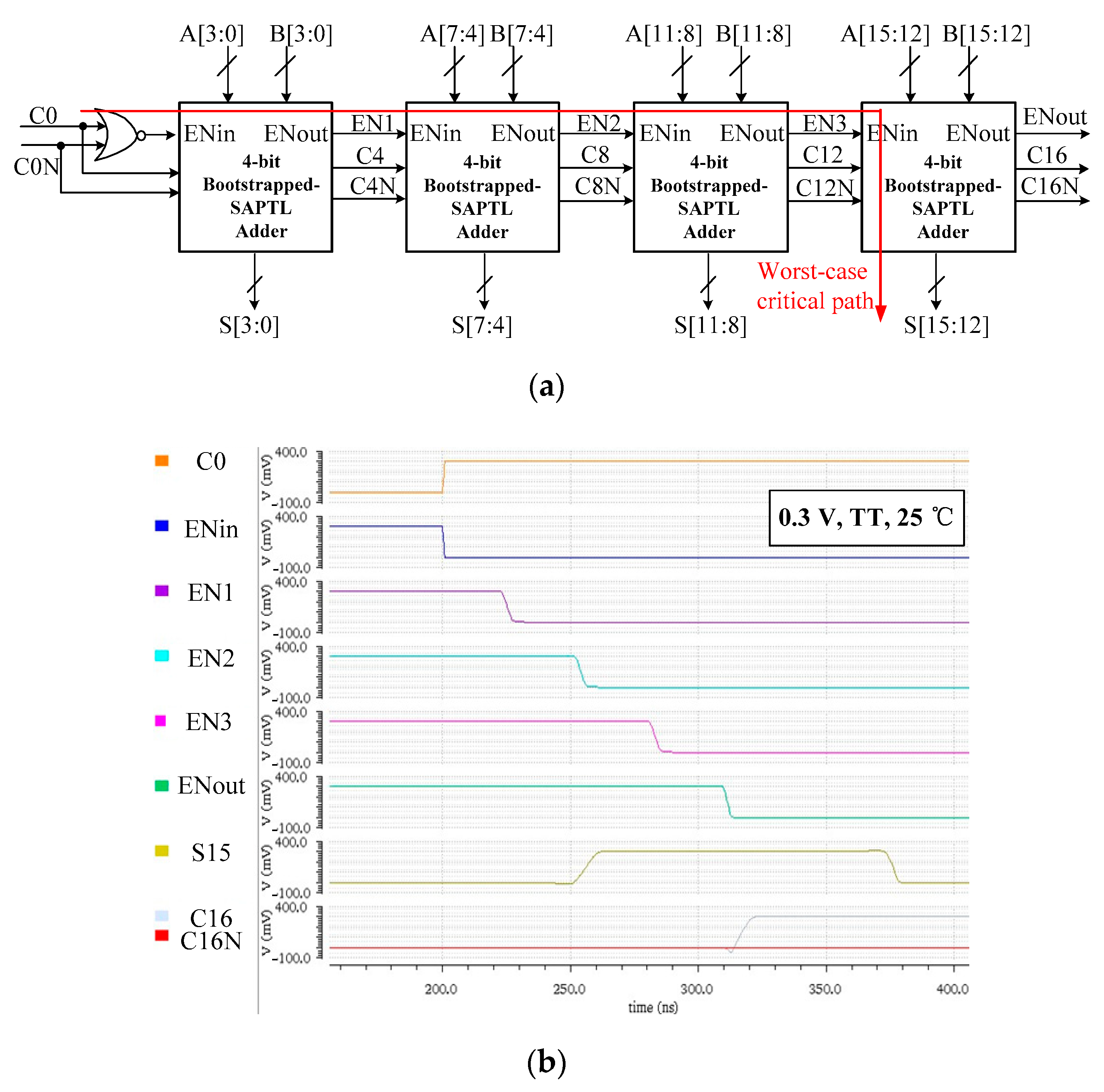
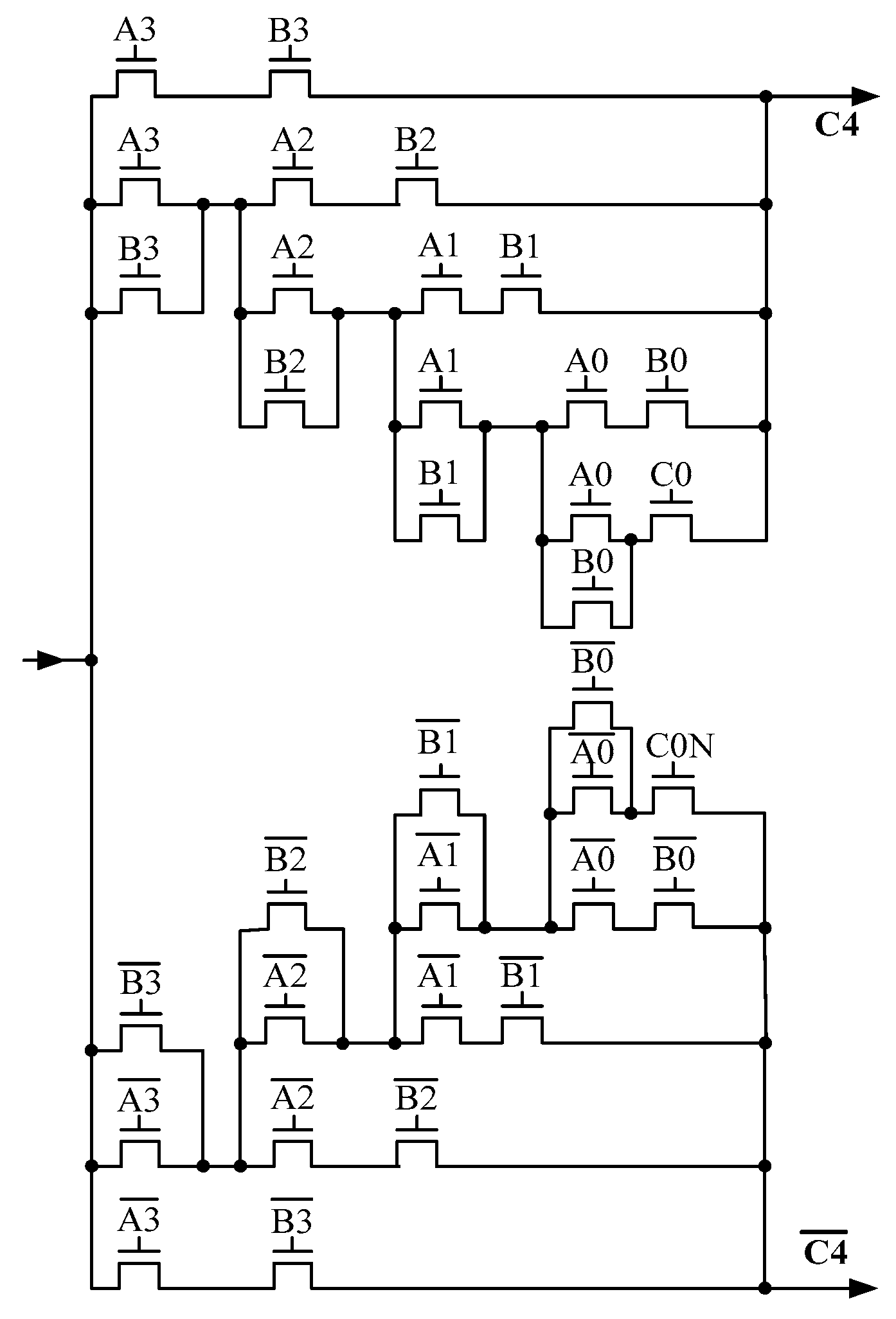
2.2. The Adder Architecture Based on Bootstrapped-SAPTL

Figure 3 illustrates the adder architecture based on bootstrapped SAPTL. The 4 bit adder block can be divided into the carry chain part, realized by bootstrapped SAPTL, and the summation part using serial full adders. This architecture can take full advantage of the bootstrapped SAPTL technique to improve the performance, while minimizing the extra overhead.
The bootstrapped SAPTL carry chain part does not generate any intermediate carry signal. Only one PTN stack and one BSA are needed and, hence, the additional area overhead is under control. The structure of the PTN is simplified and has a minimum transistor number of 34, as shown in Figure 4.
The timing diagram of the bootstrapped SAPTL circuit is illustrated in Figure 5.
The delay of the carry chain part is as follows:
D c a r r y = D D r i v e r + D P T N + D B S A + D N O R
where D D r i v e r is the rising delay of the stack driver and D P T N is the delay for the PTN stack to develop a valid differential voltage. D B S A can be expressed by Equation (2). D B S A was largely decreased and, thus, is not conspicuous in Figure 5. In addition to using BSA to improve the performance, the stack driver adopts low-threshold PMOS transistors (plvt) to accelerate the pull-up operation to reduce D D r i v e r and the PTN stack adopts low-threshold NMOS transistors (nlvt) [28] with minimum size to increase the on/off current ratio to reduce D P T N . Using plvt will lead to a certain increase in energy consumption but can decrease the delay effectively, while the usage of nlvt in the PTN can reduce the delay with almost no extra energy.
As for the summation part, its speed is unrelated to the carry chain part and the delay of the summation part ( D s u m ) is always larger than D c a r r y . Figure 6 illustrates the D c a r r y and D s u m in the worst case with supply voltage scaling in SMIC 130 nm technology.
It can be observed that the ratio of D c a r r y to D s u m ranges from 41% to 50%. In fact, the overall worst-case delay of a multi-bit adder composed of n 4 bit bootstrapped SAPTL adder blocks should be expressed as follows:
D w o r s t c a s e = ( n 1 ) D c a r r y + D s u m   , n 1
Since D c a r r y is the main component in D w o r s t c a s e , the summation part can adopt a modified full adder structure with relatively slower speed to reduce power dissipation. The structures of the full adder and XOR gate in Reference [15] were adopted in this work.
For a ripple-carry adder composed of n serial 4 bit adder blocks, its delay was approximately equal to n · D s u m and, thus, the ratio of reduction in the delay through the use of the proposed 4 bit bootstrapped SAPTL adder blocks is as follows:
r = 1 ( n 1 ) D c a r r y + D s u m n D s u m = ( 1 1 n ) ( 1 D c a r r y D s u m )  
It is evident that r goes up with increasing n. Therefore, it is suggested to apply the proposed adder architecture to adder circuits with higher bits to enhance the speed. A 16 bit bootstrapped SAPTL adder with n = 4 can offer an r of 37.50–44.25%, while a 32 bit bootstrapped SAPTL adder increases r to 43.75–51.63%.

3. Experiment Results

The case of 16 bit adders in SMIC 130 nm technology was studied to evaluate the proposed adder design. This adder consisted of four serial 4 bit bootstrapped SAPTL adder blocks, as depicted in Figure 7a. The worst-case critical path was plotted using a red line. The input signals are set with a 1 ns rising/falling time. Figure 7b shows the transient simulated waveform at 0.3 V (TT corner, 25 °C).
Based on the sizing method in Reference [29], the proposed adder was sized through simulations in SMIC 130 nm technology. The transistor parameter settings of the proposed adder are shown in Table 1. All the NMOS transistors used in this work were sized with the minimum channel width and length (W/L = 150 nm/130 nm) to utilize the reverse narrow channel effect to offer a relatively lower threshold voltage.

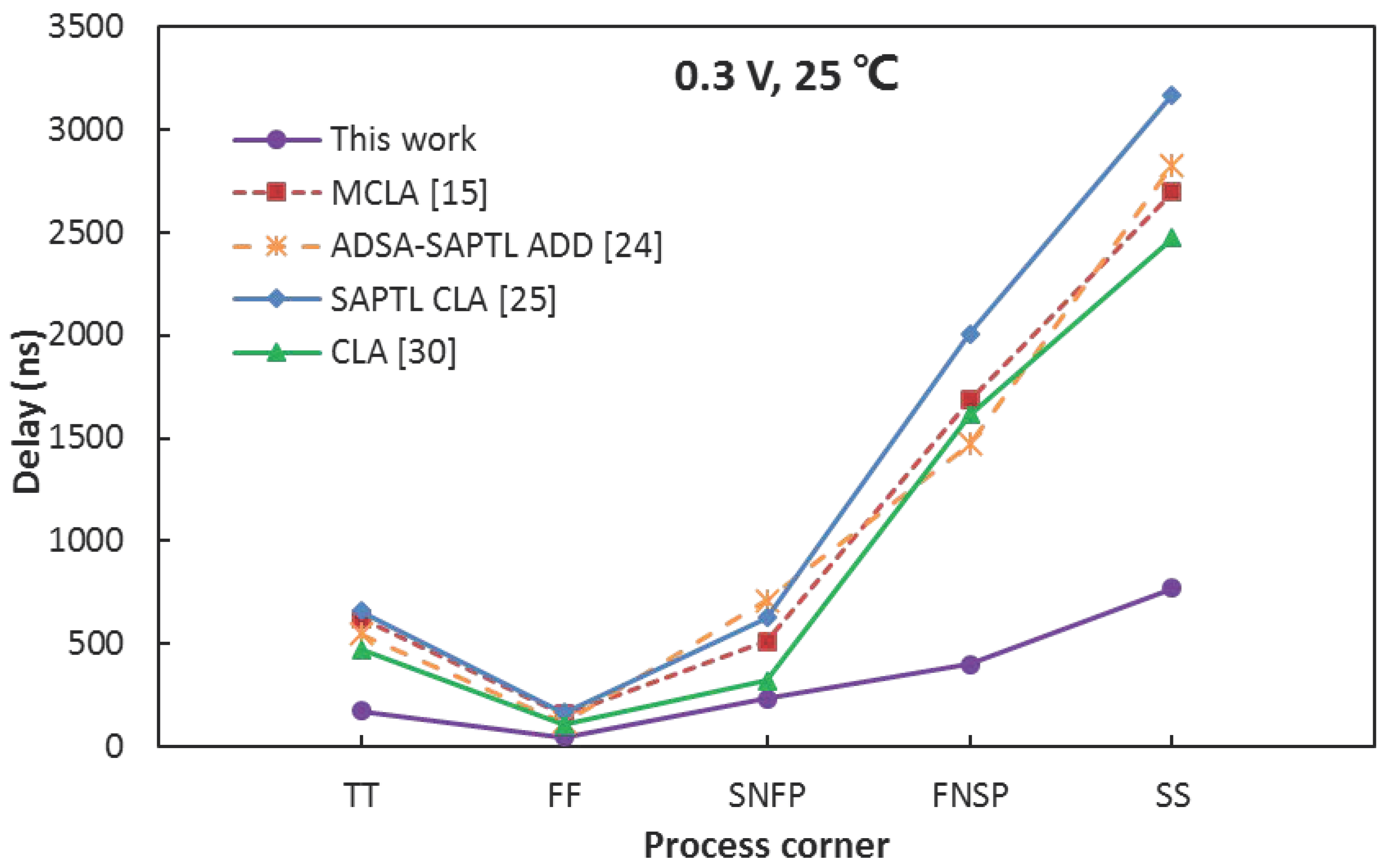
3.1. Comparison with Other Works

For comparison, a 16 bit modified CLA (MCLA) [15], a 16 bit adder based on asynchronous SAPTL (ADSA-SAPTL ADD) [24], a 16 bit SAPTL CLA [25], and a conventional 16 bit CLA [29] were also simulated using HSPICE in SMIC 130 nm technology. All these adders were sized based on the sizing scheme in Reference [29]. The V t h of SMIC 130 nm technology ranges from 365 mV to 450 mV with the channel width changing when L = 130 nm. Hence, we selected a V d d   = 0.3V to compare these 16 bit adders’ performance parameters, as presented in Table 2.
It can be observed that:
  • The proposed adder used 38% fewer transistors than ADSA-SAPTL ADD [24], 48% fewer than SAPTL CLA [25], and 35% fewer than the conventional CLA [30], which manifested the proposed architecture’s advantage on the area. But the proposed adder used more transistors than Reference [15], which meant extra area overhead.
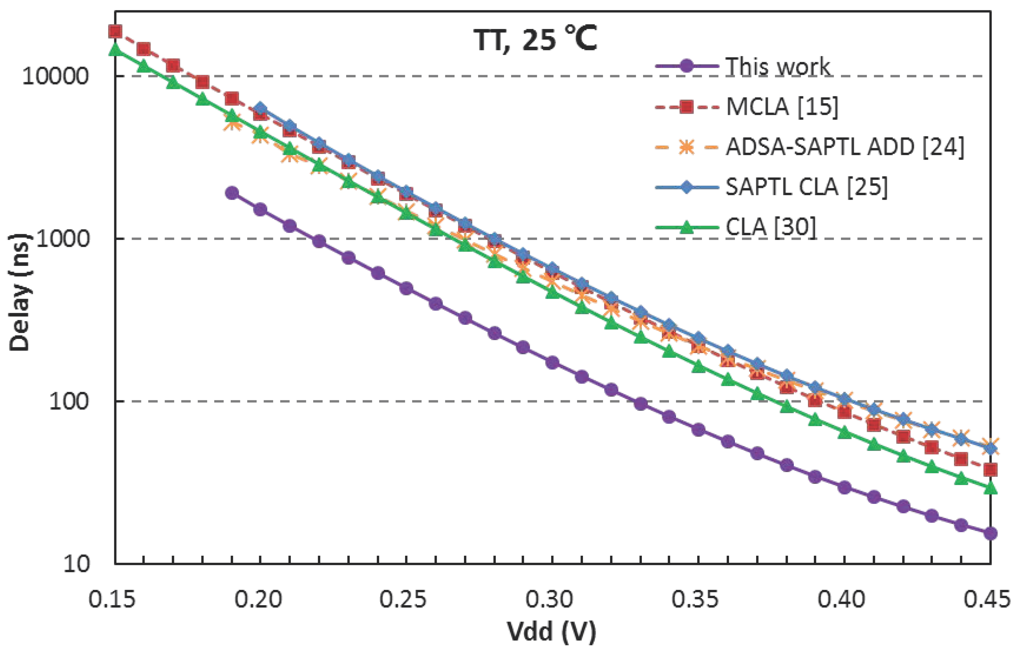
  • The bootstrapped SAPTL adder provided the best performance, 72% faster than the MCLA [15]. The maximum operating frequency of the proposed adder at 0.3 V (TT corner, 25 °C) achieved 5.5 MHz.
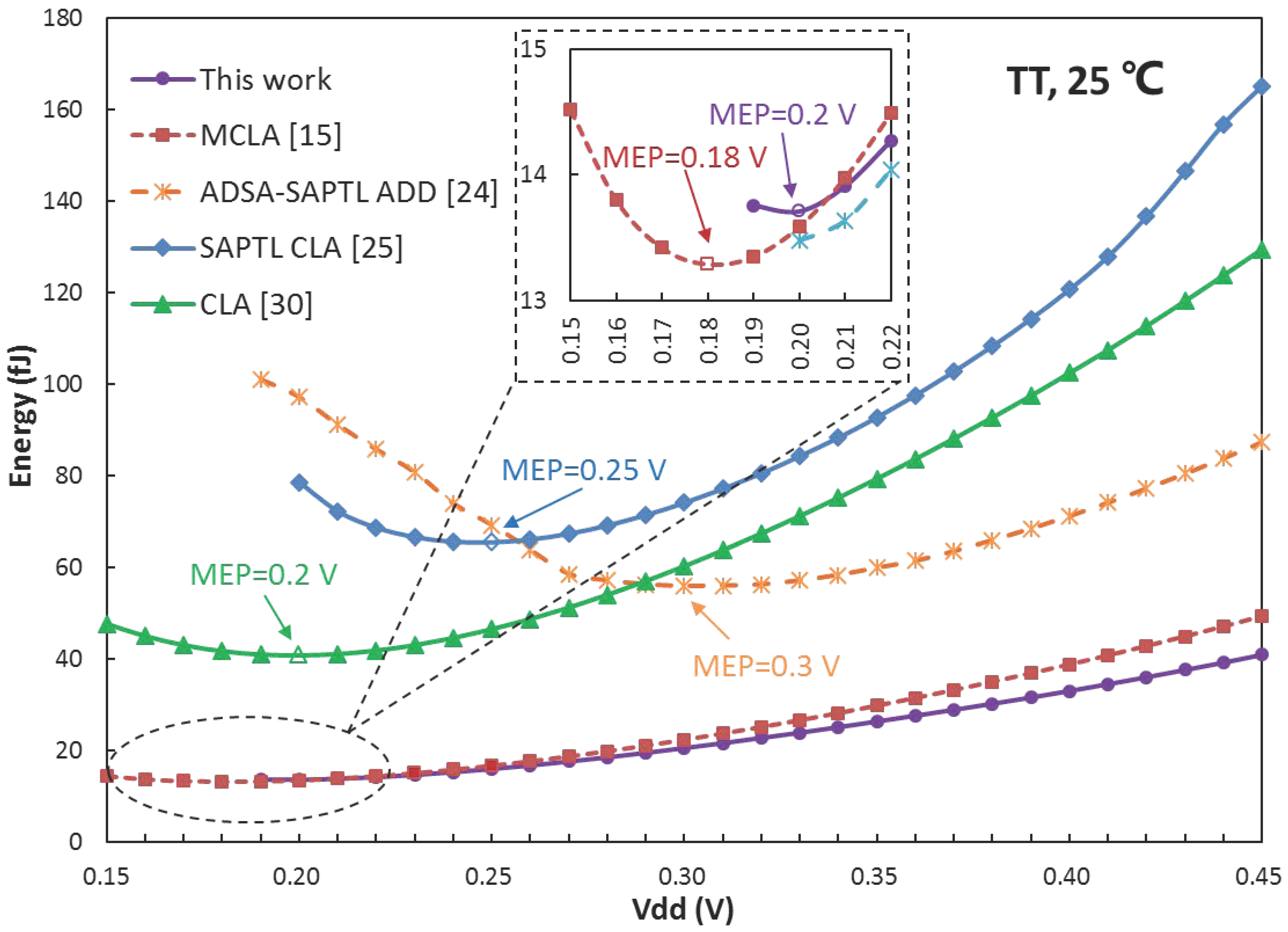
  • From the perspective of energy consumption, the bootstrapped SAPTL adder cost the lowest energy, 8.1% lower than the MCLA despite a larger area overhead.
  • As for energy efficiency, the proposed adder had a dominant advantage. The EDP of the bootstrapped SAPTL adder was 3.62 fJ/MHz, 74.1% lower than the MCLA [15], 88.2% lower than the ADSA-SAPTL ADD [24], 92.6% lower than the SAPTL CLA [25], and 87.4% lower than the conventional CLA [30].

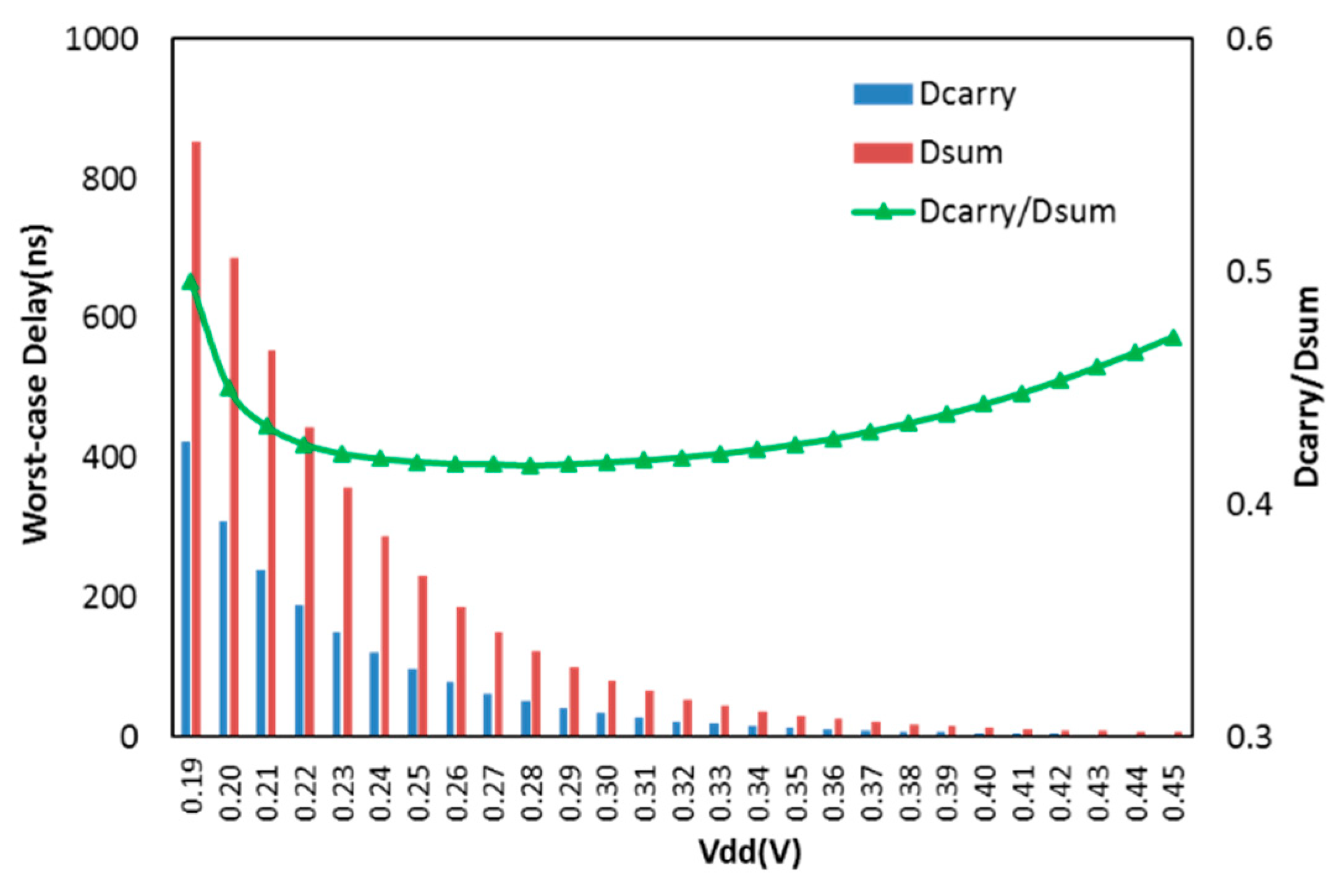
3.2. Worst-Case Delay versus Supply Voltage

Figure 8 plots the worst-case delays with supply voltage scaling in the subthreshold region. The minimum operating voltage of the bootstrapped SAPTL adder was 0.19 V.
As can be seen, the proposed adder had the fastest speed and its delay was one magnitude lower than other works in the subthreshold region. The enormous advantage over the other two SAPTL adders manifests the bootstrapped SA’s enhancement of speed.

3.3. Energy Consumption versus Supply Voltage

The energy consumptions for the worst case with supply voltage scaling are presented in Figure 9.
Owing to the fewer SAs used in the proposed adder architecture, the energy overhead of the bootstrapped SAPTL adder was far below the other two SAPTL adders. Furthermore, the proposed adder always consumed less energy than the MCLA when V d d 0.21   V . The minimum energy point (MEP) of the 16 bit bootstrapped SAPTL adder was 0.2 V. The corresponding minimum energy consumption was 13.71 fJ, 75.5% lower than ADSA-SAPTL’s 59.99 fJ at MEP = 0.3 V, 79.1% lower than SAPTL CLA’s 65.51 fJ at MEP = 0.25 V, and 66.5% lower than the conventional CLA’s 40.87 fJ at MEP = 0.2 V and was very close to MCLA’s 13.29 fJ at MEP = 0.18 V.

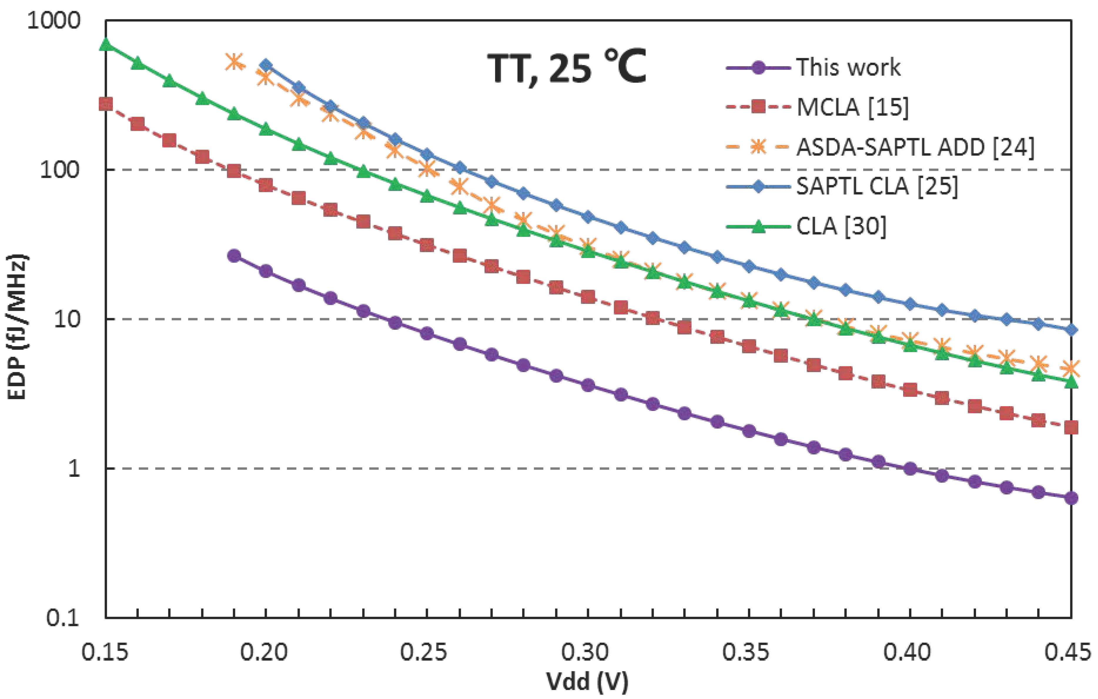
3.4. Energy-Delay Production versus Supply Voltage

The energy-delay production (EDP) is an important metric to evaluate the energy efficiency of a circuit [31]. Figure 10 shows the EDP of these 16 bit adders with supply voltage scaling.
It can be seen that the proposed adder had the lowest EDP in the subthreshold region, owing to better performance and lower energy overhead. The result implies that the proposed adder was the most energy-efficient among these adders.

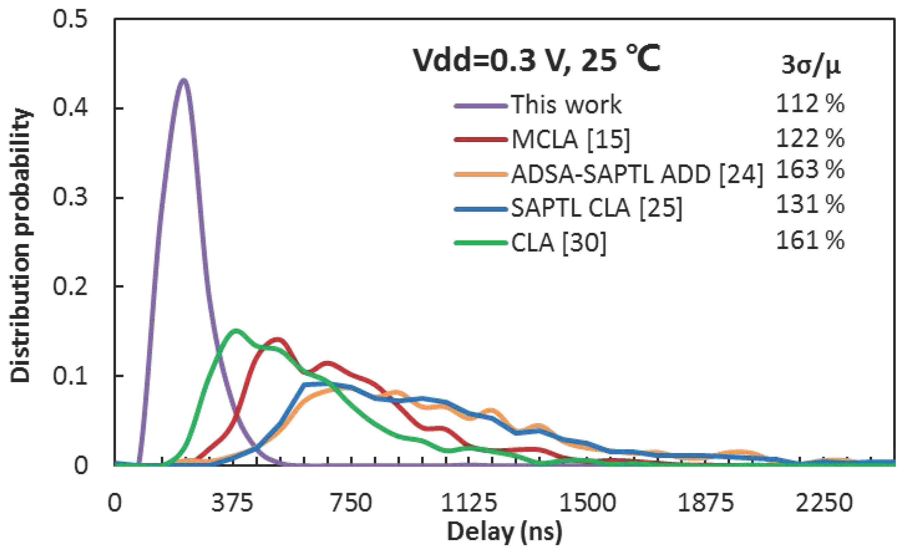
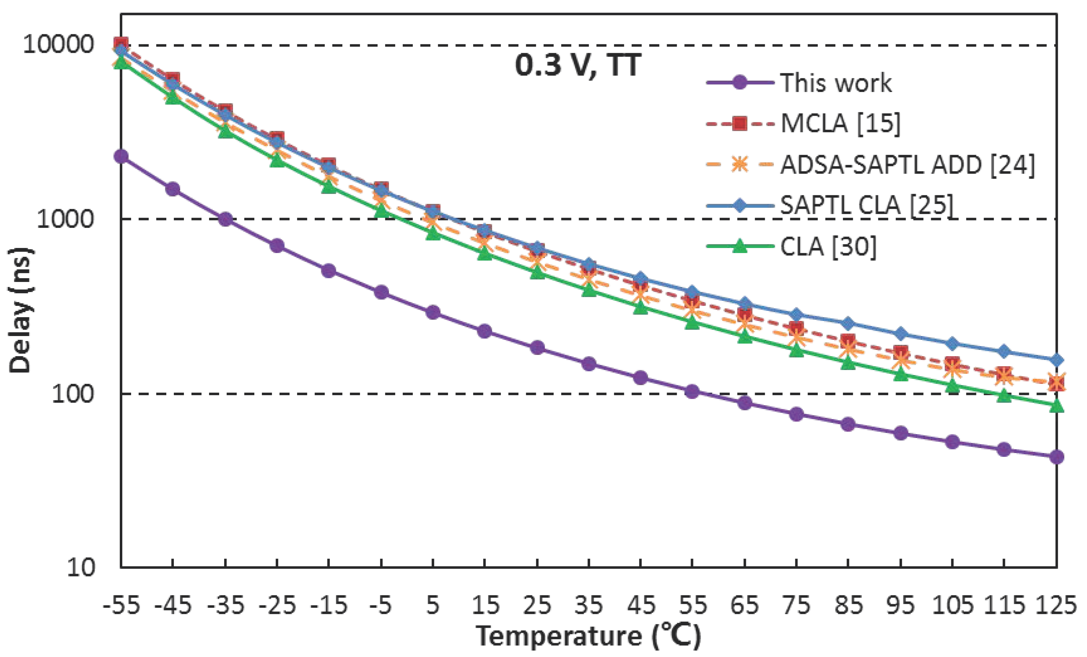
3.5. Simulation Results of Process and Temperature Variations

Through running 1000 times Monte Carlo simulations using HSPICE, the statistical distributions of the adders’ delays at 0.3 V were obtained and are shown in Figure 11. As can be seen from the graph, the distribution curve of the delay of the proposed 16 bit adder was obviously the most centralized with a relatively lowest ratio of standard deviation to average value (3σ/μ).
Moreover, Figure 12 presents the worst-case delay of different adders at all process corners. The results indicate that the proposed adder exhibited smaller performance fluctuations with the process corner varying.
Figure 13 depicts the changing curves of the delay with temperature variations. As can be seen, the proposed adder also had an evident advantage in the aspect of temperature sensibility.
Consequently, it can demonstrate that the proposed 16 bit adder had a lower sensitivity to process and temperature variations than the other adders.
On all accounts, the simulation results indicate that the proposed subthreshold adder based on a bootstrapped SAPTL circuit can improve performance effectively. Meanwhile, the energy consumption was reduced and, thus, the energy efficiency was improved significantly. The bootstrapped SAPTL adder also provided stronger immunity to process and temperature variations than other works.

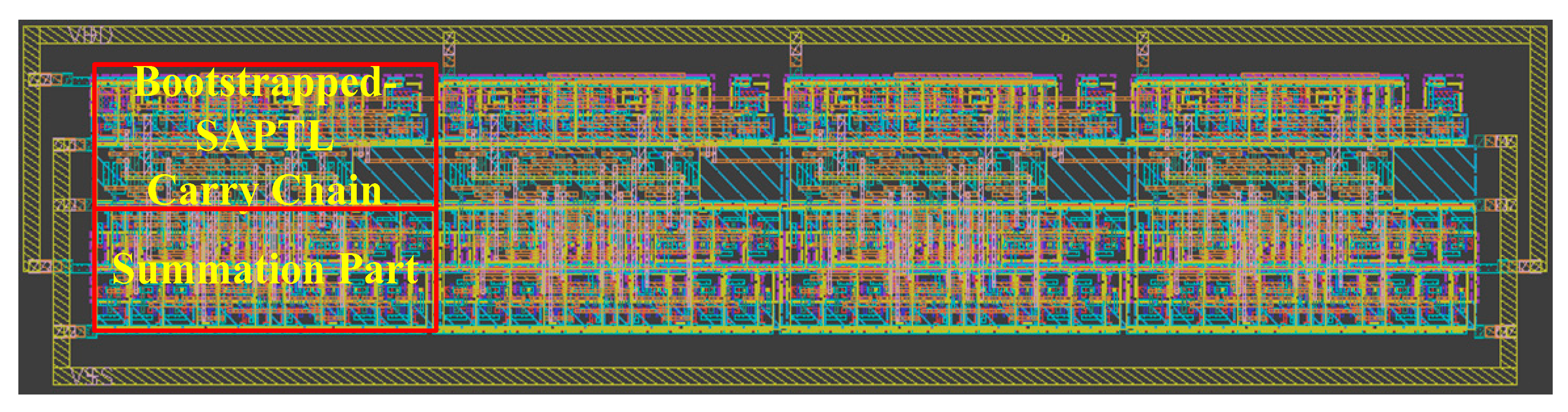
3.6. Post-Layout Simulation Result

Figure 14 shows the layout of the 16 bit bootstrapped SAPTL adder using SMIC 130 nm technology. The red pane is the carry chain part and the summation part of a 4 bit bootstrapped SAPTL adder block, respectively. The area was 95 μm × 21.5 μm. The worst-delay at 0.3 V (TT corner, 25 °C) obtained from the post-layout simulation was 230.17 ns and the energy consumption was 27.36 fJ. It is noticeable that the circuit’s performance was severely influenced due to the parasitic parameters in the subthreshold region. The layout still needs to be carefully optimized in future work.

4. Conclusions

In this paper, a subthreshold adder circuit which employed a bootstrapped sense amplifier in SAPTL and adopted a bootstrapped SAPTL-based architecture in the carry chain was proposed. The BSA enhanced the speed of the SAPTL effectively by enlarging the gate-source voltage. The proposed adder architecture was capable of exploiting the bootstrapped SAPTL’s advantage on performance in multi-bit adder circuits without using too many sense amplifiers. A 16 bit adder was studied in SMIC 130 nm technology. The comparison results demonstrated that the proposed 16 bit adder outperformed other works in terms of performance, energy consumption, energy efficiency, and the sensitivity to process and temperature variations in the subthreshold region. At 0.3 V, the proposed adder revealed a 72% less worst-case delay with 8% lower energy and 74% lower EDP as compared with an MCLA. However, there is still room for further optimization of the area and performance of the post-layout design. Furthermore, this work was only performed in SMIC 130 nm technology. It still needs to be applied to more advanced technology nodes to verify the advantages of the proposed design in future work.

Author Contributions

Conceptualization, Q.Z. and Y.W.; methodology, Q.Z.; validation, Q.Z. and Y.W.; formal analysis, Q.Z.; investigation, Q.Z.; resources, L.C.; data curation, Q.Z.; writing—original draft preparation, Q.Z.; writing–review and editing, Y.W. and L.C.; supervision, Y.W.; project administration, L.C.; funding acquisition, L.C.

Funding

This research was funded by the National Science and Technology Major Project grant number 2017ZX02301007-001 and the Beijing Science and Technology Special Project grant number Z171100001117147. The APC was funded by 2017ZX02301007-001.

Acknowledgments

Qi Zhang would like to thank Yuping Wu and Lan Chen, for their valuable advice and reviews of this paper, and the students and faculty of the EDA center of the Institute of Microelectronics of the Chinese Academy of Sciences for their support of this research.

Conflicts of Interest

The authors declare no conflict of interest.

References

  1. Lee, I.; Sylvester, D.; Blaauw, D. Subthreshold voltage reference with scalable output voltage for low-power IoT systems. IEEE J. Solid State Circuits 2017, 52, 1443–1449. [Google Scholar] [CrossRef]
  2. Sridhara, K.; Biradar, G.S.; Yanamshetti, R. Subthreshold leakage power reduction in VLSI circuits: A survey. In Proceedings of the International Conference on Communication and Signal Processing, Melmaruvathur, India, 6–8 April 2016; pp. 1120–1124. [Google Scholar] [CrossRef]
  3. Dokic, B.; Pajkanovic, A. Low power CMOS sub-threshold circuits. In Proceedings of the 36th International Convention on Information and Communication Technology, Electronics and Microelectronics (MIPRO), Opatija, Croatia, 20–24 May 2013; pp. 60–65. [Google Scholar] [CrossRef]
  4. Wang, A.; Chandrakasan, A. A 180-mV subthreshold FFT processor using a minimum energy design methodology. IEEE J. Solid State Circuits 2005, 40, 310–319. [Google Scholar] [CrossRef]
  5. Verma, N.; Kwong, J.; Chandrakasan, A.P. Nanometer MOSFET variation in minimum energy subthreshold circuits. IEEE Trans. Electron. Devices 2008, 55, 163–174. [Google Scholar] [CrossRef]
  6. Keane, J.; Eom, H.; Kim, T.H.; Sapatnekar, S.; Kim, C. Stack sizing for optimal current drivability in subthreshold circuits. IEEE Trans. Very Large Scale Integr. VLSI Syst. 2008, 16, 598–602. [Google Scholar] [CrossRef]
  7. Hanson, S.; Zhai, B.; Seok, M.; Cline, B.; Zhou, K.; Singhal, M.; Minuth, M.; Olson, J.; Nazhandali, L.; Austin, T. Exploring variability and performance in a sub-200-mV processor. IEEE J. Solid State Circuits 2008, 43, 881–891. [Google Scholar] [CrossRef]
  8. Calhoun, B.H.; Chandrakasan, A.P. Ultra-dynamic voltage scaling (UDVS) using sub-threshold operation and local voltage dithering. IEEE J. Solid State Circuits 2006, 41, 238–245. [Google Scholar] [CrossRef]
  9. Bo, Z.; Hanson, S.; Blaauw, D.; Sylvester, D. Analysis and mitigation of variability in subthreshold design. In Proceedings of the 2005 International Symposium on Low Power Electronics and Design, San Diego, CA, USA, 8–10 August 2005; pp. 20–25. [Google Scholar] [CrossRef]
  10. Dorosti, H.; Teymouri, A.; Fakhraie, S.M.; Salehi, M. Ultralow-Energy Variation-Aware Design: Adder Architecture Study. IEEE Trans. Very Large Scale Integr. VLSI Syst. 2016, 24, 1165–1168. [Google Scholar] [CrossRef]
  11. Pradhan, S.N.; Rai, V.; Chakraborty, A. Design of high speed and low power full adder in subthreshold region. In Proceedings of the 2016 International Conference on Microelectronics, Computing and Communications (MicroCom), Durgapur, India, 23–25 January 2016; pp. 1–6. [Google Scholar] [CrossRef]
  12. Jafari, M.; Imani, M.; Ansari, M.; Fathipour, M.; Sehatbakhsh, N. Design of an ultra-low power 32-bit adder operating at subthreshold voltages in 45-nm FinFET. In Proceedings of the International Conference on Design & Technology of Integrated Systems in Nanoscale Era, Abu Dhabi, UAE, 26–28 March 2013; pp. 167–168. [Google Scholar] [CrossRef]
  13. Attarzadeh, H.; Aunet, S.; Ytterdal, T. An ultra-low-power/high-speed 9-bit adder design: Analysis and comparison Vs. technology from 130nm-LP to UTBB FD-SOI-28nm. In Proceedings of the 2015 Nordic Circuits and Systems Conference (NORCSA), Oslo, Norway, 26–28 October 2015; pp. 1–4. [Google Scholar] [CrossRef]
  14. Granhaug, K.; Aunet, S. Six Subthreshold Full Adder Cells characterized in 90 nm CMOS technology. In Proceedings of the 2016 IEEE Design and Diagnostics of Electronic Circuits and Systems, Prague, Czech Republic, 18–21 April 2006; pp. 25–30. [Google Scholar] [CrossRef]
  15. Ghobadi, N.; Majidi, R.; Mehran, M.; Afzali-Kusha, A. Low Power 4-Bit Full Adder Cells in Subthreshold Regime. In Proceedings of the 18th Iranian Conference on Electrical Engineering, Isfahan, Iran, 11–13 May 2010; pp. 362–367. [Google Scholar] [CrossRef]
  16. Pakniyat, E.; Talebiyan, S.R.; Morad, M.J.A. Design of High performance and Low Power 16T Full Adder Cell for Sub-threshold Technology. In Proceedings of the 2015 International Conference on Technology, Communication and Knowledge (ICTCK), Mashhad, Iran, 11–12 November 2015; pp. 79–85. [Google Scholar] [CrossRef]
  17. Tamang, D.; Pandey, V.; Singh, N.K. A Sub-Threshold Operation of XOR based Energy Efficient Full Adder. In Proceedings of the 2016 International Conference on Communication and Signal Processing (ICCSP), Melmaruvathur, India, 6–8 April 2016; pp. 1066–1069. [Google Scholar] [CrossRef]
  18. Monteiro, J.; Guntzel, J.L.; Agostini, L. A1CSA: An energy-efficient fast adder architecture for cell-based VLSI design. In Proceedings of the 18th IEEE International Conference on Electronics, Circuits, and Systems, Beirut, Lebanon, 11–14 December 2011; pp. 442–445. [Google Scholar] [CrossRef]
  19. Tran, A.T.; Baas, B.M. Design of an energy-efficient 32-bit adder operating at subthreshold voltages in 45-nm CMOS. In Proceedings of the International Conference on Communications and Electronics, Nha Trang, Vietnam, 11–13 August 2010; pp. 87–91. [Google Scholar] [CrossRef]
  20. Gupta, P.; Munje, I.; Kaswan, N.; Asati, A.; Gupta, A. Analysis & Implementation of Ultra Low Power 4-bit CLA in Subthreshold Regime. In Proceedings of the 2014 International Conference on Circuits, Power and Computing Technologies (ICCPCT), Nagercoil, India, 20–21 March 2014; pp. 1074–1076. [Google Scholar] [CrossRef]
  21. Alarcón, L.P.; Liu, T.T.; Pierson, M.D.; Rabaey, J.M. Exploring very low-energy logic: A case study. J. Low Power Electron. 2007, 3, 223–233. [Google Scholar] [CrossRef]
  22. Markovic, D.; Wang, C.C.; Alarcón, L.P.; Liu, T.T.; Rabaey, J.M. Ultralow-power design in near-threshold region. Proc. IEEE 2010, 98, 237–252. [Google Scholar] [CrossRef]
  23. Ho, W.G.; Chong, K.S.; Gwee, B.H.; Chang, J.S.; Sun, Y.; Chang, K.L. Improved Asynchronous-Logic Dual-Rail Sense Amplifier-Based Pass Transistor Logic with High Speed and Low Power Operation. In Proceedings of the 2011 IEEE International Symposium of Circuits and Systems (ISCAS), Rio de Janeiro, Brazil, 15–18 May 2011; pp. 1936–1939. [Google Scholar] [CrossRef]
  24. Zhang, Q.; Wu, Y.; Chen, L.; Zhang, X.; Shi, W. SAPTL–based Robust Sub-threshold Adder Circuit Design. In Proceedings of the 13th IEEE International Conference on Solid-State and Integrated Circuit Technology (ICSICT), Hangzhou, China, 25–28 October 2016; pp. 1–3. [Google Scholar] [CrossRef]
  25. Dang, F.; Wang, Y.; Liu, Y.; Jia, S.; Zhang, X. Design on Multi-bit Adder Using Sense Amplifier-Based Pass Transistor Logic for Near-Threshold Voltage Operation. In Proceedings of the 2015 IEEE 11th International Conference on ASIC (ASICON), Chengdu, China, 3–6 November 2015; pp. 1–4. [Google Scholar] [CrossRef]
  26. Alarcón, L.P.; Liu, T.T.; Rabaey, J.M. A low-leakage parallel CRC generator for ultra-low power applications. In Proceedings of the 2011 IEEE International Symposium of Circuits and Systems (ISCAS), Rio de Janeiro, Brazil, 15–18 May 2011; pp. 2063–2066. [Google Scholar] [CrossRef]
  27. Alarcón, L.P. Sense Amplifier-based Pass Transistor Logic. Ph.D. Thesis, University of California at Berkeley, Berkeley, CA, USA, 2010. [Google Scholar]
  28. Kao, J.T.; Chandrakasan, A.P. Dual-threshold voltage techniques for low-power digital circuits. IEEE J. Solid State Circuits 2000, 35, 1009–1018. [Google Scholar] [CrossRef]
  29. Nabavi, M.; Ramezankhani, F.; Shams, M. Optimum pMOS-to-nMOS Width Ratio for Efficient Subthreshold CMOS Circuits. IEEE Trans. Electron. Devices 2016, 63, 916–924. [Google Scholar] [CrossRef]
  30. Weste, N.; Harris, D. CMOS VLSI Design: A Circuits and Systems Perspective, 4th ed.; Addison-Wesley: Boston, MA, USA, 2011; pp. 443–468. [Google Scholar]
  31. Wang, A.; Calhoun, B.H.; Chandrakasan, A.P. Minimizing Energy Consumption. In Sub-Threshold Design for Ultra Low-Power Systems; Chandrakasan, A.P., Ed.; Springer: Boston, MA, USA, 2006; pp. 42–48. [Google Scholar]
Figure 1. The structure of the bootstrapped sense amplifier.
Electronics 08 01161 g001
Figure 2. The simulated waveform of the BSA circuit.
Electronics 08 01161 g002
Figure 3. The 4 bit bootstrapped sense amplifier-based pass transistor logic (SAPTL) adder block.
Electronics 08 01161 g003
Figure 4. The pass transistor network (PTN) structure of the carry chain of the 4 bit adder block.
Electronics 08 01161 g004
Figure 5. The timing diagram of the bootstrapped SAPTL.
Electronics 08 01161 g005
Figure 6. D c a r r y and D s u m versus V d d .
Electronics 08 01161 g006
Figure 7. The proposed 16 bit adder: (a) block diagram; (b) transient simulated waveform.
Electronics 08 01161 g007
Figure 8. The worst-case delay versus V d d .
Electronics 08 01161 g008
Figure 9. The energy consumption per operation versus V d d .
Electronics 08 01161 g009
Figure 10. The energy-delay production (EDP) versus V d d .
Electronics 08 01161 g010
Figure 11. The statistical distributions of the delay at 0.3 V.
Electronics 08 01161 g011
Figure 12. The worst-case delays at all process corners at 0.3 V.
Electronics 08 01161 g012
Figure 13. The performance variety with temperature.
Electronics 08 01161 g013
Figure 14. The layout of the proposed 16 bit adder.
Electronics 08 01161 g014
Table 1. The sizing of different parts in the proposed adder circuit.
Circuit ModuleWidth/Length of PMOSWidth/Length of NMOSFingers
Stack driver (plvt)750 nm/130 nm150 nm/130 nm1
PTN (nlvt)-150 nm/130 nm1
PMOS capacitor in BSA1.1 μm/1.1 μm-1
INV in BSA560 nm/130 nm150 nm/130 nm1
NOR in BSA300 nm/130 nm150 nm/130 nm1
Other transistors in BSA150 nm/130 nm150 nm/130 nm1
FA900 nm/130 nm150 nm/130 nm1
XOR600 nm/130 nm150 nm/130 nm1
plvt: low-threshold PMOS transistors; nlvt: low-threshold NMOS transistors; BSA: bootstrapped sense amplifier.
Table 2. Comparison with other works at 0.3 V (TT corner, 25 °C).
Reference[15][24][25][30]This work
Transistor number420 ()1056 (2.51×)1260 (3.00×)1000 (2.38×)648 + 4 MOS-caps (1.55×)
Worst-case delay (ns)623.62 ()547.25 (0.88×)658.19 (1.06×)474.01 (0.76×)175.48 (0.28×)
Energy (fJ)22.45 ()55.99 (2.49×)74.15 (3.30×)60.37 (2.69×)20.63 (0.92×)
Energy-delay production (fJ/MHz)14.00 ()30.64 (2.19×)48.81 (3.49×)28.62 (2.04×)3.62 (0.26×)
The bold-faced numbers in the round brackets represent the normalized ratio.

