2. Proposed Circuit Technique to Relax the Feedback Timing of the Input Feed-Forward ΔΣ ADC
One of the main delay sources in the feedback path of the low-distortion ΔΣ ADC is a DEM to shape the DAC mismatch error.
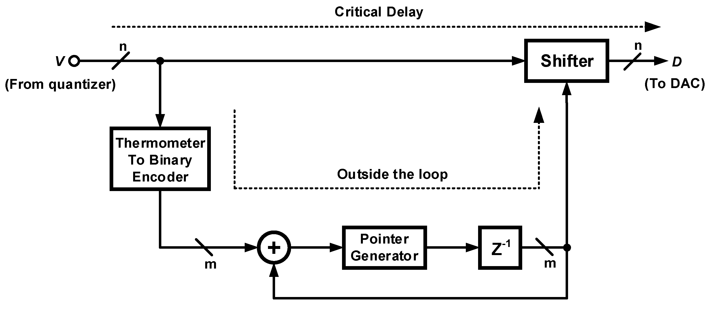
Figure 1 shows a conventional DEM block diagram. It consists of a thermometer to binary encoder, pointer generator, and shifter. The pointer indicates which unit element should be used as the starting point in the DAC operation. The shifter maps the relationship between the thermometer code from the quantizer and DAC unit elements. As shown in
Figure 1, because the operation of the encoder and pointer generator should be undertaken outside the feedback loop, the total feedback delay does not consider their delays. However, the total amount of feedback delay directly depends on the shifter delay since it is inside the ADC loop. Therefore, the shifter delay is an important factor used to estimate the feedback delay of the modulator.
There are two types of shifters: A barrel shifter and a logarithmic shifter [
4]. Each shifter has a trade-off between power consumption and propagation delay. The propagation delay of the barrel shifter is constant and independent of the shifter value or size because input data transfers to the output passing through only one gate. Therefore, it is useful for high-speed operation. However, the barrel shifter will consume more power than the logarithmic shifter due to the decoder. By contrast, the propagation delay of the logarithmic shifter is large and depends on the number of stages because the input data should pass through every stage. In other words, the logarithmic shifter is appropriate for low-speed operation with less power consumption.
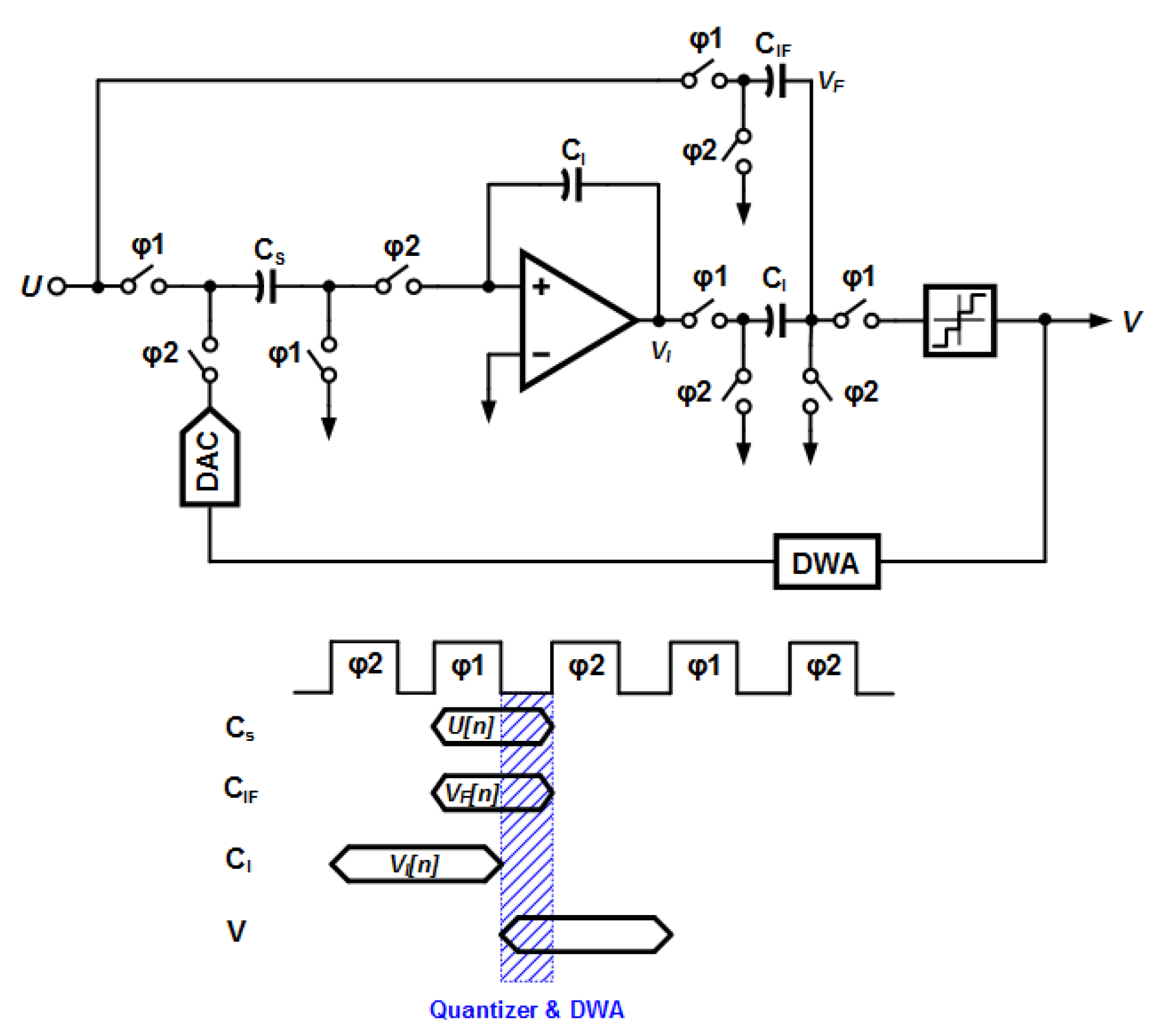
Figure 2 shows the simplified first-order, single-ended switched capacitor circuit and timing diagram of the traditional input feed-forward topology [
5]. A quantizer requires V
F[n] and V
I[n] to generate digital output V. Then, digital output needs to be fed back to the input before φ2 for DAC operation. Because V
F[n] appears at the end of φ1, only non-overlapping time between φ1 and φ2 is available to operate the quantizer and DEM. Therefore, a fast quantizer and DEM logic are needed to satisfy the stringent timing requirement of the high-speed modulator. This results in increasing total power dissipation in the conventional low-distortion architecture. The easiest and simplest method which can be used to relax the feedback timing is to extend the non-overlapping time for the quantizer and DEM logic. However, this will reduce the available integration time of each integrator, which can cause slewing or distortion problems. Also, more power should be dissipated to meet the required settling error.
Manifold circuit techniques and topologies have been proposed to try and relax the stringent feedback timing of a low-distortion ΔΣ ADC [
5,
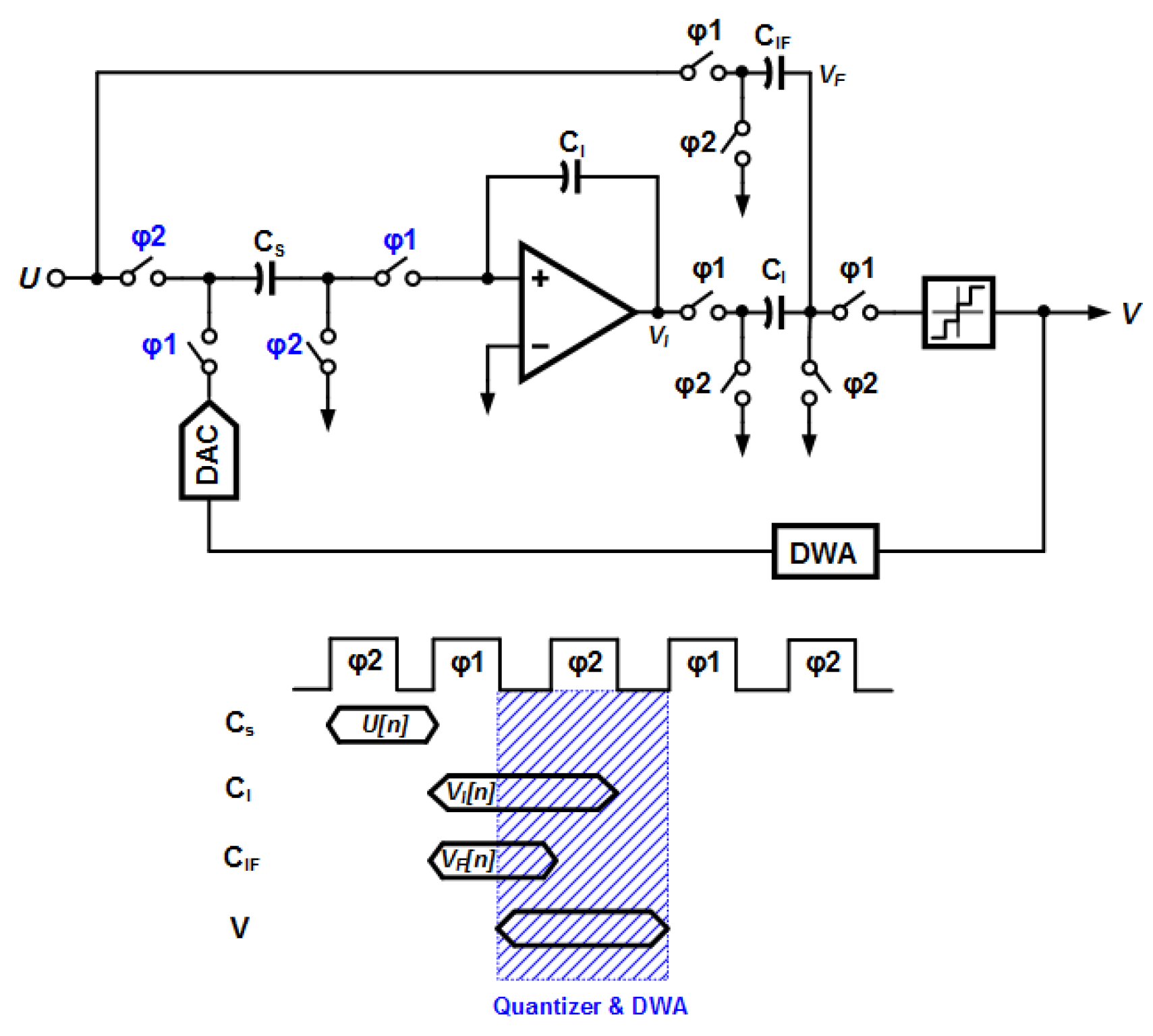
6]. However, these kinds of techniques require additional complicated circuitry, as well as more power dissipation. The SC circuit and its timing diagram applying a simple circuit technique to alleviate feedback timing is shown in
Figure 3.
Similarly, a quantizer still requires V
F[n] and V
I[n] to create the modulator output V. Also, V
F[n] is available at the end of φ1, as before, and shown in
Figure 2. However, by inserting simple delay elements in the feedback path and changing the sampling phase (φ1) and integration phase (φ2) at the input branch, the available feedback time increases by the amount of one full clock cycle. In other words, the sum of one full clock cycle and non-overlapping time is available for the quantizer and DEM operation. As a result, the digital output can be fed back to be input into the next φ1 phase instead of the φ2 phase. Therefore, a low-speed comparator and logarithmic shifter can be implemented even for high-speed applications. This will improve the performance of the ΔΣ modulator in terms of total power consumption.
3. Circuit Implementation
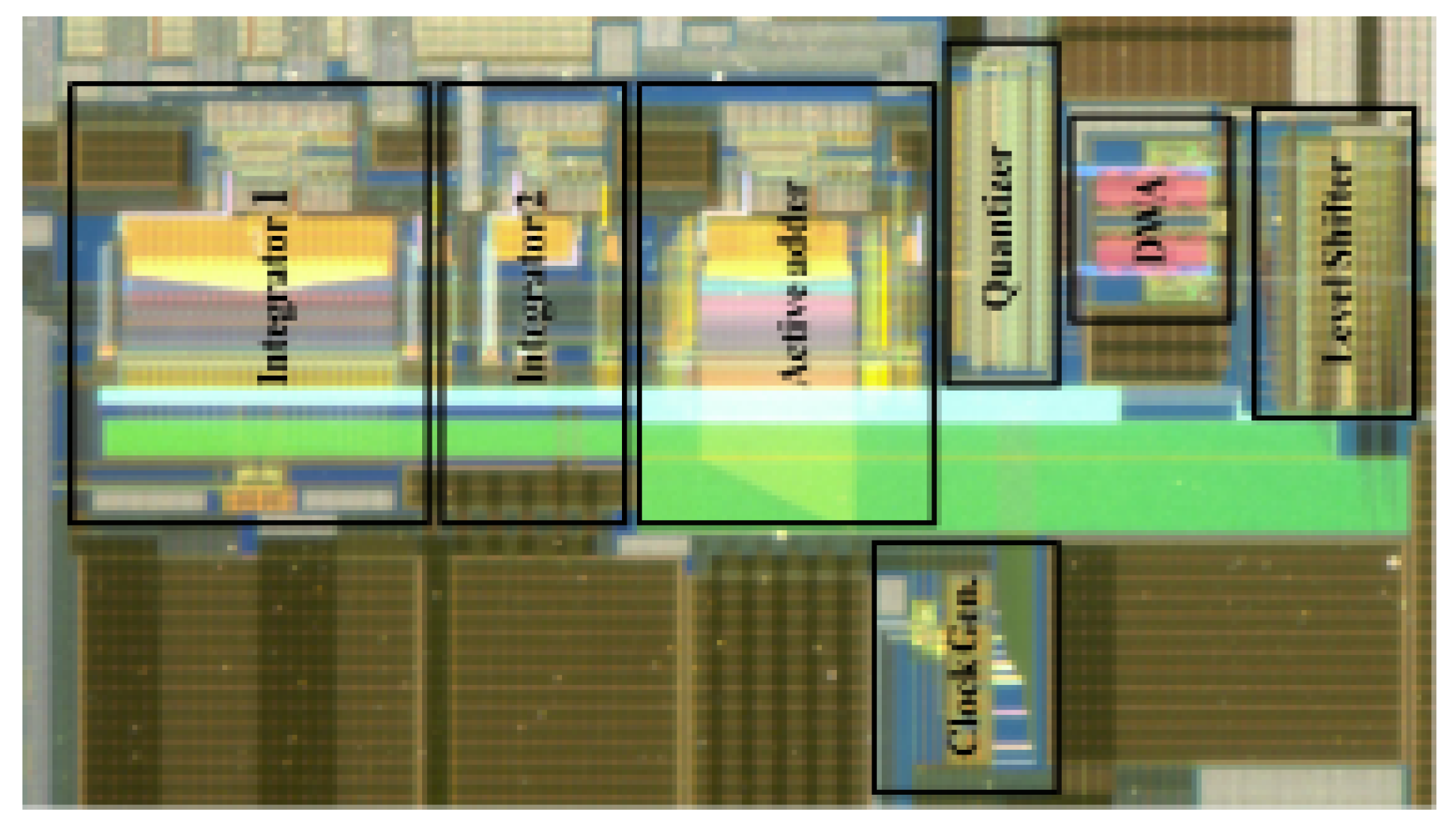
The ΔΣ modulator with the proposed circuit technique was implemented in a 0.18 um 2-poly and 4-metal CMOS process.
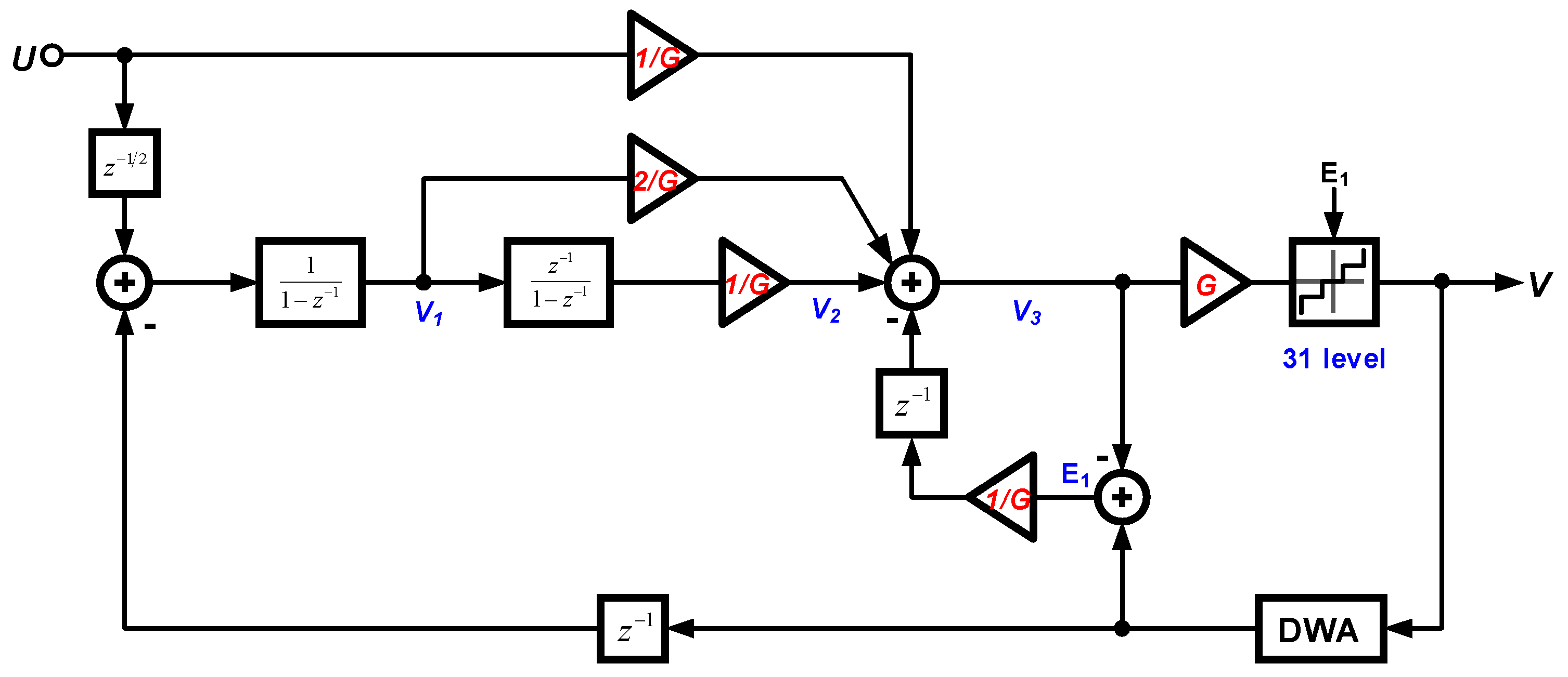
Figure 4 shows the improved ΔΣ modulator using relaxed feedback timing and a gain scaling technique.
In this block diagram, changes in the sampling phase and integration phase are represented by z
−1/2. Quantization noise was also extracted, delayed, and subtracted at the summing node before the quantizer. The injected, shaped quantization noise effectively increased the order of noise shaping by one without adding active components [
7]. Therefore, only three integrators are needed to achieve third-order noise shaping using the noise coupling technique, while four integrators are required in a conventional ΔΣ modulator. Also, we were able to use a low-power consuming logarithmic shifter and low-speed comparator with the aid of relaxed feedback timing. One drawback of this topology is that it necessitates an analog adder to sum signals from each integrator, including a large input signal. Therefore, the feedback factor of the adder is lowered, and the output swing is large due to its large input signal. This can cause slewing, non-linear distortion, and larger power consumption. To overcome these problems, a gain scaling technique was used in the modulator, as shown in
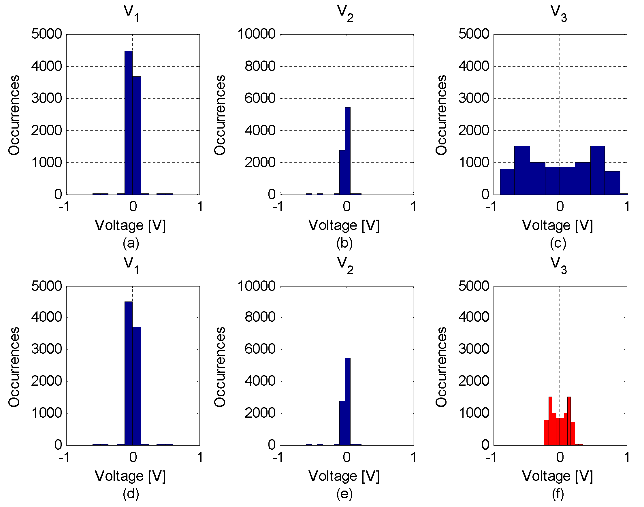
Figure 4. With this technique, the swing magnitude of the adder can be significantly reduced, and the feedback factor increased. As shown in the histogram in
Figure 5 with G = 4, the swing amplitude of the active adder, V
3, is decreased greatly compared to a configuration without gain scaling, enabling the adder to reduce power dissipation. Output swings of the rest of the integrators are the same even with the application of the gain scaling technique, as shown in
Figure 5.
This technique needs a gain of G in front of the quantizer to compensate for the reduced gain, as shown in
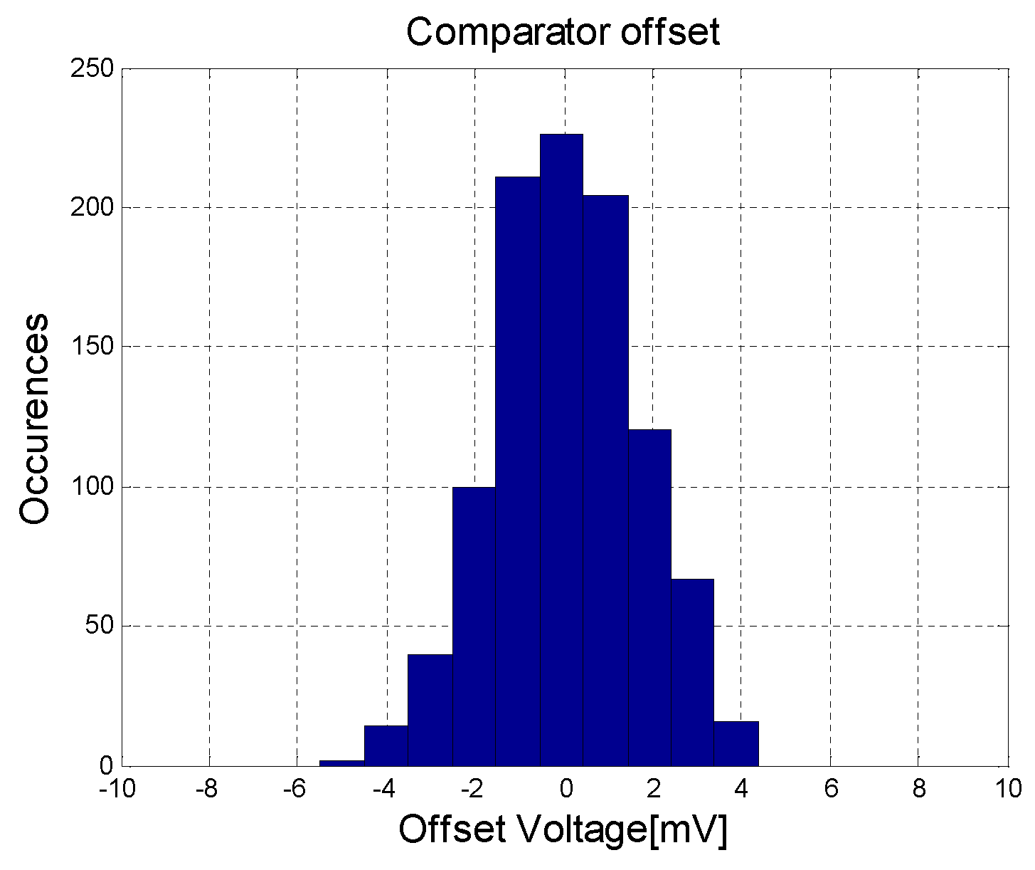
Figure 4. The gain can be easily realized by reducing the reference voltage of the internal quantizer by a factor of G. In this implementation, the positive reference, VRP is 2.65 V, negative VRN is 0.65 V, and output common mode voltage is 1.65 V. However, the positive reference for quantizer VRPQ is 1.9 V, and the negative reference for quantizer VRNQ is 1.4 V to generate an effective gain of 4. With the reduced quantizer reference, the quantizer needs to be more immune to offset voltage. The Monte-Carlo simulation was carried out 1000 times in Hspice based on the designed comparator with a three-sigma threshold voltage variation for all transistors.
Figure 6 shows the simulation result with a maximum offset voltage of 5 mV, which is less than half of 1 LSB.
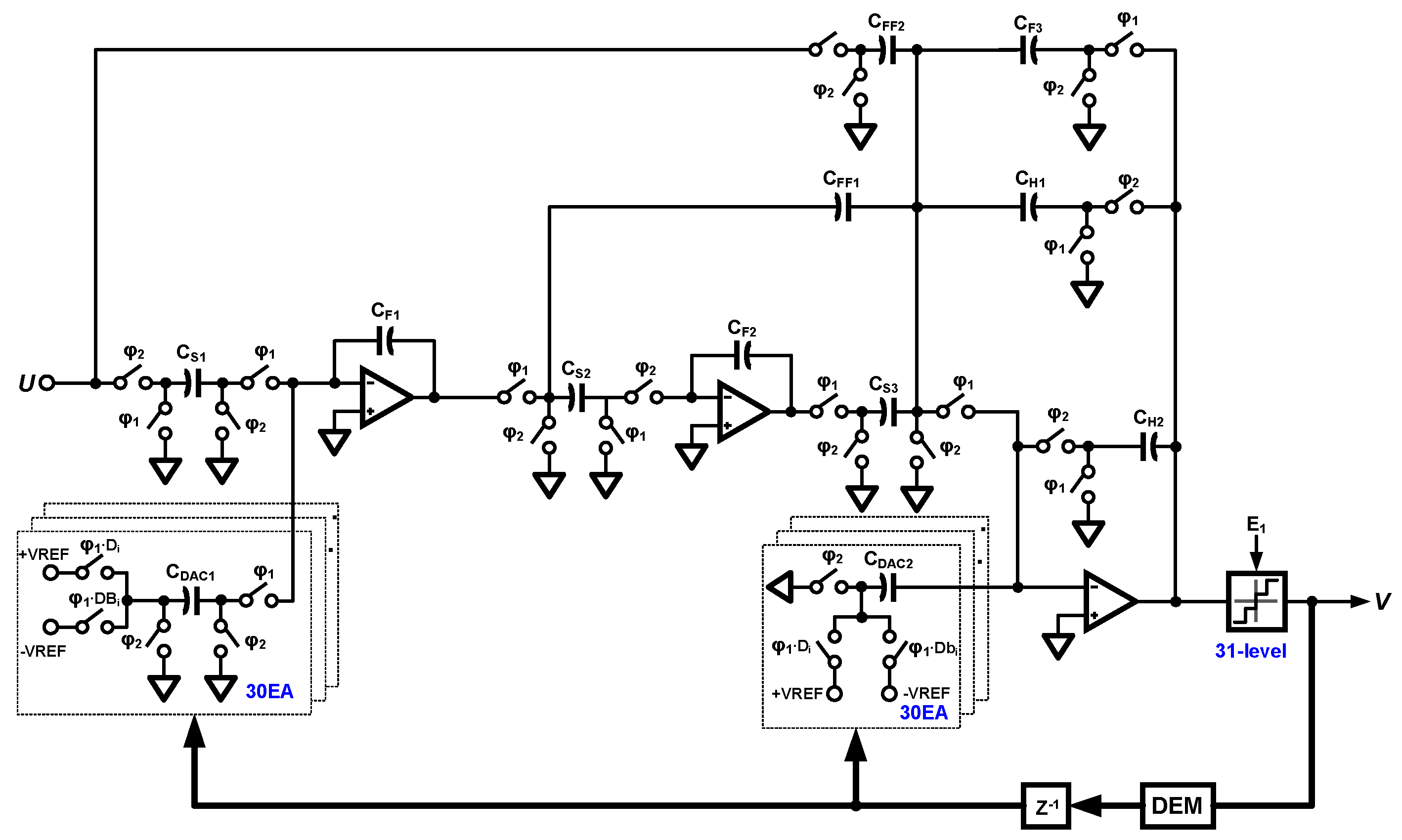
Figure 7 shows the simplified switched capacitor circuit diagram. The sampling and DAC capacitors at the input of the modulator have been separated to avoid signal-dependent loading on the references of the DACs [
8]. A poly-insulator-ploy (PIP) capacitor was used instead of a metal-insulator-metal (MIM) one to achieve better matching performance, even though the PIP capacitor has more parasitic capacitance based on the design manual. A bootstrapped switch was used to sample the input signal to guarantee linearity over a wide signal range and prevent signal-dependent charge injection [
9]. One full clock cycle delay (z
−1) from digital output to input DACs was realized by simple D flip-flops.
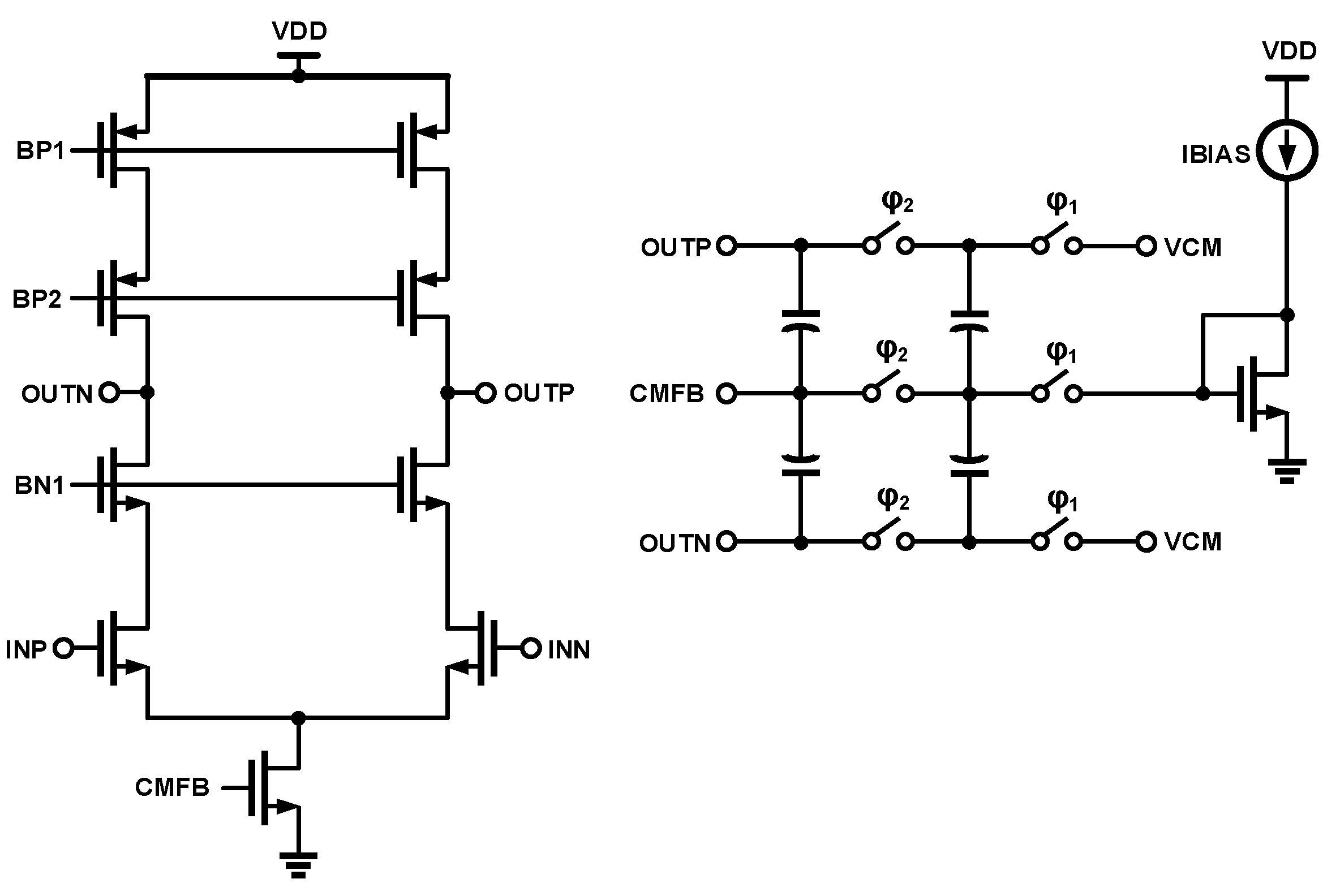
A power-efficient telescopic amplifier with switched-capacitor common-mode feedback was designed for two integrators and the active adder with 3.3 V power supply, as shown in
Figure 8. Input referred noise from the top PMOS was minimized by assigning a small trans-conductance. Also, the input pairs of the amplifier used NMOS to maximize energy efficiency [
7]. The proposed circuit technique to relax the feedback timing allowed for use of a low-speed shifter for low power consumption. Therefore, DEM logic with a logarithmic shifter was implemented to linearize the mismatch of the 30-level DAC [
10]. Two sets of DEM were implemented to relax the circuit design complexity, as illustrated in
Figure 9. DEM circuitry operates with a 1.5 V power supply, and their outputs are shifted by a level-up shifter to 3.3 V for proper DAC operation.
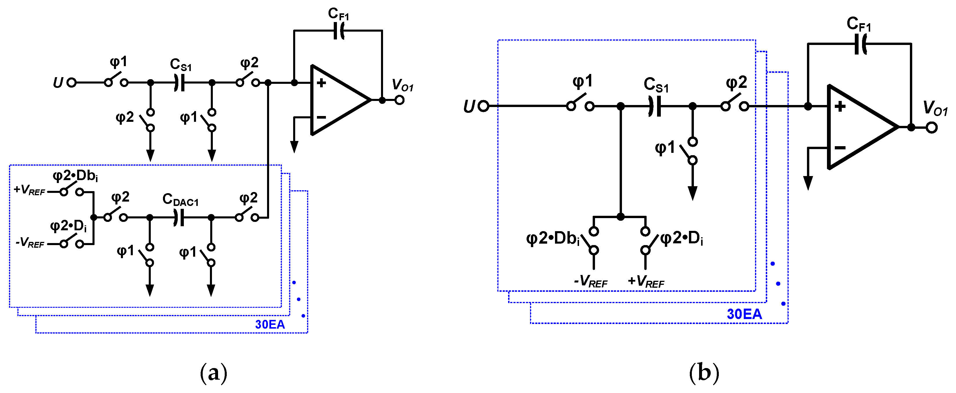
In this implementation, two slightly different prototypes were fabricated. They differed only in their input branches, as shown in
Figure 10. In prototype A, the sampling capacitor is separated from the DAC capacitor, while they are shared in prototype B. Theoretically, prototype B has half the kT/C noise of prototype A due to less input capacitance at the input branch of the modulator.
5. Conclusion
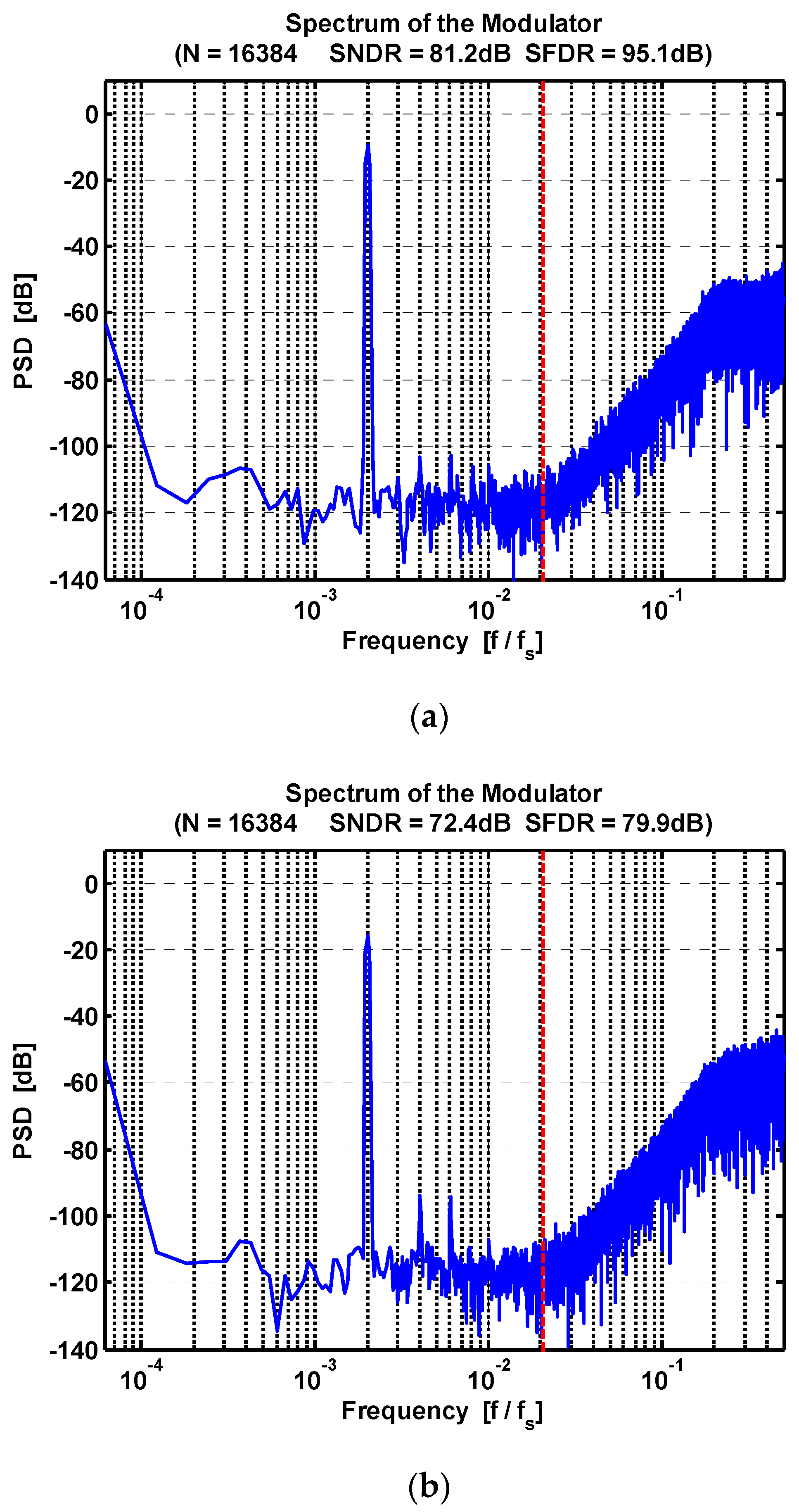
In this paper, a timing-relaxed, low-distortion ΔΣ modulator using a simple circuit technique was proposed for wideband and high-accuracy applications. Two improved prototypes using relaxed feedback timing and a gain scaling technique were fabricated with a 0.18 um 2P4M CMOS process. In prototype A, the sampling capacitor was separated from DAC capacitors, while they were shared in prototype B. Prototype A achieved a 90.5 dB dynamic range, 81.2 dB SNDR, and 95.1 dB SFDR, while prototype B achieved a 95.6 dB dynamic range, 72.4 dB SNDR, and 80 dB SFDR up to 2.1 MHz with the same testing environment. The total power consumption was 98 mW with a power supply (analog 3.3 V, digital 1.5 V).


