A 103 dB DR Fourth-Order Delta-Sigma Modulator for Sensor Applications


Abstract
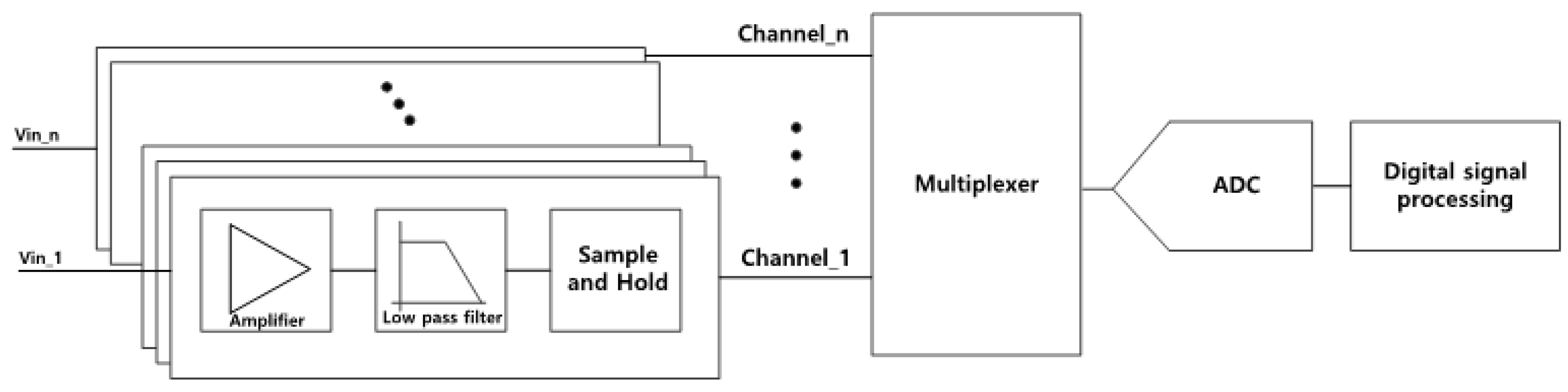
1. Introduction
2. Circuit Design and Implementation
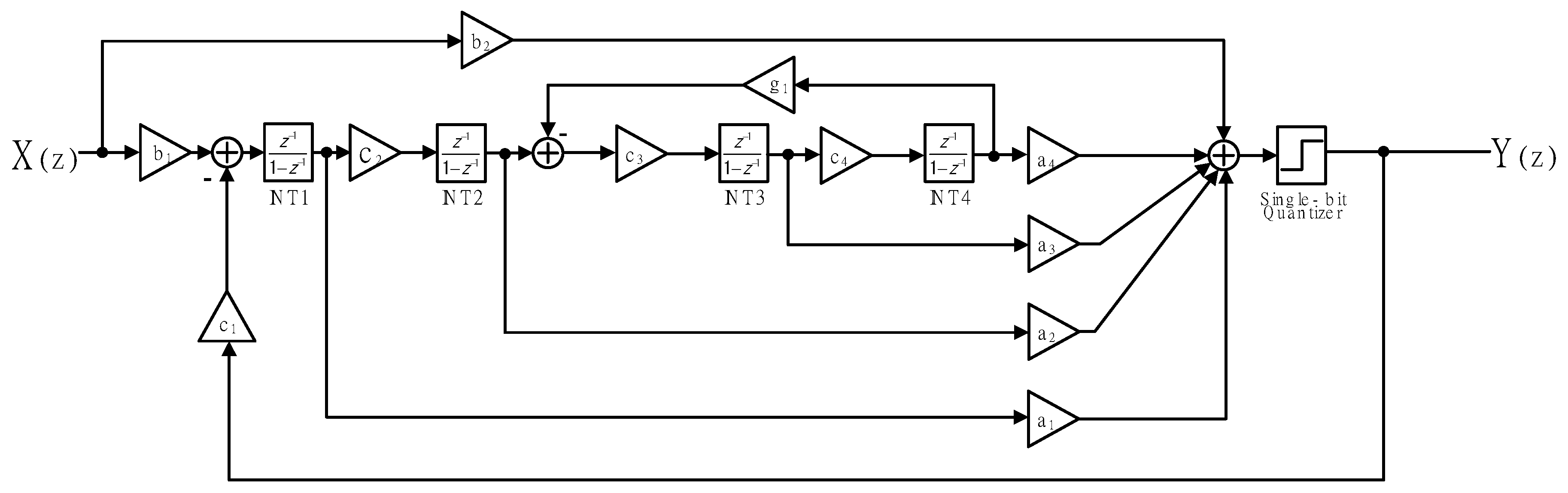
2.1. Fourth-Order CIFF DSM
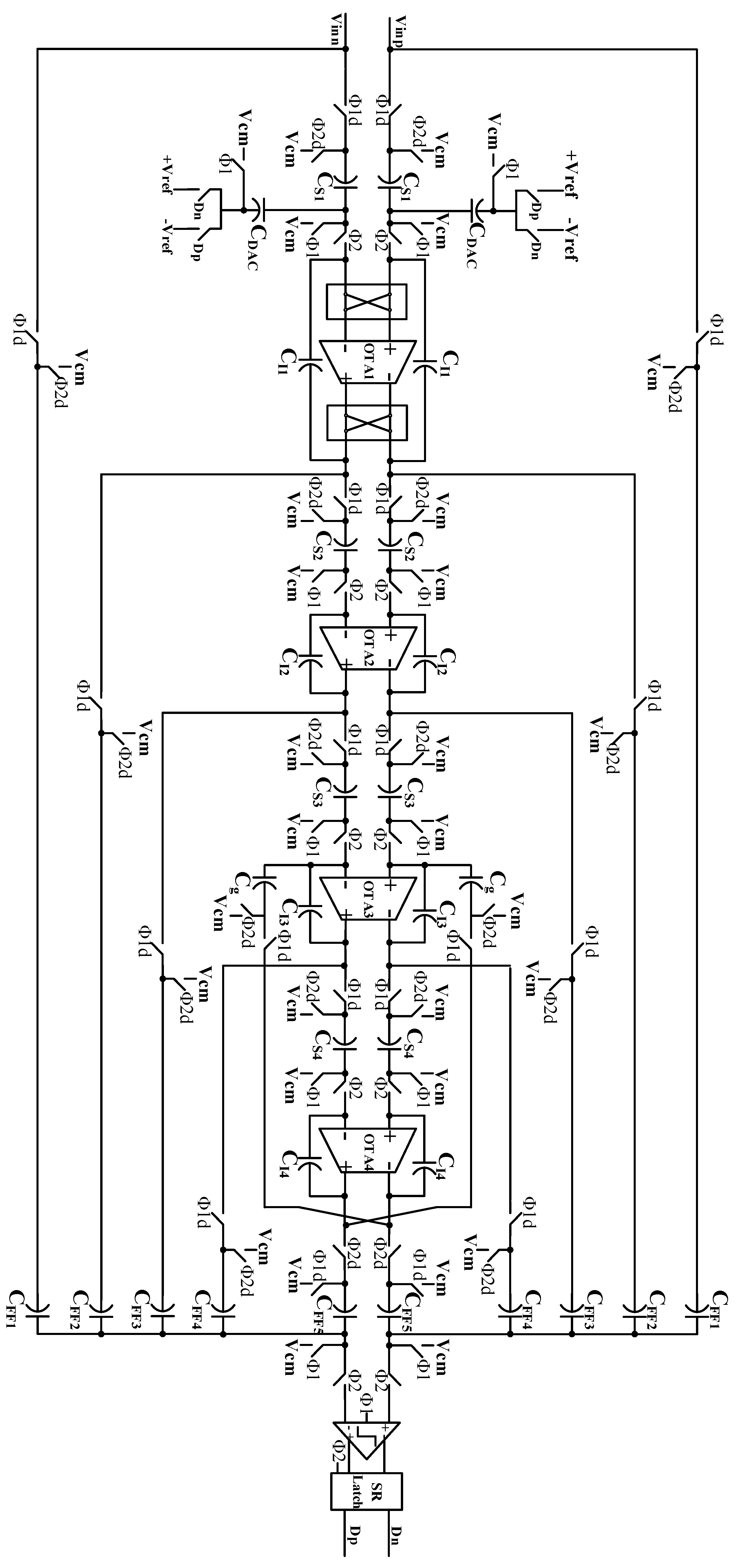
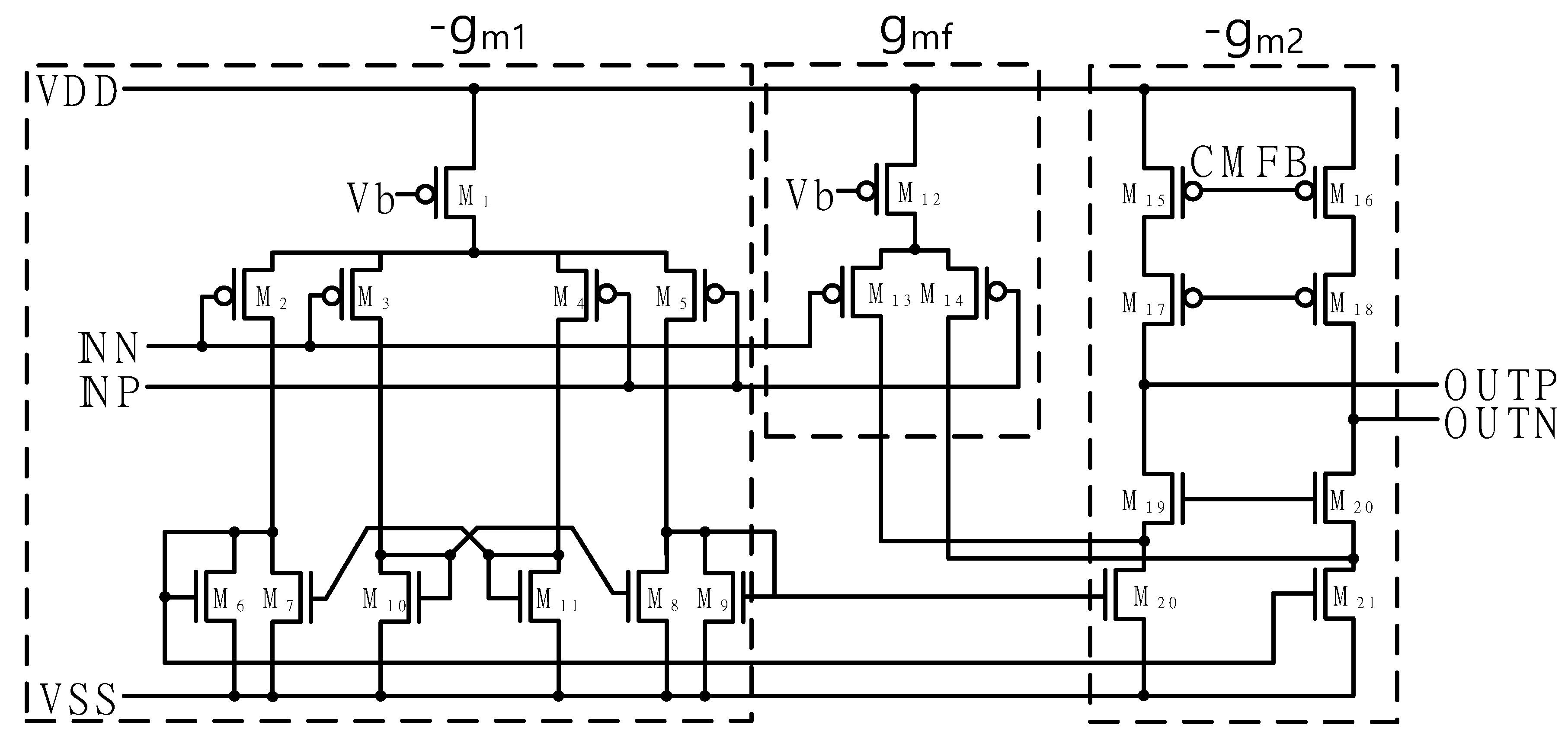
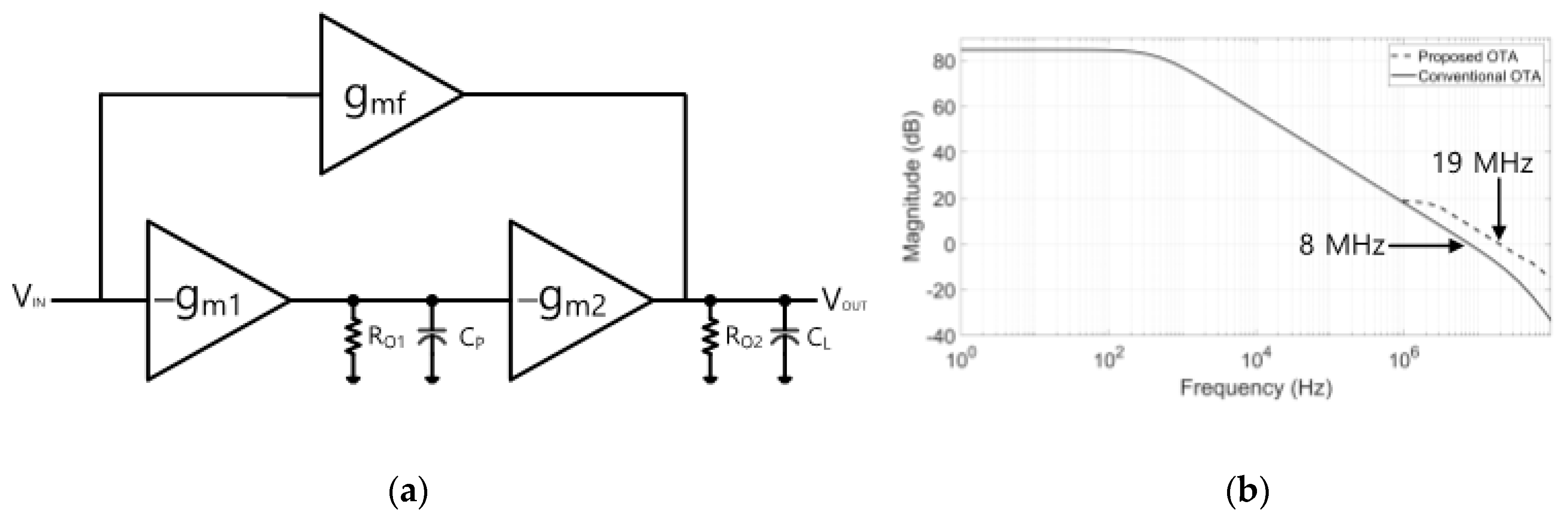
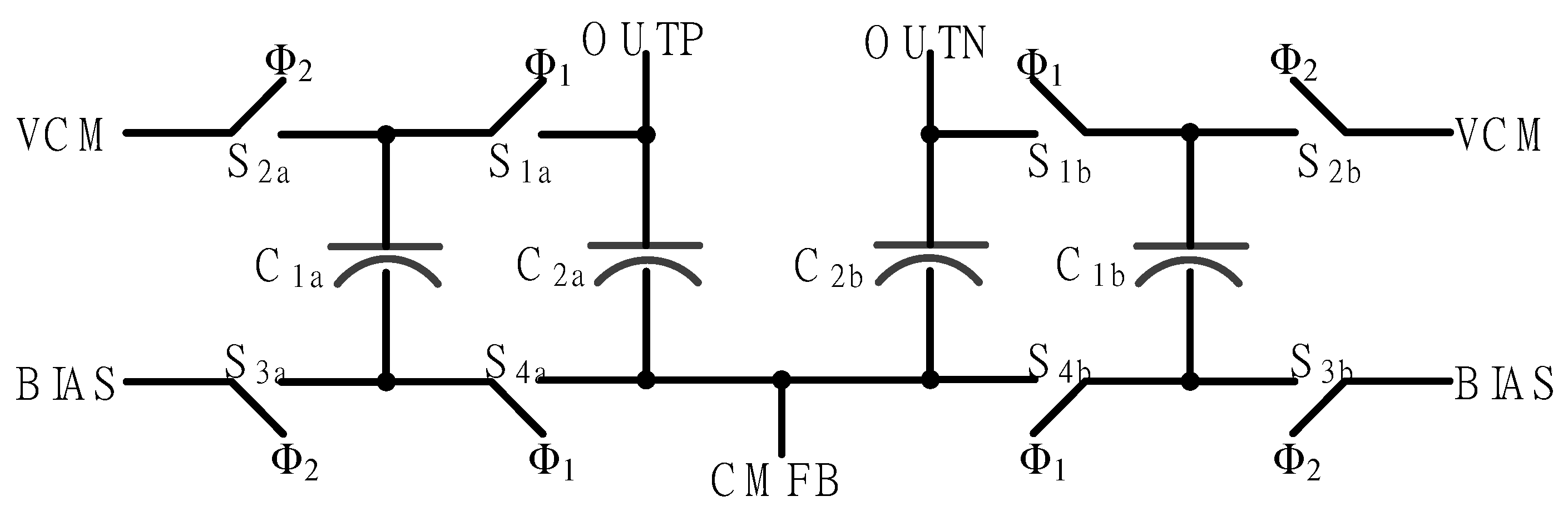
2.2. Proposed Feedforward OTA and Common-Mode Feedback (CMFB) Circuit
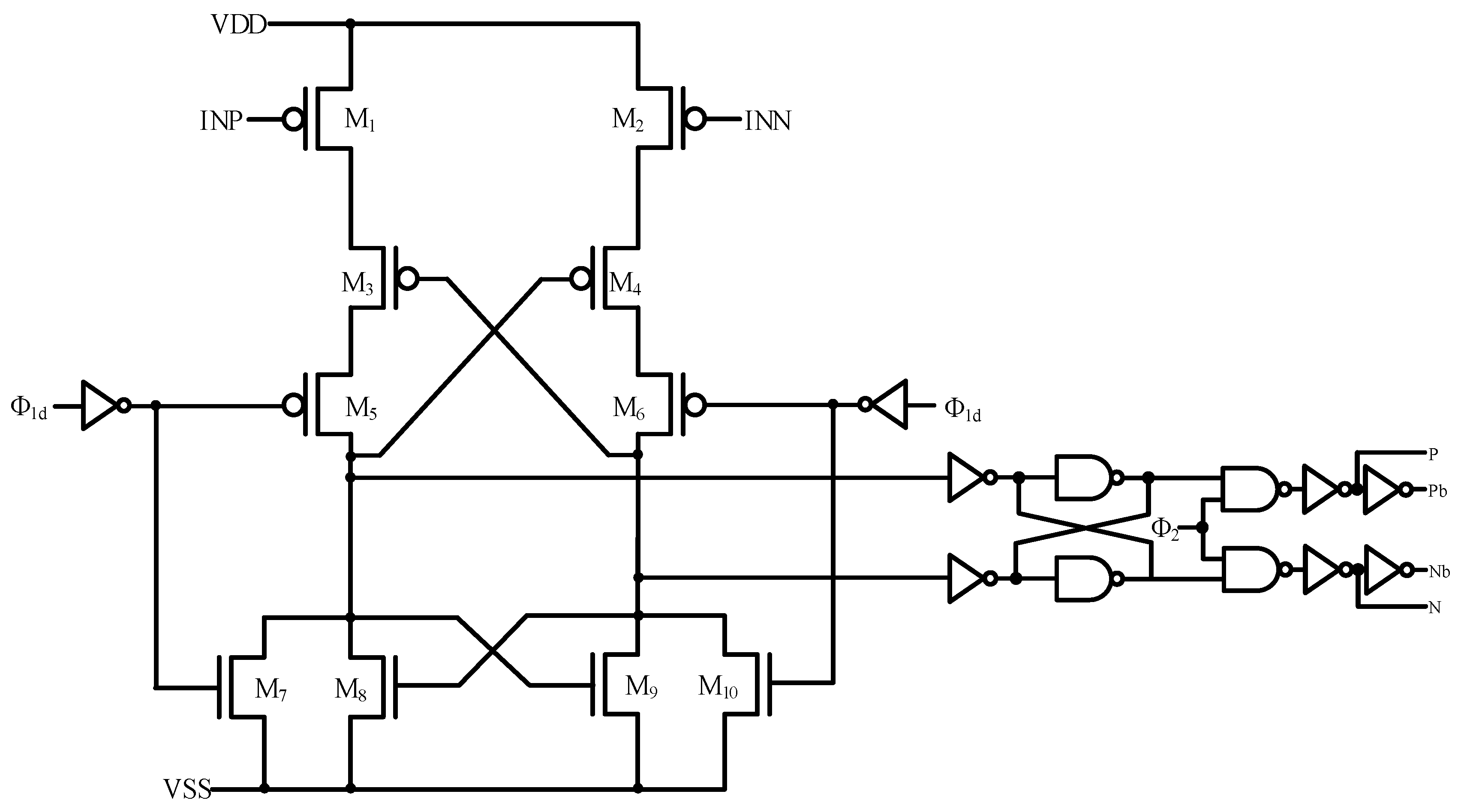
2.3. Single-Bit Quantizer
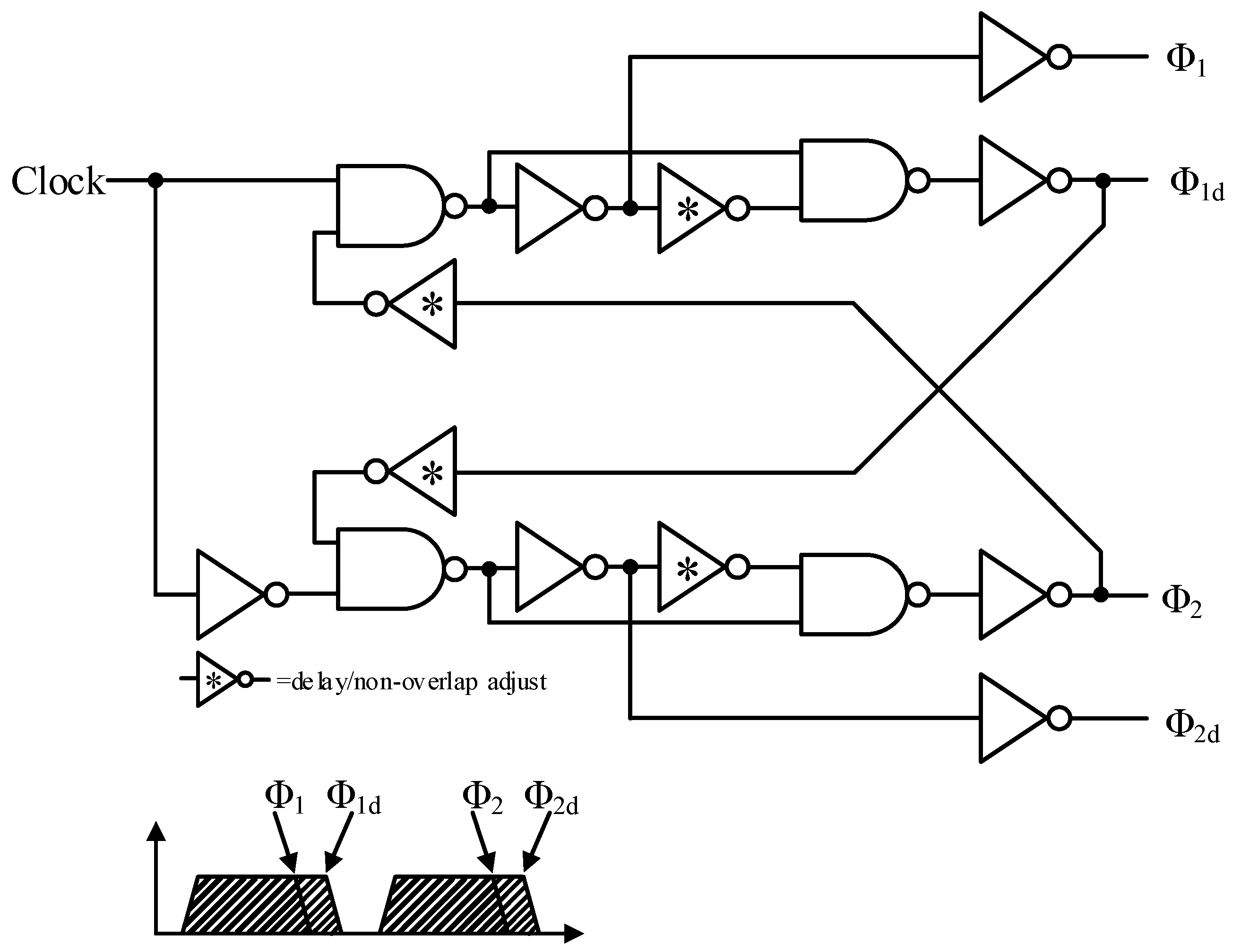
2.4. Clock Generator
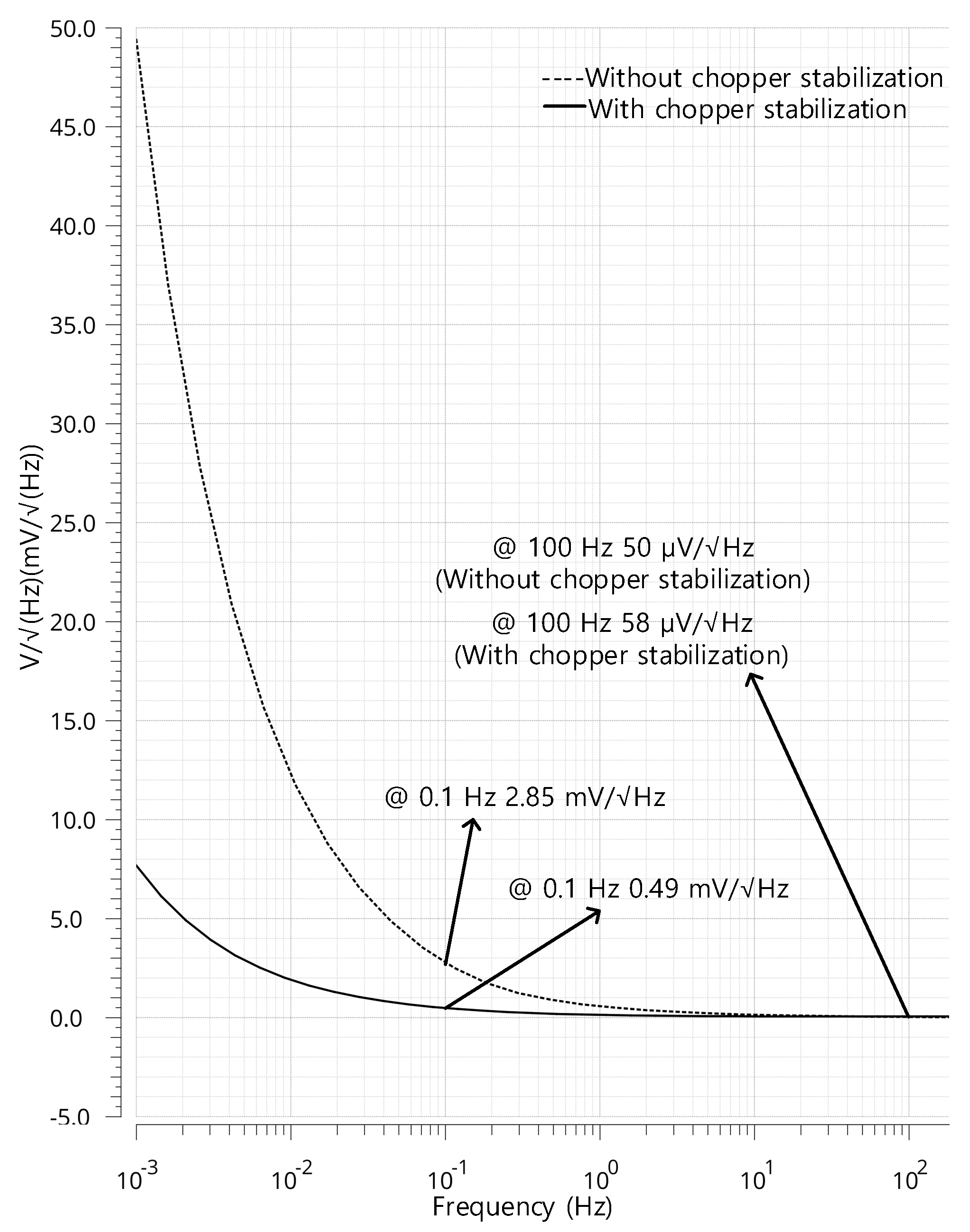
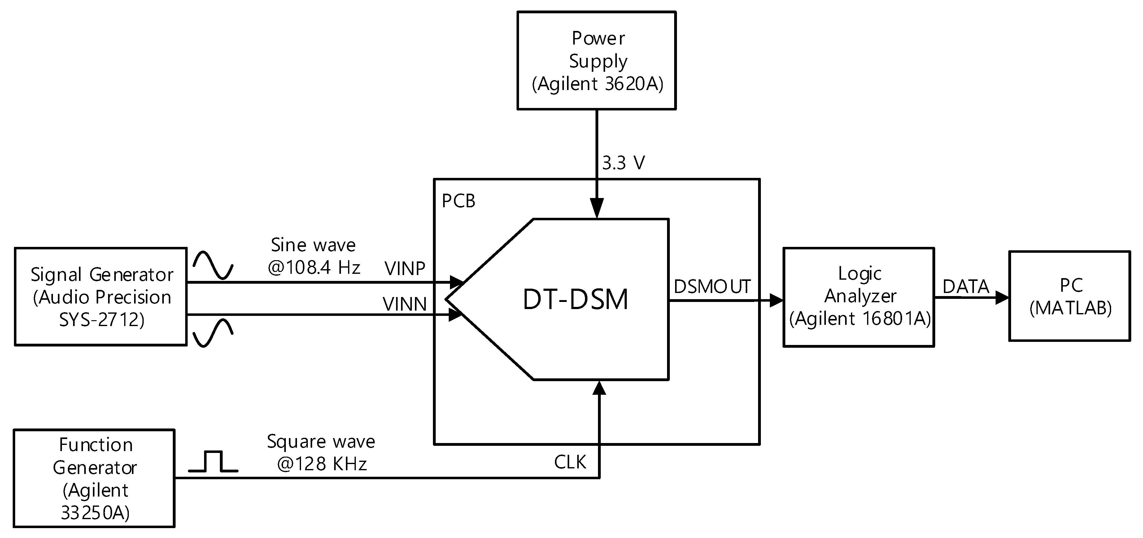
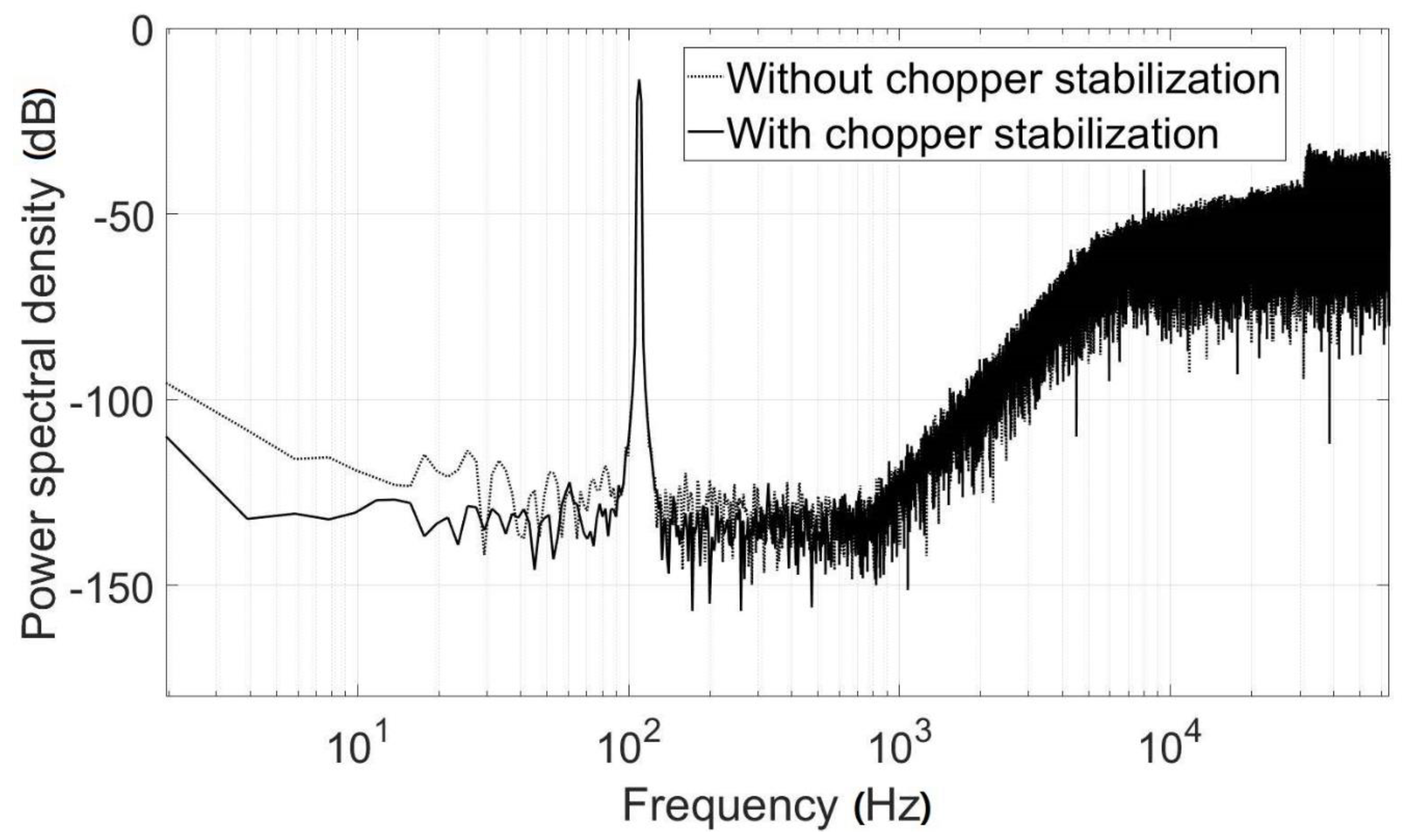
3. Experimental Results
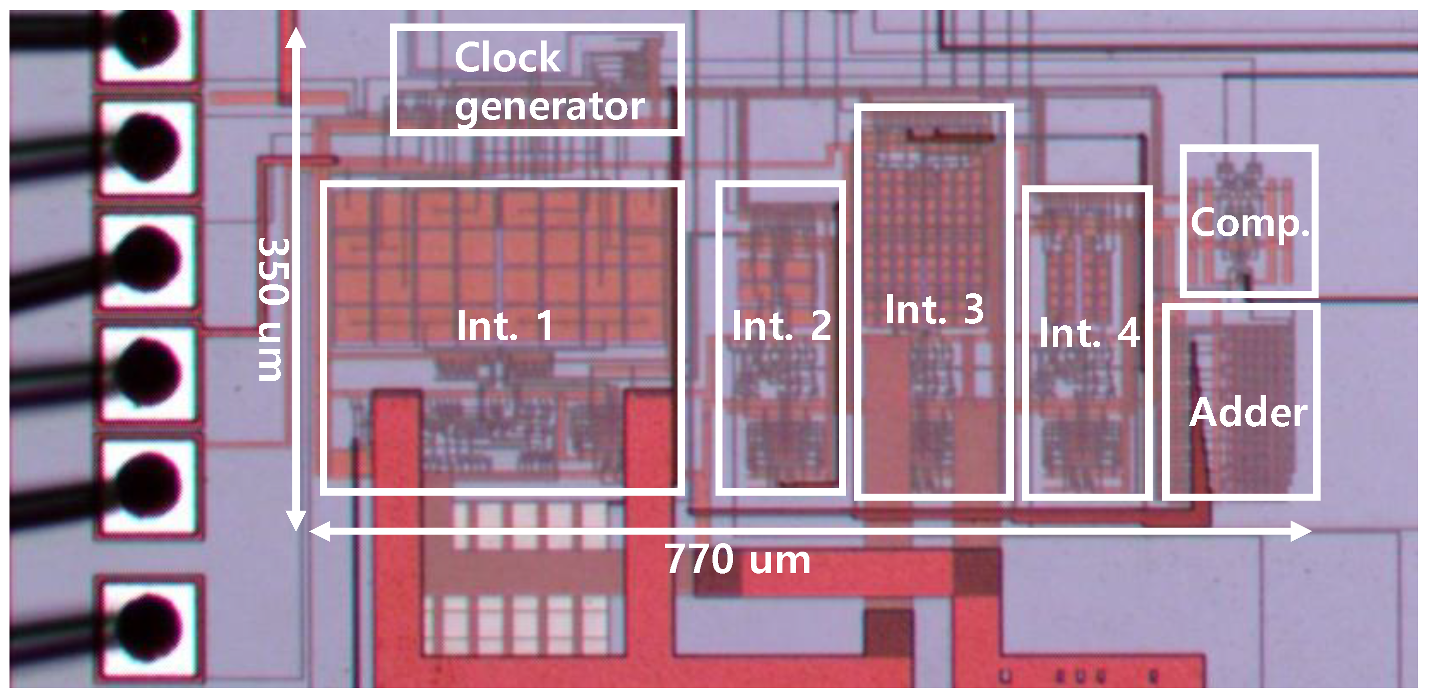
- The analog, digital, and mixed-signal parts were separated from each other to reduce attenuation caused by noise interference. Guard rings were also used for each part.
- Separate power supplies were used for the analog, digital, and mixed-signal parts, each with their bonding pad and chip package pin for the analog, digital, and mixed signal parts as well as the guard rings [19]. Separate power supplies were used for the analog, digital, and mixed-signal parts of the test board.
- The layout used a differential technique to reduce common mode interference [19]. The differential input transistors of the OTA were applied using the common centroid layout technique in order to improve matching performance.
4. Conclusions
Author Contributions
Funding
Acknowledgments
Conflicts of Interest
Abbreviations
| ADC | analog-to-digital converter |
| DSM | delta-sigma modulator |
| CT | continuous-time |
| DT | discrete-time |
| AFE | analog front-end |
| DR | dynamic range |
| CIFF | cascade-of-integrators with feedforward |
| CFIB | cascade-of-integrators with feedback |
| OTA | operational transconductance amplifier |
| SNR | signal-to-noise ratio |
| NTF | noise transfer function |
| NMOS | n-channel metal-oxide semiconductor |
| PMOS | p-channel metal-oxide semiconductor |
| SNDR | signal-to-noise and distortion ratio |
| UGBW | unity-gain bandwidth |
| CMFB | common-mode feedback |
| CMOS | complementary metal oxide semiconductor |
| SR | Set/Rest |
| NAND | Not-AND |
| dBFS | deciBels relative to Full Scale |
References
- Tang, X.; Hu, Q.; Tang, W. Delta–Sigma Encoder for Low-Power Wireless Bio-Sensors Using Ultrawideband Impulse Radio. IEEE Trans. Circuits Syst. Express Briefs 2017, 64, 747–751. [Google Scholar] [CrossRef]
- Leene, L.B.; Constandinou, T.G. A 0.016 mm2 12 b ΔΣ SAR With 14 fJ/conv. for Ultra Low Power Biosensor Arrays. IEEE Trans. Circuits Syst. Regul. Pap. 2017, 64, 2655–2665. [Google Scholar] [CrossRef]
- Shui, B.; Keller, M.; Kuhl, M.; Manoli, Y. A 70.8 dB 0.0045 mm2 low-power continuous-time incremental delta-sigma modulator for multi-site neural recording interfaces. In Proceedings of the 2018 IEEE International Symposium on Circuits and Systems (ISCAS), Florence, Italy, 27–30 May 2018; pp. 1–4. [Google Scholar]
- Gerfers, F.; Ortmanns, M. Continuous-Time Sigma-Delta A/D Conversion: Fundamentals, Performance Limits and Robust Implementations; Springer: Berlin, Germany, 2006. [Google Scholar]
- Webster, J.G. Medical Instrumentation: Application and Design, 4th ed.; John Wiley & Sons: New York, NY, USA, 2009. [Google Scholar]
- Desel, T.; Reichel, T.; Rudischhauser, S.; Hauer, H. A CMOS nine channel ECG measurement IC. In Proceedings of the 2nd International Conference on ASIC, Shanghai, China, 21–24 October 1996; pp. 115–118. [Google Scholar]
- Xu, J.; Zhao, M.; Wu, X.; Islam, M.K.; Yang, Z. A High Performance Delta-Sigma Modulator for Neurosensing. Sensors 2015, 15, 19466–19486. [Google Scholar] [CrossRef] [PubMed]
- Roh, J.; Byun, S.; Choi, Y.; Roh, H.; Kim, Y.-G.; Kown, J.-K. A 0.9-V 60-mW 1-bit fourth-order delta–sigma modulator with 83-dB dynamic range. IEEE J. Solid-State Circuits 2008, 43, 361–370. [Google Scholar] [CrossRef]
- Wang, Z.; Jung, Y.; Roh, J. A 10-MHz multi-bit MASH delta–sigma modulator with analog summing interstage. Analog. Integr. Circuits Signal Process. 2015, 85, 201–207. [Google Scholar] [CrossRef]
- Yoon, Y.; Choi, D.; Roh, J. A 0.4 V 63 μW 76.1 dB SNDR 20 kHz Bandwidth Delta-Sigma Modulator Using a Hybrid Switching Integrator. IEEE J. Solid-State Circuits 2015, 50, 2342–2352. [Google Scholar] [CrossRef]
- Jung, Y.; Roh, H.; Roh, J. An Input-Feedforward Multibit Adder-Less Δ−Σ Modulator for Ultrasound Imaging Systems. IEEE Trans. Instrum. Meas. 2013, 62, 2215–2227. [Google Scholar] [CrossRef]
- Yang, Y.; Chokhawala, A.; Alexander, M.; Melanson, J.; Hester, D. A 114-db 68-mW chopper-stabilized stereo multibit audio ADC in 5.62 mm2. IEEE J. Solid-State Circuits 2003, 38, 2061–2068. [Google Scholar] [CrossRef]
- De La Rosa, J.M.; Escalera, S.; Perez-Verdu, B.; Medeiro, F.; Guerra, O.; Del Rio, R.; Rodriguez-Vazquez, A. A CMOS 110-dB@40-kS/s programmable-gain chopper-stabilized third-order 2-1 cascade sigma-delta Modulator for low-power high-linearity automotive sensor ASICs. IEEE J. Solid-state Circuits 2005, 40, 2246–2264. [Google Scholar] [CrossRef]
- Razavi, B. Design of Analog CMOS Integrated Circuits, 2nd ed.; McGraw-Hill: New York, NY, USA, 2016. [Google Scholar]
- Bolatkale, M.; Breems, L.J.; Makinwa, K.A.A. High Speed and Wide Bandwidth Delta-Sigma ADCs; Springer International Publishing: New York, NY, USA, 2014. [Google Scholar]
- Roh, H.; Choi, Y.; Roh, J. A 89-dB DR 457-μW 20-kHz bandwidth delta-sigma modulator with gain-boosting OTAs. Analog Integr. Circuits Signal Process. 2010, 64, 173–182. [Google Scholar] [CrossRef]
- Geerts, Y.; Steyaert, M.; Sansen, W.M. Design of Multi-Bit Delta-Sigma A/D Converters; Springer: New York, NY, USA, 2006. [Google Scholar]
- Baker, R.J. CMOS: Circuit Design, Layout, and Simulation, 3rd ed.; IEEE Press: Hoboken, NJ, USA, 2019. [Google Scholar]
- José, M.; de la, R.; Rocio, D.R. CMOS Sigma-Delta Converters: Practical Design Guide; John Willy & Sons: Hoboken, NJ, USA, 2013. [Google Scholar]
- Lv, R.; Chen, W.; Liu, X. A High-Dynamic-Range Switched-Capacitor Sigma-Delta ADC for Digital Micromechanical Vibration Gyroscopes. Micromachines 2018, 9, 372. [Google Scholar] [CrossRef] [PubMed]
- Min, D.-J.; Shim, J.H. A Charge-Sharing-Based Two-Phase Charging Scheme for Zero-Crossing-Based Integrator Circuits. Electronics 2019, 8, 821. [Google Scholar] [CrossRef]
- Park, J.-E.; Hwang, Y.-H.; Jeong, D.-K. A 0.4-to-1 V Voltage Scalable ΔΣ ADC With Two-Step Hybrid Integrator for IoT Sensor Applications in 65-nm LP CMOS. IEEE Trans. Circuits Syst. Express Briefs 2017, 64, 1417–1421. [Google Scholar] [CrossRef]


| Input Coefficients | Feedforward Coefficients | Integrator Coefficients |
|---|---|---|
| b1 = 0.2 | a1 = 4 | c1 = 0.2 |
| b2 = 1 | a2 = 3 | c2 = 0.5 |
| c3 = 4/9 | ||
| c4 = 0.1 | ||
| g1 = 0.0003 |
| Sampling Capacitor | Integrating Capacitor | Feedforward Capacitor |
|---|---|---|
| CS1 = 2.5 | CF1 = 12.5 | CFF1 = 1 |
| CS2 = 0.5 | CF2 = 1 | CFF2 = 0.4 |
| CS3 = 0.8 | CF3 = 1.8 | CFF3 = 0.3 |
| CS4 = 0.1 | CF4 = 1 | CFF4 = 0.15 |
| CDAC = 2 | CFF5 = 0.15 |
| Parameter | First-Integrator’s OTA | Other OTAs |
|---|---|---|
| Supply voltage (V) | 3.3 | 3.3 |
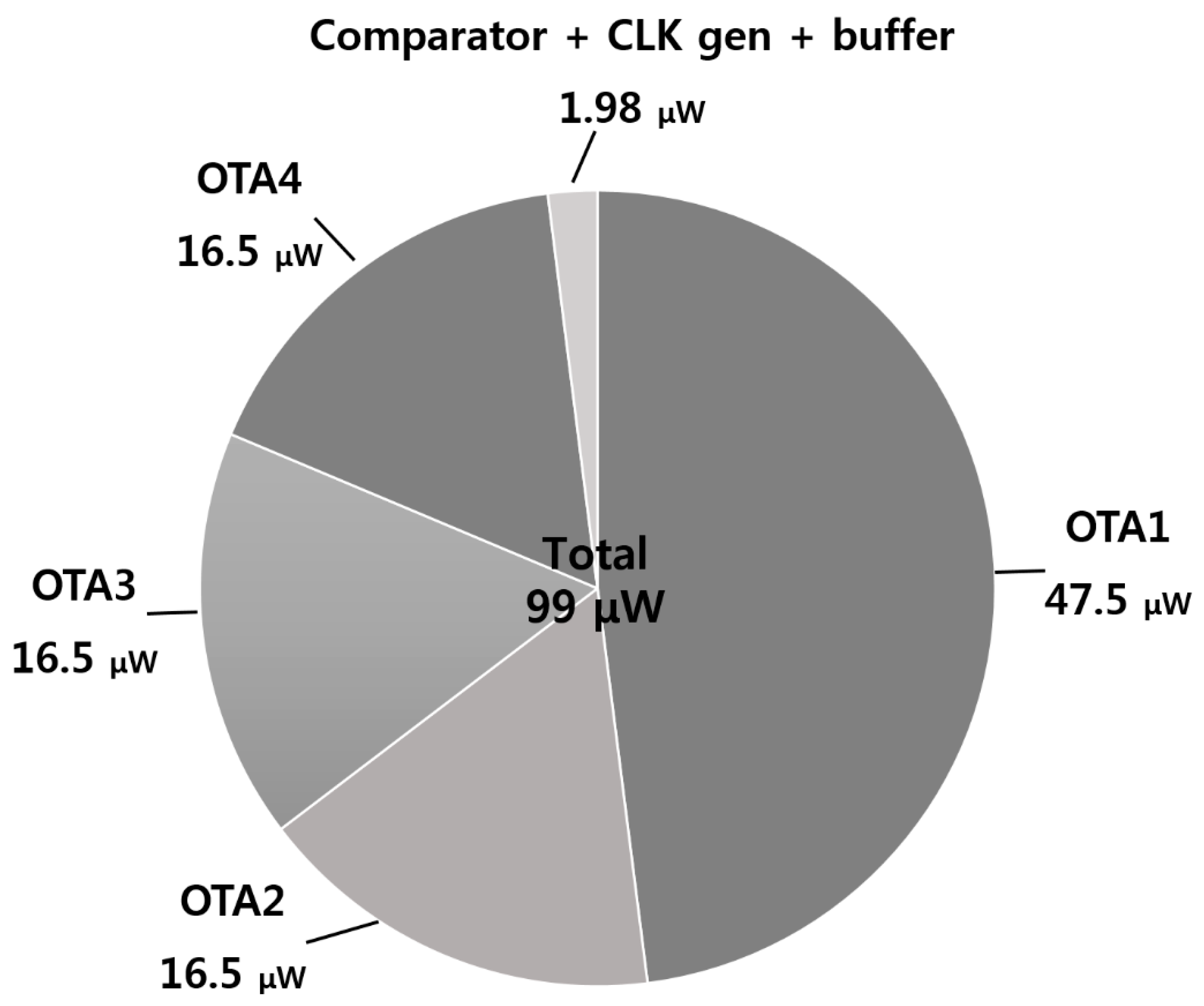
| Power consumption (W) | 14.4 | 5 |
| DC gain (dB) | 83 | 74 |
| Phase margin (degree) | 62 | 89 |
| Load capacitor (pF) | 2.2 | 0.9 |
| UGBW (MHz) | 18 | 2.6 |
| Parameter | Value | |
|---|---|---|
| Supply voltage (V) | 3.3 | 3.3 |
| Signal bandwidth (Hz) | 500 | 700 |
| Sampling frequency (kHz) | 128 | 128 |
| Power consumption (W) | 14.4 | 5 |
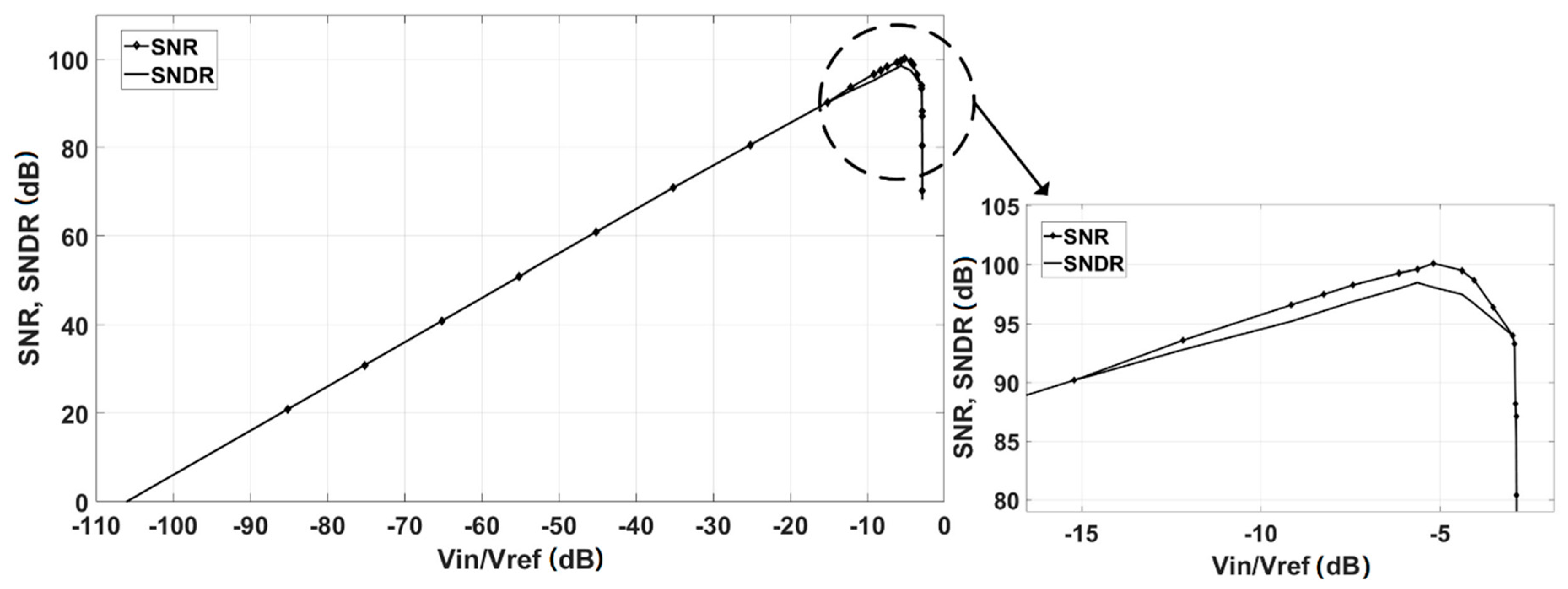
| Peak SNR (dB) | 100.3 | 99.7 |
| Peak SNDR (dB) | 98.5 | 98 |
| Dynamic range (dB) | 103 | 102.3 |
| Paper | This Work | Reference [20] | Reference [21] | Reference [22] | |
|---|---|---|---|---|---|
| Type | 1 bit DT | 1 bit DT | 1 bit DT | 1 bit DT | |
| Bandwidth (Hz) | 500 | 700 | 2000 | 2000 | 25,000 |
| Sampling frequency (kHz) | 128 | 2000 | 10,000 | 2048 | |
| Peak SNDR (dB) | 98.5 | 98 | 100.2 | 46.3 | 60.8 |
| DR (dB) | 100.3 | 107.6 | 56 | 70.1 | |
| VDD (V) | 3.3 | 5 | 1.8 | 0.5 | |
| Power consumption (W) | 99 | 3200 | 684 | 43.4 | |
| Process ( | 0.35 | 0.35 | 0.18 | 65 | |
| FOM (pJ/step) | 1.44 | 1.08 | 9.5 | 13.2 | 1.21 |
© 2019 by the authors. Licensee MDPI, Basel, Switzerland. This article is an open access article distributed under the terms and conditions of the Creative Commons Attribution (CC BY) license (http://creativecommons.org/licenses/by/4.0/).
Share and Cite
Lee, J.; Song, S.; Roh, J. A 103 dB DR Fourth-Order Delta-Sigma Modulator for Sensor Applications. Electronics 2019, 8, 1093. https://doi.org/10.3390/electronics8101093
Lee J, Song S, Roh J. A 103 dB DR Fourth-Order Delta-Sigma Modulator for Sensor Applications. Electronics. 2019; 8(10):1093. https://doi.org/10.3390/electronics8101093
Chicago/Turabian StyleLee, Jaeseong, Seokjae Song, and Jeongjin Roh. 2019. "A 103 dB DR Fourth-Order Delta-Sigma Modulator for Sensor Applications" Electronics 8, no. 10: 1093. https://doi.org/10.3390/electronics8101093
APA StyleLee, J., Song, S., & Roh, J. (2019). A 103 dB DR Fourth-Order Delta-Sigma Modulator for Sensor Applications. Electronics, 8(10), 1093. https://doi.org/10.3390/electronics8101093