1. Introduction
In recent decades, insulated gate bipolar transistor (IGBT) modules are more common in automotive and rail-traction applications due to its excellent performance in switching speeds, conduction losses, and over-current capacity [
1,
2,
3]. However, with the improvement of power density and the worsening thermal environment, there may generate large and unpredictable temperature fluctuations in the device. The temperature fluctuations may deteriorate the electrical specification and lead to different degrees of thermo-mechanical failure, which have a serious influence on the reliability of the power conversion system [
4,
5]. Therefore, temperature control and thermal management become more of a concern [
6].
The pre-condition of temperature control and thermal management is the accurate measurement of device junction temperature. Junction temperature is a key parameter that influence both the performance and the reliability of the device [
7,
8]. With the accurate junction temperature, we can push the device operating temperature to its limitations to realize the over-temperature protection. In addition, we can also use junction temperature as an indicator of the health condition monitoring and lifetime prediction of the power conversion stage. Consequently, the junction temperature measurement have aroused interest from both device manufacturers and users.
Existing junction temperature measurement approaches consist of an optimal method, electrical method, and physical-contacting method [
9,
10]. Infrared (IR) cameras [
11,
12], optical fiber [
13], IR microscope [
14,
15] are representative of the optical method, and have the ability to directly obtain a temperature map of the device, while the measuring equipment is expensive and requires additional modification compared with a standard module package. For these reasons, the electrical method is often preferred, since it employs the device itself as a temperature sensor and has no need to modify the packaging structure. Using a temperature-sensitive electrical parameter (TSEP), such as collector-emitter on-state voltage (
), gate-emitter threshold voltage (
), switch turn ON (
) and turn OFF (
) time, the junction temperature measurements can be performed [
9]. Nevertheless, electrical method face many challenges in online implementation, such as the need to compensate the operation conditions and the need for high-precision measurement circuit, limiting the practical applications of this method [
16,
17]. The typical physical-contacting method is electro-thermal model. Compared with the optical and electrical method, the electro-thermal model just needs the device power losses and the case temperature to obtain the junction temperature. Thus, considering the problems of cost and on-line implementation, the electro-thermal model may be more suitable to measure the junction temperature [
18,
19,
20,
21]. In this paper, we will focus on research about the electro-thermal model.
In the past five years, a significant number of research articles for improving the performance of electro-thermal models have been presented. For example, in [
19,
20,
22,
23,
24], the authors proposed the finite element method (FEM) and finite difference method (FDM) to solve the problems of thermal couplings and boundary conditions. In [
25,
26,
27,
28], the authors proposed Fourier series-based thermal models with the information of physical structure and material properties to deal with the issues of computational intensity and accuracy. Unfortunately, these studies pay little attention to the device aging effect to the electro-thermal models. The gradual degradation of the device due to solder fatigue increases the thermal impedance across the thermal path, which leads to the mismatch between the model parameters and the fatigue device. In this condition, the estimated junction temperature from the electro-thermal model may be far less than the actual junction temperature. Moreover, the actual junction temperature may exceed the threshold temperature of the chip, which may cause thermo-electrical breakdown, local thermal runaway, and thermo-mechanical failure.
To address the aforementioned issues, it is necessary to build an improved electro-thermal model which is independent of solder fatigue to develop a more reliable power conversion system. Some current research has paid attention to this practical issue. In [
29,
30], the changes of thermal impedance caused by solder fatigue is assessed and used to update the parameters of the electro-thermal model. Nevertheless, this process has to be off-line to eliminate the effect of operation conditions on the measurement circuit. In addition, another main issue is how to find solder fatigue in time and update the model parameters accordingly. In [
31], the actual junction temperature during solder fatigue conditions is obtained via the on-state collector-emitter voltage
, and used to update the model parameters, while the measurement of
requires an additional high-precision circuit, making this method costly. Thus, the weaknesses described above make the existing means conservative.
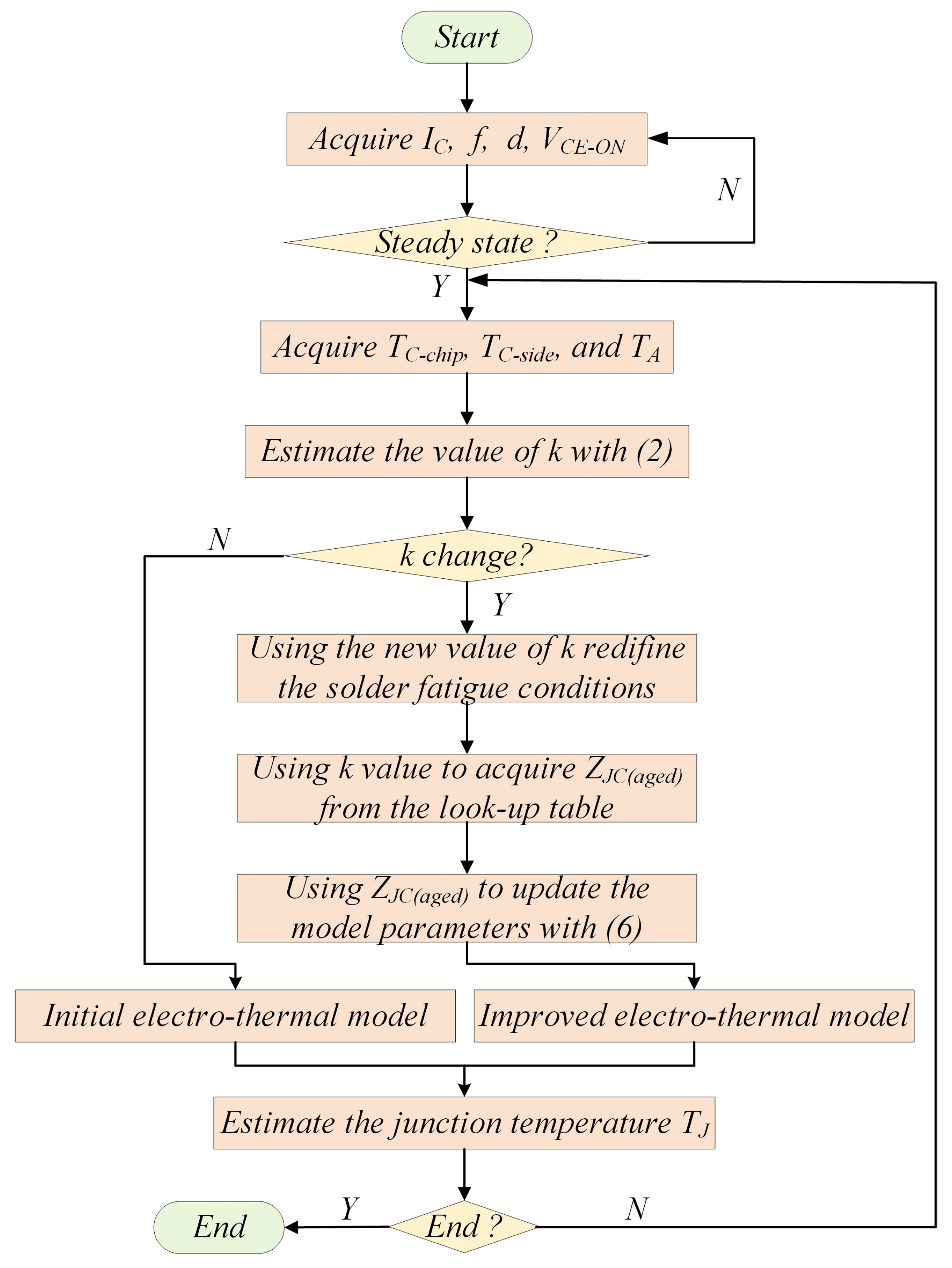
Motivated by the analysis described above, in this paper, an improved electro-thermal model which is able to monitor solder fatigue in time and update model parameters accordingly is proposed. Two aspects of the work are demonstrated: (a) solder fatigue is monitored with the measured case temperatures; (b) and when solder fatigue is detected, the model parameters is updated to match with the fatigue device according to the linear thermal characteristics. With the combinations of the above two parts, the parameters of the electro-thermal model can be updated in time and the accuracy of junction temperature estimate can be recovered. Consequently, the reliability performance of IGBT modules can be improved.
This paper is organized as follows.
Section 2 introduces the mechanism of solder fatigue and proposes a new parameter that is based on the case temperatures to monitor solder fatigue conditions in real time. In
Section 3, the update of electro-thermal model parameters is performed to match the model parameters with the fatigue device. In
Section 4, the implementation of the proposed method is presented. An experimental study is provided in
Section 5 to verify the effectiveness of the proposed method. Conclusions are drawn in
Section 6.
2. Analysis and Monitoring of Solder Fatigue
By monitoring solder fatigue in real time, we can find solder fatigue timely and then update the model parameters accordingly to reduce the unreliable operation time of the device. In this section, the fatigue mechanism of the solder is analyzed and a new parameter depending on the case temperature is proposed to monitor solder fatigue in real time.
2.1. Analysis of Solder Fatigue
Figure 1 shows a cross-sectional view of a commercial IGBT module, which consists of IGBT and diode chips, direct-bond-copper (DBC) substrate, solder and copper baseplate. Typically, the DBC substrate including ceramic and metallized copper films is connected on the copper baseplate with the solder layer. The IGBT and diode chips are soldered onto the DBC substrate. With the aluminum bond wires, the chips are linked to the DBC copper. At last, the above parts are packaged in a plastic case, and encapsulated with silicon gel. In addition, there always have a thermal interface material (e.g., thermal grease) between the baseplate and heat sink to improve the performance of thermal transfer. At present, some low-power IGBT modules are designed with integrated heat sink, in this condition, the copper baseplate is unnecessary, reducing the manufacturing costs. Although the cost is reduced, the temperature difference across the device may increase, reducing the thermal overloading capability.
Due to the several materials with different coefficients of thermal expansion (CTEs) combined with temperature swings, thermo-mechanical stress between the solder layer and the adjacent layers, which is the main cause of solder fatigue, are generated. When the range of temperature swing is
, the thermo-mechanical stress
on the solder layer can be described as follows:
where
denotes the difference of CTEs between the solder layer and the adjacent layers.
Considering the temperature swings induced by the power cycles, the thermo-mechanical stress continues to operate on the solder layer, leading to solder fatigue, e.g., creep, voids, cracks or delamination in the solder layer [
32,
33,
34]. Compared with the material property of solder layer, the thermal conductivity of voids or cracks is small, while the specific heat is large, which can be seen in
Table 1. These features deteriorate the heat dissipation of the solder layer, leading to accumulation of heat inside the device. Eventually, the heat flux density in the device and thermal impedance across the heat transfer paths increase. Generally, the initial parameters of electro-thermal model is based on the healthy device. The above faults lead to the mismatch between the model parameters and the fatigue device. In this condition, the estimated junction temperature from the electro-thermal model may be far less than the actual junction temperature. In addition, the actual junction temperature may exceed the threshold temperature of the chip, which may cause thermo-electrical breakdown, local thermal runaway, and thermo-mechanical failure.
2.2. Monitoring of Solder Fatigue
The common means to monitor solder fatigue can be categorised into electrical-based method and thermal-based method. The electrical-based method is according to the changes of switching-related parameters of an IGBT, which is influenced by solder fatigue. The typical parameters, such as the inverter harmonic current and gate current, are always used to detect solder fatigue, while an additional high-accuracy circuit is necessary for the measurement of these parameters, making this type of method expensive. The thermal-based method is chosen according to the changes of temperature-related parameters of an IGBT, including the junction temperature and case temperature. Generally, the changes of temperature-related parameters are very slow, and therefore are easily obtained by a general circuit. Compared with the electrical-based method, the thermal-based method is more easily realized in practical applications. Thus, in this section, a new monitoring parameter based on the temperature-related parameters, i.e., the ratio between two case-to-ambient thermal resistance, is proposed to detect solder fatigue in real time.
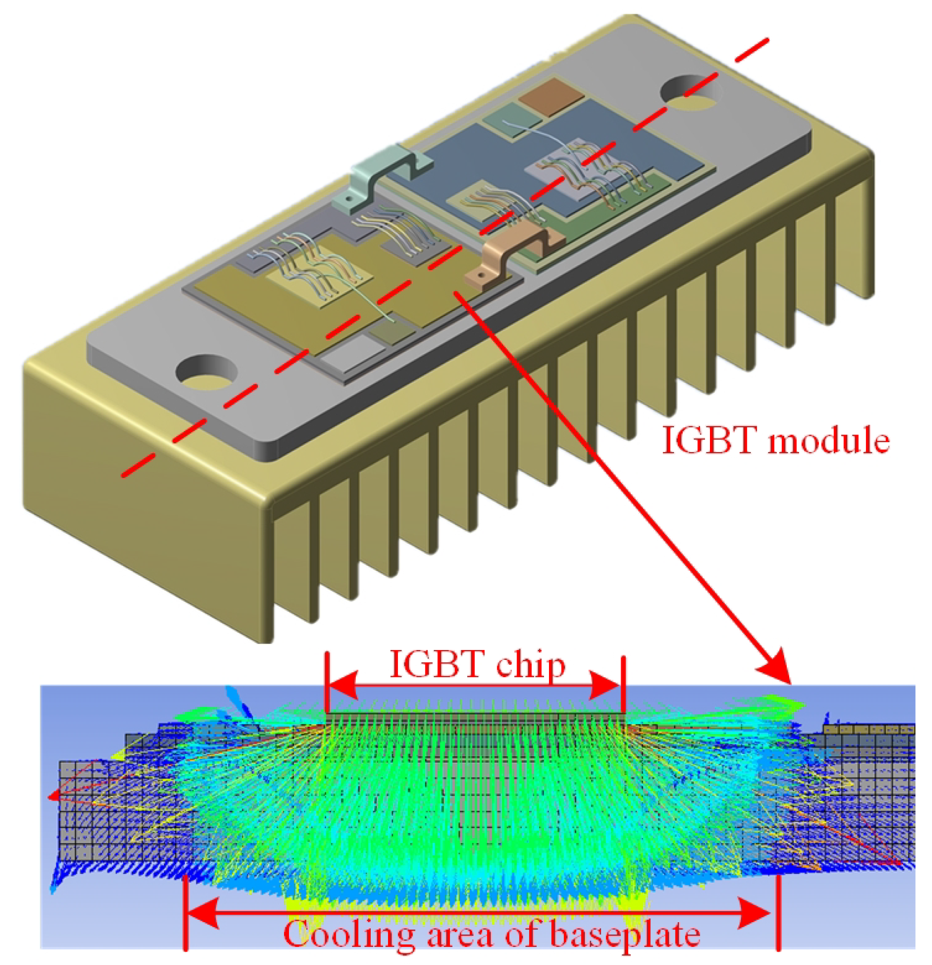
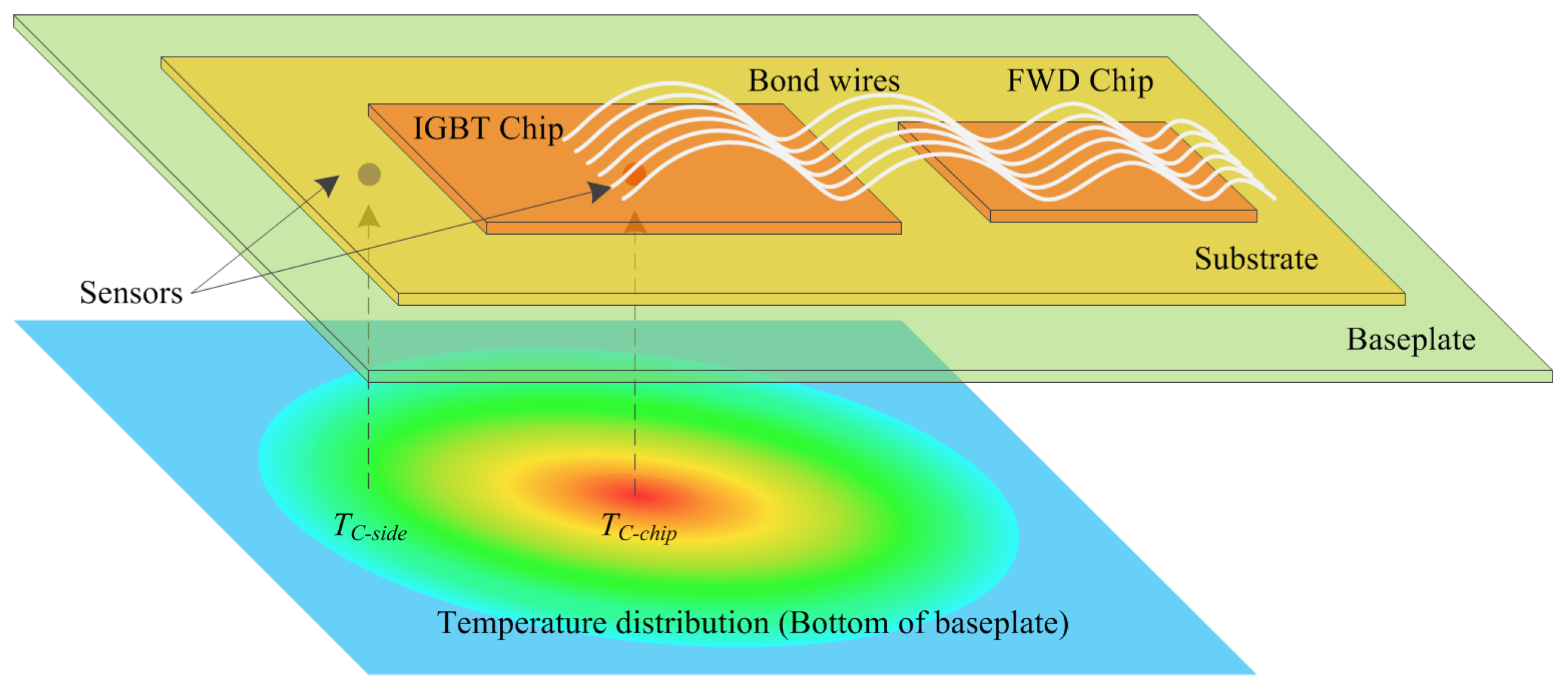
In the IGBT module, the heat is generally generated on the top surface of the chips, and then spreads down various layers to the bottom surface of the baseplate, as shown in
Figure 2, which is analyzed in ANSYS. It can be seen that the bottom surface of baseplate contains a larger temperature distribution area than the top surface of the chip. In addition, since most of the heat spreads down along with the vertical direction inside the module, which is known as the optimal path, the temperature in the central area is much higher than that of the rest area at the bottom surface of baseplate, leading to that the temperature distribution at the bottom surface of baseplate is non-uniform.
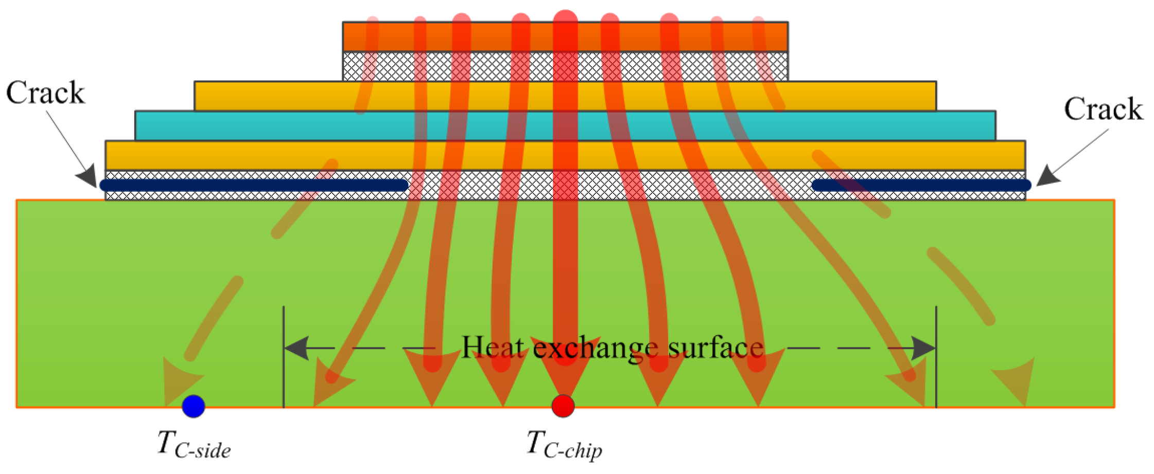
Solder fatigue indicates that the faults such as cracks or voids have formed in the solder layer. Due to the existance of the cracks or voids, the heat propagation area in the solder layer is shrunken, leading to the deterioration of the heat transfer inside the device. Since the cracks or voids always originate from the edge area of the solder layer and then propagate to the center, the heat has to transfer to the baseplate through the non-cracked area that located at the center of the solder layer. Consequently, the case temperature at the central area of baseplate increases steadily, while that of the rest area decreases, causing the changes of non-uniformity of temperature distribution at the bottom surface of baseplate. The above analysis indicates that the non-uniformity of temperature distribution of the baseplate is dependent on solder fatigue conditions, and therefore can be used to monitor the solder fatigue.
The non-uniformity of temperature distribution of the baseplate can be characterized by a ratio between two case-to-ambient thermal resistance. The case-to-ambient thermal resistance can be defined as follows:
where
denotes the case temperature of the baseplate,
denotes the ambient temperature,
P represents the power losses of the device.
Two typical case temperatures that are susceptible to solder fatigue are chosen, and are shown in
Figure 3. The first is
, which is most sensitive to the changes of heat flux inside the device, the second is
, where the cracks or voids originate. It should be noted that the heat generated at the top surface of the chip spreads down to the bottom surface of the baseplate with an angle of 45
. With this angle and the chip size, the temperature distribution area at the bottom surface of the baseplate can be estimated. The
site is located at the end of this temperature distribution area [
35,
36]. The ratio between the two thermal resistance is defined as
k, and estimated as follows:
The parameter k is able to characterize the impact of solder fatigue on the non-uniformity of the case temperature distribution. With the process of solder fatigue, increases due to the concentration of the heat flux, while decreases as its location tends to move outside of the heat propagation area, intensifying the non-uniformity of the case temperature distribution. Consequently, the value of k increases monotonously with increasing solder fatigue. The parameter k, which is only dependent on the case temperatures, is competent to detect solder fatigue conditions in real time.
3. Update of the Electro-Thermal Model Parameters
An improved electro-thermal model is necessary to guarantee the measurement accuracy of the junction temperature to improve the operational reliability of the power conversion system. The two typical types of electro-thermal model are the Cauer and Foster models, respectively. The parameters of Cauer model is based on the physical structure of the device and the material properties of various layers. If we want to update the Cauer model parameters, the changes of physical structure and material properties due to solder fatigue have to be assessed precisely, while this process is nearly impossible during the normal operation of device. The Foster model is an equipment model, and its parameters are fitted from the transient thermal impedance curve , that can be obtained by simulation or experiment process. The Foster model parameters can be updated according to the linear thermal property of the device, since there have a linear time-varying relationship between and solder fatigue. Compared with the Cauer model, the Foster model is more widely employed in practical applications and its parameters are more easily updated. Thus, in this section, we focus on the research of the parameters update of the Foster model.
The Foster model parameters consist of thermal resistance
and thermal capacitance
, and are defined as follows:
and
where
is the thickness of the
th layer.
,
and
are the thermal conductivity, specific heat capacity, and material density of the
th layer, respectively.
and
are the effective cross-section area and the effective volume of the
th layer, respectively.
The thermal resistance
identify the mean value of the junction temperature during the steady state, while the thermal capacitance
determines the dynamic behavior of the junction temperature. According to the research work in [
29], solder fatigue may have a stronger influence on the
than
, while in this section, we assume that solder fatigue has the same influence on
and
for modeling simplication.
The faults like cracks and voids deteriorate the heat dissipation of the solder layer, leading to the increase of the heat flux density in the device, and therefore the increase of the thermal impedance across the heat transfer paths, i.e.,
. The changes of
lead to the mismatch between the model parameters and the fatigue device. On the other hand, the model parameters are extracted from
. Therefore, the changes of
can be used to update the model parameters. According to the linear thermal property of the device, an approximate calculation to correlate
,
and the changes of
is proposed as follows:
and
where
is the aged thermal resistance,
is the aged capacitance and
is the aged thermal impedance of the device.
It can be seen from (
6) and (
7) that all the variables, except
, are known. Thus, the only thing we need to do is to acquire the information of
. It is difficult to obtain the value of
directly during the normal operation of the device, while we may employ an indirect way to obtain
. As described in Section II-B, the proposed monitoring parameter
k just relies on the conditions of solder fatigue, while it is independent of the operation conditions of the device. Meanwhile, the value of
also depends on solder fatigue conditions. Thus, the relationships between
k and
are unique, and can be easily established by an offline aging test [
37]. In practical applications, with the measured
k, the value of
can be obtained and used to update the model parameters.
5. Experimental Validation
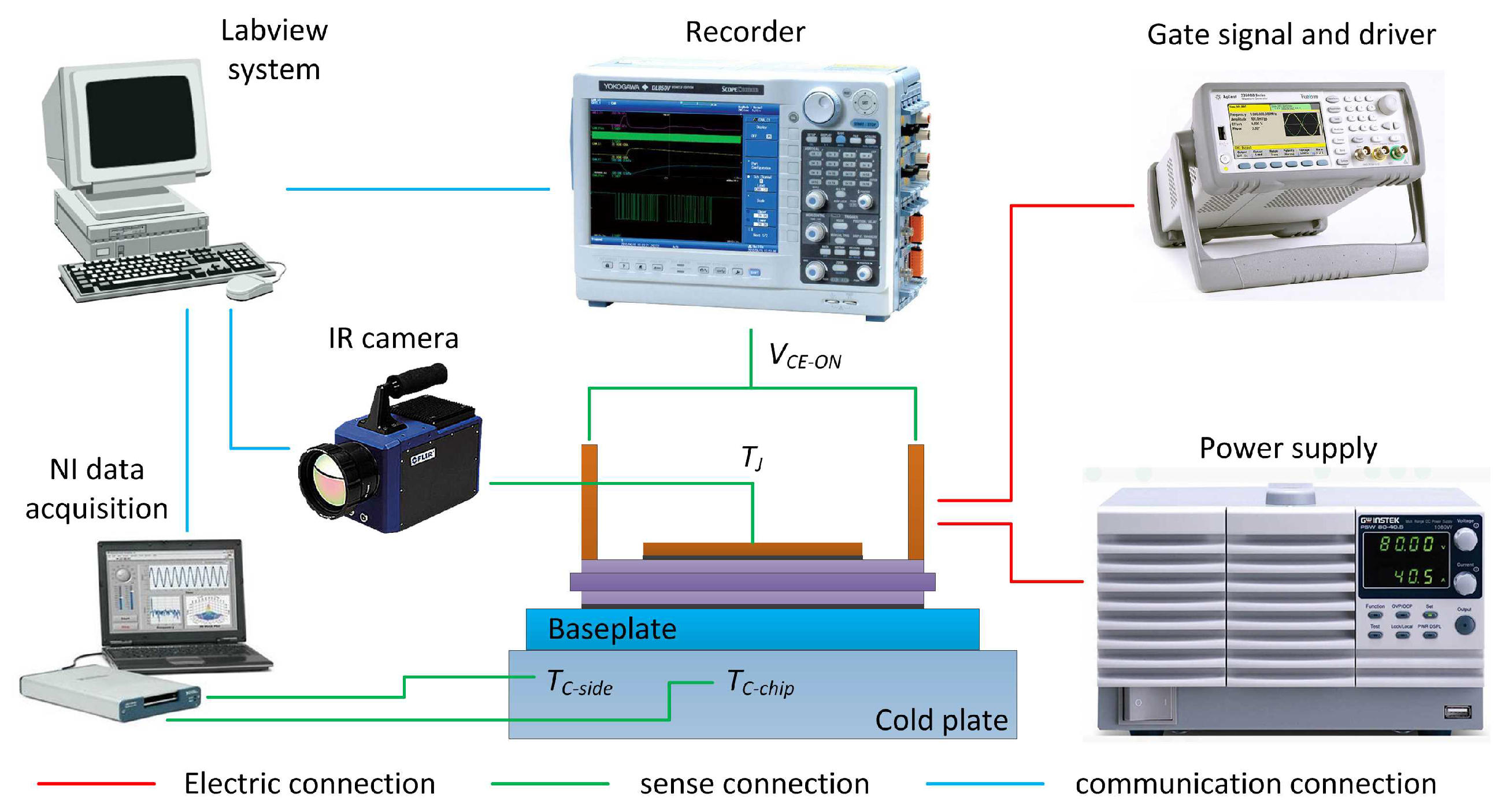
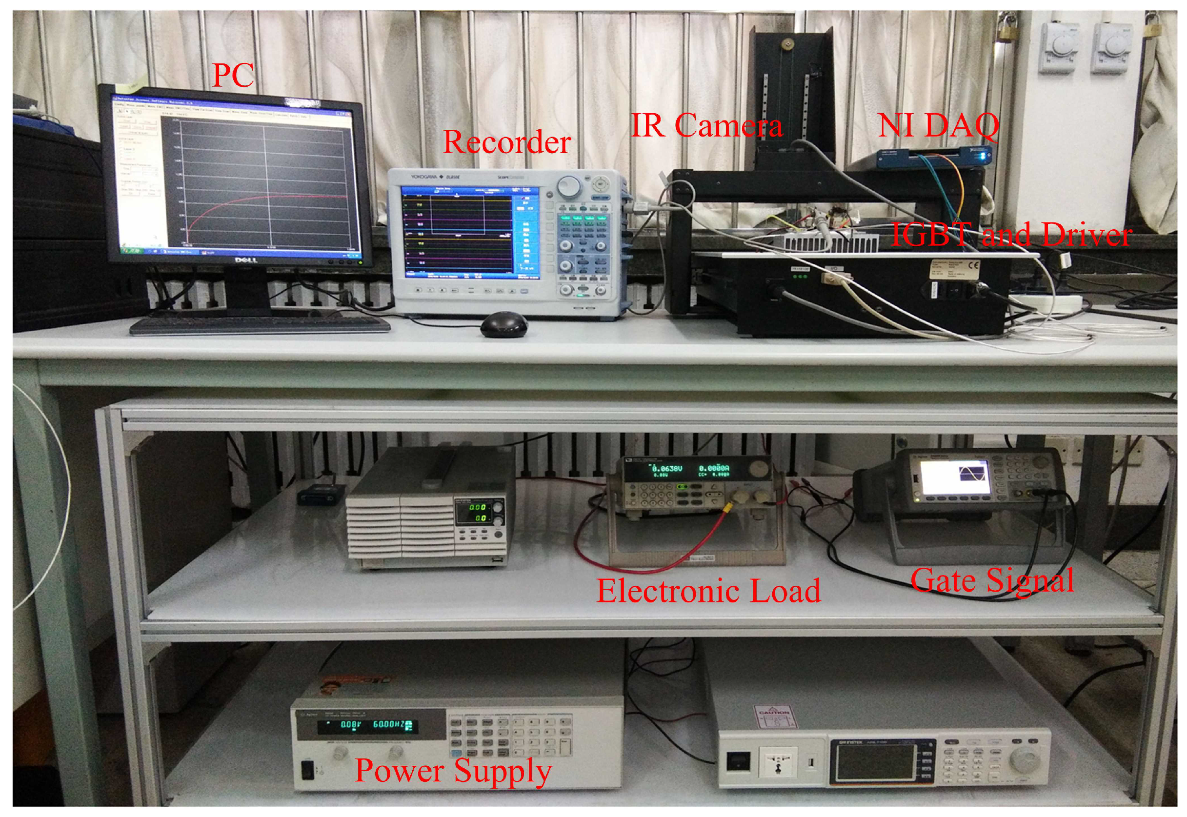
In this section, the effectiveness of the improved electro-thermal model, which is independent of solder fatigue, is demonstrated. The schematic of the experimental setup is presented in
Figure 6, and the actual experimental setup, which includes an IGBT module (SKM300GB128D, the silica gel is removed), an IR camera, a recorder, a gate driver, an AC power supply, an aluminum heat sink, and a National Instruments (NI) data acquisition instrument with thermal sensors, is shown in
Figure 7.
The design of the experimental analysis is performed as follows to eliminate the influence of various operation conditions: (a) the heat sink is cooled by forced-air convection, and the cooling surface keeps constant at 25 C; (b) the load current is sinusoidal current with an amplitude of 75 A; (c) the experimental analysis is processed in a transient mode for 100 s to reach a steady state. It should be noted that the major concern of this paper is the thermal behavior of the device induced by the various currents. Whether the sinusoidal current or the irregular currents and voltages with harmonics, they have the same influence on the thermal behavior of the device, i.e., generating power loss and increasing the material temperature inside the device. The difference between the sinusoidal current and the irregular currents with harmonics is the amount and/or the production rate of the power loss of the device. Based on this fact, the experimental validation are only processed in sinusoidal current.
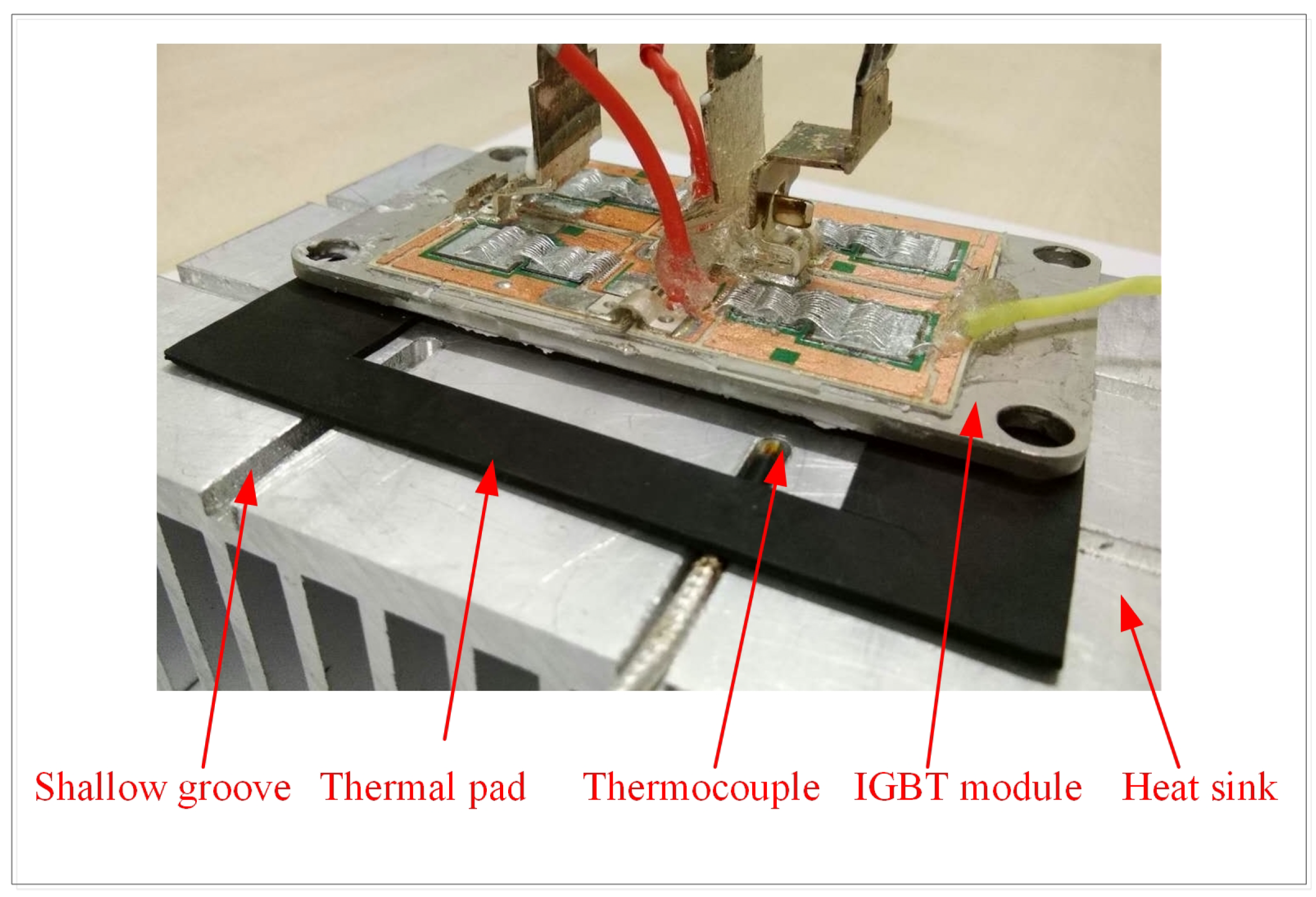
In addition, due to the complexity of the thermal aging test, in this section, the solder fatigue is simulated by a hollow thermal pad between the baseplate and the heat sink, as shown in
Figure 8. The thermal pad represents solder fatigue, while the hollow area filled with thermal grease represents the healthy condition. Six aging conditions are used to emulate the development of solder fatigue. 0% to 50% area of the solder layer are successively set to be fatigue with an interval of 10%, and shown in
Table 2. The results of the experimental test are described next.
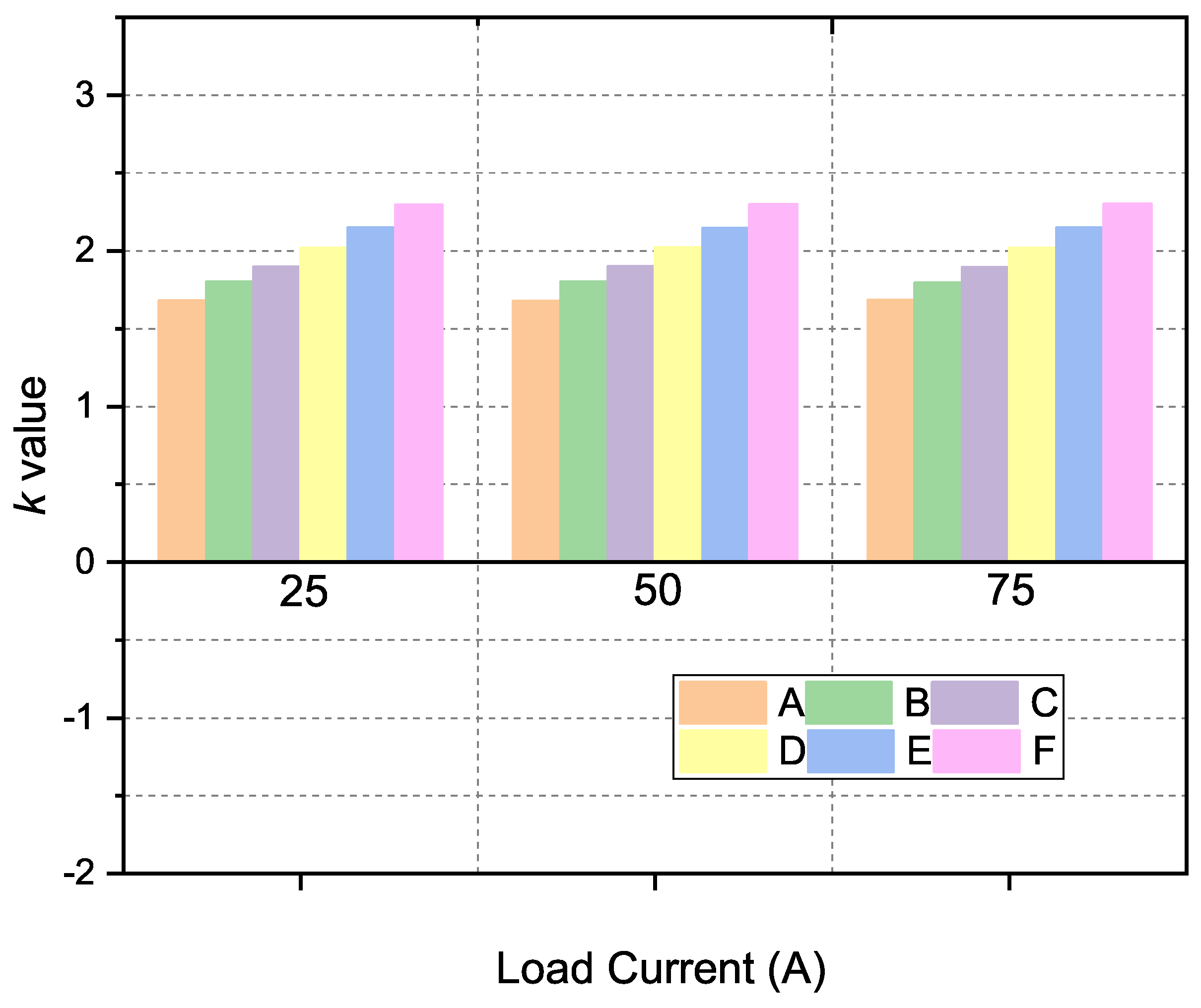
Firstly, the effectiveness of
k as an indicator of solder fatigue is demonstrated. The load currents are applied into the six aging devices. The case temperatures during the various currents for the six aging devices are collected by the NI data acquisition system, as shown in
Table 3, and are used to calculate the value of
k parameter with (
3), respectively.
The estimated
k value for the six aging devices during various currents are shown in
Figure 9. It can be seen from
Figure 9 that the value of
k increases monotonously with the development of solder fatigue, while keeps constant at the same aging conditions during various load currents. This means that the parameter
k just relies on the conditions of solder fatigue, while is independent of the various operation conditions, and therefore is a good indicator for detecting the changes of solder fatigue. In addition, the junction temperatures for the six aging devices are acquired by the IR camera, and are used to calculate the value of
as follows:
where
is the junction temperature under solder fatigue conditions,
P is the power losses of the device, which is composed of conduction loss and switching loss, and can be estimated according to the work in [
20,
22,
23,
24].
Based on (
8), the values of
for the six aging devices are obtained. Thus, the relationships between
and
k parameter are built, as shown in
Table 4. In practical applications, with the measured
k parameter,
can be obtained according to the look-up table recording the information of
and
k.
Secondly, the effectiveness of the model parameters update during solder fatigue conditions is illustrated. The initial parameters of the electro-thermal model is necessary. The extraction of the model parameters is described in detail in [
19,
20,
22,
23,
24]. According to the work in [
19,
20,
22,
23,
24], the model parameters for the healthy device is acquired, and shown in
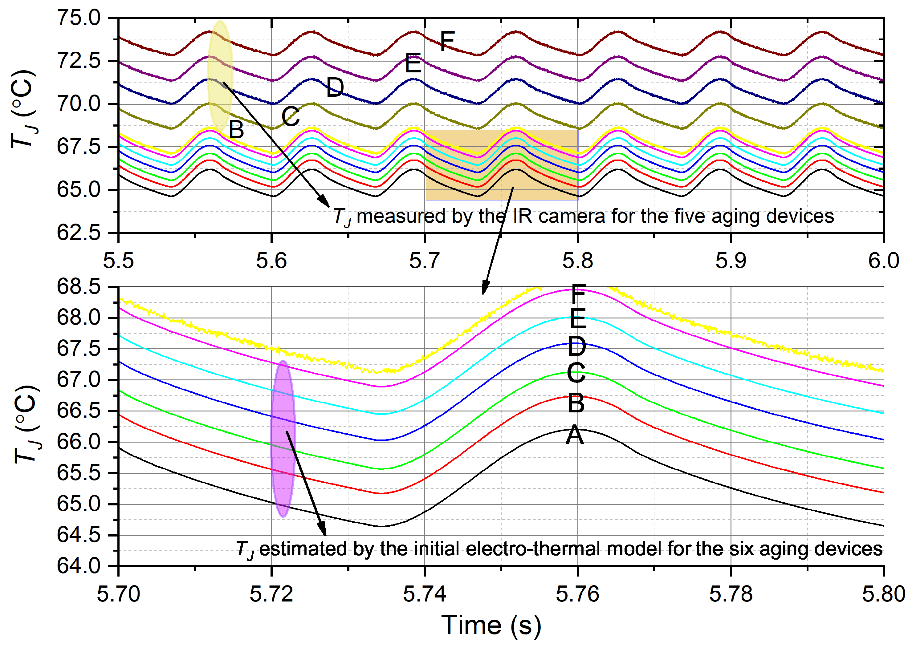
Table 5. To examine the performance of the initial (traditional) electro-thermal model under solder fatigue conditions, the load currents are applied into the six aging devices. The junction temperatures from the initial (traditional) electro-thermal model and the IR camera are obtained and shown in
Figure 10.
It can be seen from
Figure 10 that the junction temperatures of the six aging devices from the initial (traditional) electro-thermal model are increased; this is due to the increase of power losses and
caused by solder fatigue. In addition, with the development of solder fatigue, the temperature difference between the initial (traditional) electro-thermal model and IR camera increases from 0.12 to 5.8
C, meaning that the initial (traditional) electro-thermal model is unable to meet the accuracy requirement of the temperature estimation under solder fatigue conditions. If the use of this electro-thermal model is continued, the fatigue conditions of the device may be over-optimistic estimate, which may lead to catastrophic failure of the device. Thus, the parameters of the electro-thermal model have to be updated to recover the accuracy of the junction temperature estimate.
As discussed in
Section 3, the model parameters can be updated by (
6) and (
7) with the information of
shown in
Table 4. Taking the information of
into (
6) and (
7), the updated parameters of electro-thermal model under solder fatigue condition of F are obtained, and shown in
Table 6.
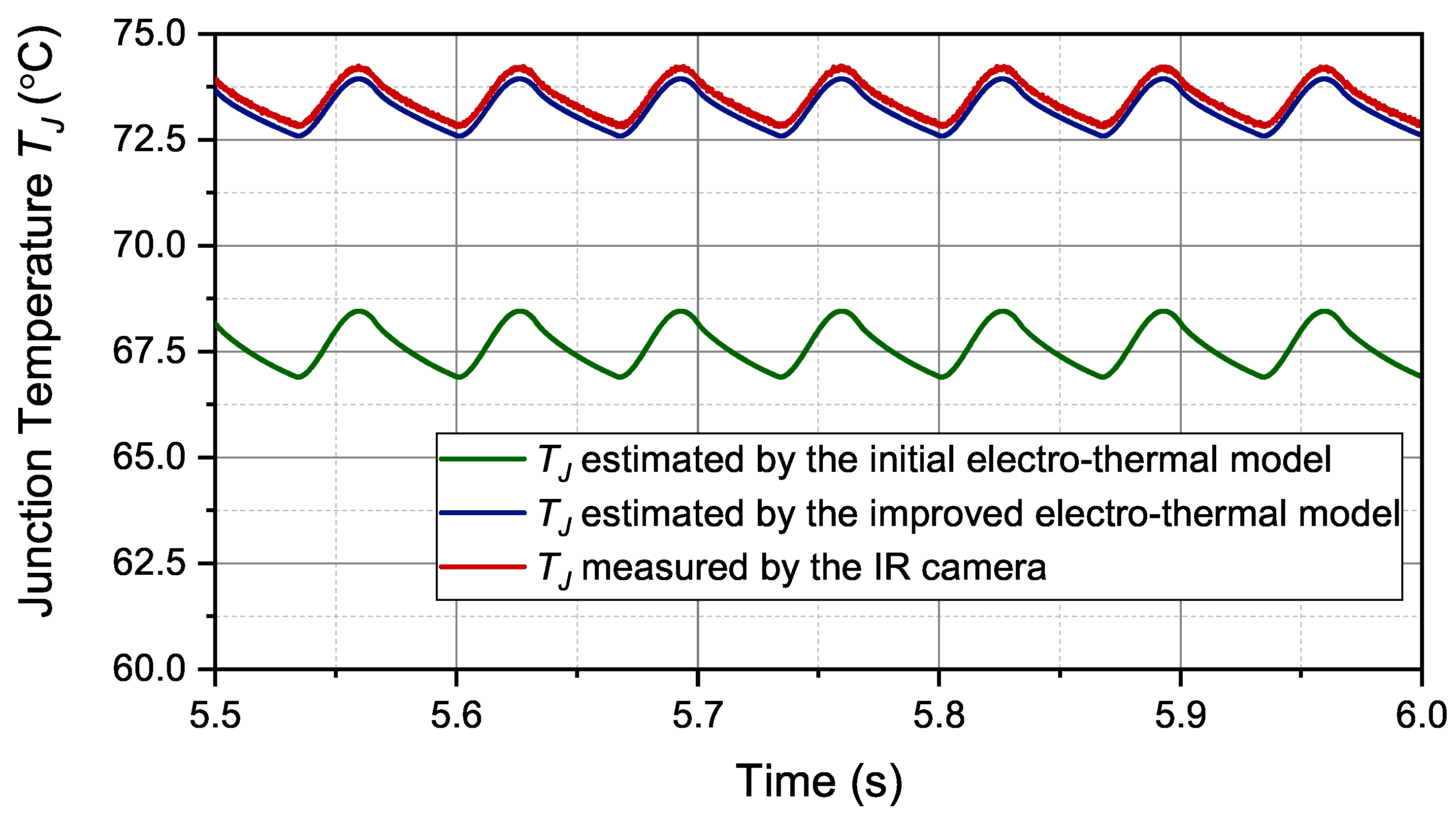
To further demonstrate the performance improvement in temperature estimate accuracy of the improved electro-thermal model, the same sinusoidal currents with 75 A amplitude are applied into the aging device of F, the junction temperatures from the initial (traditional) electro-thermal model, the improved electro-thermal model, and the IR camera are shown in
Figure 11.
Figure 11 shows the junction temperatures
estimated by the initial (traditional) electro-thermal model and the improved electro-thermal model in comparison to the
measurement obtained from IR camera. Obviously, the
estimate by the improved electro-thermal model tracks the
results from IR camera accurately during the various operation conditions with a maximum error of 0.4%. The maximum difference between the two temperature signals is about 0.31
C, which may be linked to the errors inherited from the modeling process, while the temperature difference between the initial (traditional) electro-thermal model and the IR camera exceed 5
C during the operation conditions. The results described above indicate that compared with the initial (traditional) electro-thermal model, the improved electro-thermal model has better performance in temperature estimate accuracy.
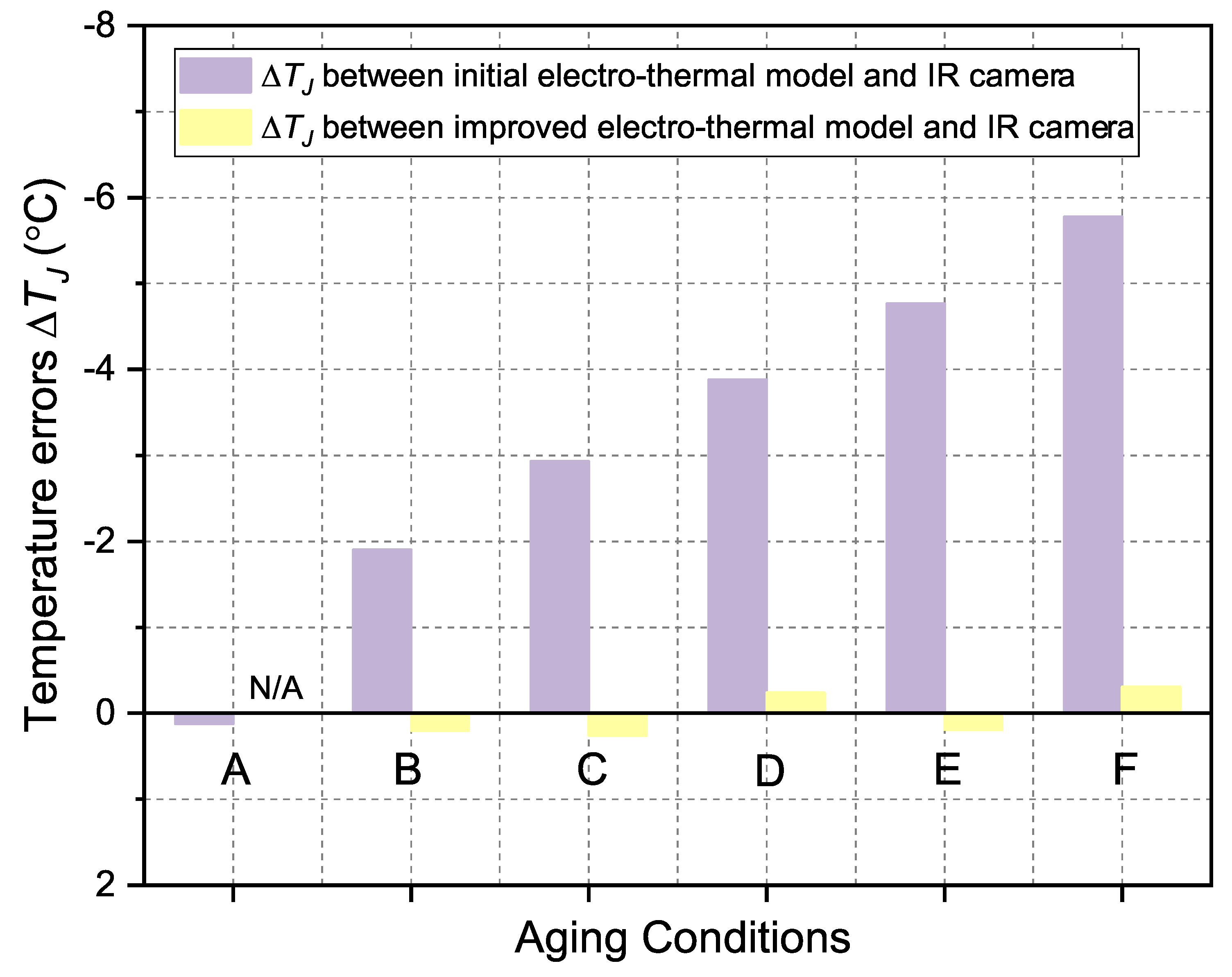
To further examine the effectiveness of the model parameters update, the load currents are applied to the six aging devices. Subtracting the
estimated by the initial (traditional) and improved electro-thermal model from that obtained with the IR camera, the temperature differences between the initial (traditional) and improved electro-thermal model and the IR camera are obtained and shown in
Figure 12.
From
Figure 12, we can see that with the update process, the temperature estimate accuracy of the electro-thermal model improved effectively. The influence of solder fatigue on the temperature estimate by the electro-thermal model has almost been removed. With the proposed method in this paper, the junction temperature of the device can be acquired accurately, which can guarantee the device operates in a reliable mode.


