Article

A Spiking Neural Network Based on the Model of VO2–Neuron

Institute of Physics and Technology, Petrozavodsk State University, 31 Lenina str., Petrozavodsk 185910, Russia
*
Author to whom correspondence should be addressed.
Electronics 2019, 8(10), 1065; https://doi.org/10.3390/electronics8101065
Submission received: 27 August 2019 / Revised: 13 September 2019 / Accepted: 18 September 2019 / Published: 20 September 2019
(This article belongs to the Special Issue Semiconductor Memory Devices for Hardware-Driven Neuromorphic Systems)

Abstract

:
In this paper, we present an electrical circuit of a leaky integrate-and-fire neuron with one VO2 switch, which models the properties of biological neurons. Based on VO2 neurons, a two-layer spiking neural network consisting of nine input and three output neurons is modeled in the SPICE simulator. The network contains excitatory and inhibitory couplings, and implements the winner-takes-all principle in pattern recognition. Using a supervised Spike-Timing-Dependent Plasticity training method and a timing method of information coding, the network was trained to recognize three patterns with dimensions of 3 × 3 pixels. The neural network is able to recognize up to 105 images per second, and has the potential to increase the recognition speed further.

Graphical Abstract

1. Introduction

Artificial neural networks (ANNs), created by analogy with biological neural systems, are used to resolve various tasks, such as classification, clustering, and pattern recognition [1,2,3,4]. The main element of ANN is a neuron that may have several inputs and one output, and neurons can be connected in different ways, depending on the network architecture [5,6]. The main task of a neuron is to convert input signals to output signal using an activation function [5]. In the history of ANN, three generations of the networks are usually distinguished. The first generation includes simple forward and backward connection networks that operate with binary data and stepwise activation functions [7]. The second generation includes multilayer networks of direct and reverse distribution, operating with rational numbers with continuous activation functions [7]. The third generation of ANN (spiking neural networks (SNN)) uses biosimilar models of neurons that take into account not only the magnitude of the signals arriving at the input, but also the signals’ temporal distribution [7,8].
There is a large number of SNNs, which are used to solve practical tasks and are based on mathematical models of neurons (Integrate-and-Fire, Izhikevich, Hodgkin-Huxley) [9,10,11,12]. Such SNNs use the resources of computers, video cards, and field-programmable gate arrays to emulate the network operation [9,10,11,12,13]. Although such SNNs currently provide impressive performance results [14], any emulation loses hardware implementation in performance and energy efficiency [15,16]. Therefore, the development of SNNs based on microelectronic elements attracts the active attention of researchers [16,17,18,19,20,21,22]. One of the most frequently used functional elements of SNN is a memristor [16], which is used for implementing customizable weights and as a functional element of a neuron. The weights are adjusted during the network training, and, in electric networks, it is implemented by changing the impedance of the lines connecting the outputs and inputs of neurons. A multi-stable resistive memory cell is an ideal object for implementing a wide SNN functionality, due to the possibility of changing the resistance over a wide range of values. However, the application of a resistive memory cell as a bi-stable element with an off state (inactive neuron) and on state (active neuron) is not an optimal solution because of the high probability of its resistance modification during the operation [23,24].
In the current study, for the manufacturing of artificial neurons, we propose to use elements with a stable S-shaped I – V characteristic, such as switches based on transition metal oxides with a metal-insulator transition [25,26,27]. Implementations of neuron models on the VO2 switch are described in References [28,29,30,31,32,33,34]. However, a few SNN implementations using such neurons have been proposed so far. Models of VO2 neurons can be divided into two groups. The first group is an integrate-and-fire model of a neuron [32,33,35], which has three main states: the accumulation of action potential state due to charging the capacitor, the spike generation state, when the capacitor is discharged, and the VO2 switch goes into a highly conductive state, and the inactivity state of a neuron. The discharge time of the capacitor is treated as a post firing refractory period [30,32], and the initiation of the second pulse is impossible at that time due to shunting of the low resistance of the switch. The second group of models covers neuron circuits that include inductance, and the possibility of generating a burst mode, which is similar to the FitzHugh-Nagumo and FitzHugh-Rinzel models [34,35].
We propose a leaky integrate-and-fire (LIF) circuit for a neuron based on a VO2 switch that can implement excitatory and inhibitory couplings. Based on VO2 neurons, in the SPICE simulator, the operation of a two-layer SNN network consisting of nine input and three output neurons was modeled. An image in the form of a 3 × 3 matrix is fed to the network input, and, at the output, one of the three neurons is activated with a certain input pattern, and this neuron suppresses the remaining output neurons according to the winner-take-all (WTA) principle [36]. The coding of information in the proposed network is performed by setting the delay time of the spikes in the input layer relative to the zero time moment (time to the first spike) [37]. Network training is performed according to the spike time-dependent plasticity (STDP) scheme [14,16,19,20,21,38]. As a result, a model SNN, based on VO2 neurons, which allows pattern recognition, is presented and investigated in this study.

2. SNN Modeling Method

2.1. VO2 Neuron Model

The VO2-neuron model is created on the basis of the LIF neuron model, which is widely used due to the simplicity of implementation and the possibility of generating biosimilar spikes [39]. Its main element is a bi-stable two-electrode VO2 switch [25,26,27]. The operation principle of the switch is based on the metal-insulator phase transition in VO2 films, which happens near the transition temperature Tth ~ 340 K. The critical temperature Tth in the film is achieved due to the Joule heating effect when passing a current, which leads to a sharp abrupt change in the resistance [27]. In addition to the thermal effect, when modeling electric switching, the effect of the electric field on the concentration of charge carriers is taken into account [40,41]. The model I – V characteristic of the VO2 switch corresponds to the experimental I – V characteristic (Figure 1), measured in our previous work [25], on a planar switch with a channel size of 2.5–3 μm, and a VO2 film thickness of ~ 250 nm, with a current limiting resistor of 250 Ω connected in series.
Figure 1 demonstrates the dependence of the switch current Isw on the voltage Vsw supplied to the switch. Reaching the threshold switching voltages Vth = 5.6 V and holding voltage Vh = 2.2 V, the switch passes from a high-resistance state to a low-resistance state and vice versa. The high-resistance and low-resistance branches of the I – V characteristic are approximated by linear dependencies on the voltage Vsw with resistance values Roff ~ 14 kΩ and Ron ~ 300 Ω, respectively.
To conduct SPICE simulations of the VO2 neuron, a standard voltage-controlled switch was used with parameters corresponding to the experimental I – V characteristics (Roff, Ron, Vth, and Vh).
The electrical circuit of the VO2 neuron is shown in Figure 2. The neuron model has n inputs, and one output Vout. Resistances R w 1 R w n play the role of a synaptic weights between neurons. The smaller the resistance, the more the signal from the i-th input affects the neuron. The spikes coming from the inputs through the resistances are accumulated on the Csum capacitance, by charging it with the cumulative charge. The charge from the Csum capacitor gradually flows through the resistance Rin. Csum capacitance voltage is an effective input signal that affects the current state of a neuron. The supply voltage Vdd is selected so that the VO2 switch stays in the off state in the absence of input signals. The most clear way to achieve this condition is to set the voltage Vdd less than the switching voltage Vth. In this model, the inactive state of the neuron corresponds to the switched off VO2 switch when it is in the subthreshold mode (Vsw <Vth). To activate the neuron, the switch should be turned on by setting the voltage on the switch to VswVth. To achieve this, the supply voltage Vdd must have negative values, and the spikes supplied to the input must have a positive polarity.
To activate a neuron, the voltage across the capacitance Csum should increase to a threshold value Vc_th, which depends on Vdd, the resistance of the switch in the off state Roff, and the values of the resistors Rs and Rin. After the switch is turned on, its resistance decreases to Ron, which leads to the discharge of the capacitance Cc through the resistances Rin and Rout. The capacitance Cc serves as a reservoir of charge, which is necessary for generating a spike when a neuron is activated. When Cc is discharged, a spike of positive polarity is generated at the output Vout of the neuron. By connecting the outputs of some neurons with the inputs of other neurons, SNNs with excitatory coupling can be obtained. The resistance Rs is load resistance and sets the operating current through the switch. Rs is selected in a way that the VO2 switch turns off after discharging the capacitance Cc. In fact, the neuron circuit is tuned to generate a single current spike through the VO2 switch, i.e., generate a single spike at the output.
Figure 3a presents the electrical circuit of a VO2 neuron. The pulses from the voltage generator are supplied to the input of the neuron, and the output is connected to the input stage of the subsequent neuron (to simulate the output load of the neuron). The circuit modeling was performed in the LTspice XVII simulation software. Resistance and capacitance values: Rw_1 = 500 Ω, Rw_2 = 1 kΩ, Rs = 700 Ω, Rin = 1 kΩ, Rout = 10 kΩ, Csum = 1 nF, and Cc = 10 nF. Supply voltage Vdd = −5.75 V. A pulse of positive polarity with an amplitude of 2 V and a duration of 0.3 μs is supplied from the generator. Figure 3b depicts the oscillograms of the input Vin and output Vout voltages, as well as the voltages Vc at the capacitance Csum, which demonstrates the spikes’ dynamics.
The threshold voltage at the Csum capacitance, required to initiate the output spike, is Vc_th ~ 0.33 V (dashed line in Figure 3b). After turning on the VO2 switch, the capacitance Cc starts to discharge, and it leads to the appearance of a leading edge and a spike with a voltage amplitude of ~ 3.2 V. After turning on the switch, a decrease in the voltage Vc to negative values is associated with active recharging of the Csum capacitor through an open switch due to the negative voltage on Cc capacity and Vdd power supply. The spike duration is ~ 170 ns, which is determined by the discharge time of the capacitance Cc until the moment, when the voltage at the switch Vsw is not less than Vh. The trailing edge of the pulse appears when the switch goes off. The duration of the output spike can be significantly longer than the duration of the initiating pulse.
The VO2-neuron model is able to demonstrate various properties of real neurons, such as spike latency, subthreshold oscillations, refractory period, threshold behavior, and spike frequency adaptation [28,39].
For example, Figure 4a demonstrates that the higher the amplitude of the input pulse exists, the smaller the time delay between the leading edges of the input and output pulses remains, called spike latency. With a pulse amplitude of 2 V, the latency between the input and output signals is 140 ns, and with a pulse amplitude of 1 V, the latency reaches 440 ns. Therefore, the amplitude and duration of the input pulse, required to initiate the spike, can lie in a wide range. However, when the amplitude of the input pulse is less than Vc_th, the initiation of the output pulse does not occur.
If the input pulse is sufficiently long, several spikes can be obtained at the output of the circuit. Figure 4b demonstrates the response of a VO2 neuron to a pulse with an amplitude of 1 V and a duration of 3.6 μs, which forms five spikes at the output. The latter mode resembles the occurrence of oscillations when an excitation signal is applied (subthreshold oscillations). The delay between the spikes Tr, called the refractory period, is approximately 630 ns and is determined by the charging time of the capacitor Csum to voltage Vc_th. The refractory period depends on the amplitude of the pulse. For example, at a pulse amplitude of 2 V, the period Tr is 300 ns. In addition, the refractory period Tr is slightly increasing (see the values indicated in Figure 4b), because of the small increase in Vc_th from spike to spike, since the capacitance Cc does not have time to charge to its original values. This increase in the time period between the spikes under constant exposure is similar to biological neurons (spike frequency adaptation) [28,39].
If the delay between the spikes is less than the refractory period, the neuron generates only one spike. Figure 4c demonstrates two input pulses with an amplitude of 1 V and a delay of 300 ns, and the neuron generates a spike only for the first input pulse.
To implement the wide functionality of neural networks, in addition to excitation connections, the possibility to add inhibitory connections is required. Inhibitory connections are widely used in the SNN output layer to implement the WTA rule. Such connections allow the first spike-generated neuron to deactivate all other related neurons using the inhibitory connections. As a result, only one neuron, which is associated with a recognized class, is activated. Figure 5a demonstrates a diagram of two neurons interconnected via capacitances Cinh = 10 nF, which act as inhibitory connections. The capacitance and resistance values correspond to the single neuron circuit shown in Figure 3a, with the exception of Rin = 200 Ω and Rout = 200 Ω. Due to the presence of Cinh capacities, upon activation of one of the neurons and the discharge of its capacitance Cc, the voltage on the capacitance Cc of an inactive neuron decreases. In this case, the first (in time) activated neuron will suppress all other neurons connected to it by inhibitory connections. Namely, in such a group of neurons, the WTA rule is implemented. In order to trace the activation of neurons in this circuit, it is convenient to monitor the current Isw and voltage Vsw on two switches (Figure 5b). The delay between the supplied pulses Vin_1 and Vin_2 is 2 μs. When the first pulse Vin_1 arrives at the first switch (Figure 5b), the switch turns on, the current Isw_1 increases sharply, and the on mode lasts for ~ 4.2 μs. Switching on occurs because the voltage Vsw_1 reaches the threshold value Vth (Figure 5b). After turning on the first switch, the voltage Vsw_1 drops sharply and it leads to a decrease in voltage Vsw_2 on the second switch, as the signal is transmitted through the capacitors Cinh. The second pulse arriving at the input of the second neuron (Vin_2) does not activate it, because the voltage Vsw_2 does not reach the threshold value (Vsw_2 <Vth). The activation of the first neuron inhibits the activation of the second neuron. If an excitation pulse is applied to the second neuron after deactivation of the first neuron, then the second neuron will go into an active mode.
To determine the activity of neurons in the output layer, the most appropriate solution would be to convert the Isw current pulses into output voltage pulses. However, this solution requires additional external circuits. As neurons are connected by Cinh capacities, voltages, taken from Rout resistors, are correlated, and it is not advisable to use them. Schematically, as activity markers, the voltages Vc_1 and Vc_2 can be used, and their dynamics are shown in Figure 5c. When the first neuron is activated, the voltage Vc_1 drops sharply due to the recharging of the capacitor Csum, which forms a strong pulse of negative polarity, and the positive pulse Vc_2 is weakly expressed on the inactive neuron.

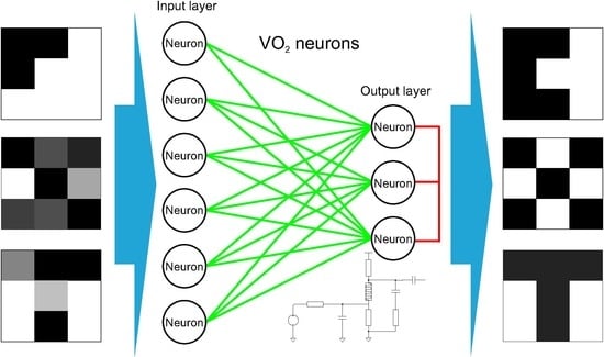
2.2. SNN Architecture

For pattern recognition problems, various SNN architectures are used, which differ in the number of layers and in the way neurons are connected [14,16]. One of the simplest SNN architectures is a two-layer network (Figure 6a), where image information is supplied to the input (first layer), and one of the neurons associated with a certain class of images is activated at the output (second layer) [42,43,44]. Each of the first layer neurons is connected to each neuron of the second layer through excitatory connections. The connection strength between each pair of neurons is specified through synaptic weights, which can vary among themselves. All neurons of the output layer are interconnected by inhibitory connections. When applying signals to the first layer neurons, they are activated and transmit an excitation effect to the second layer. The neuron of the output layer, which is activated first, sends an inhibitory signal on all other output neurons. This prevents their activation. In this way, the WTA rule is implemented, when data is classified by defining the only active neuron in the output layer. The activation speed of the output layer neurons depends on the input signals and synaptic weights between the particular output neuron and each neuron from the input layer. For the correct pattern recognition, during the network training, it is necessary to correctly set the synaptic weights for each group of the output neuron on the input neurons.
Figure 6b presents a coupling diagram of neurons of the input and output layers of a pulsed neural network for image classification. Each element of the input layer corresponds to one pixel of the image. Therefore, to solve the problem of classifying images with a size of 3 × 3 pixels, nine neurons in the input layer are required. The number of output neurons depends on the number of patterns that the network is supposed to recognize. In this study, we will demonstrate the classification of images using three patterns, so the number of neurons in the output layer will be three. The input and output layers of the SNN are connected using synaptic weights, implemented through the resistances Rw_i, j, where i is the number of the input neuron and j is the number of the output neuron. The resistance values Rw_i, j will change during training. Memristors [16], where resistance can be adjusted, are often used as resistances in the circuits. In this study, we do not consider a circuit implementation that allows the change of resistances Rw_i, j during the training process. Instead, we assume to have control over the elements’ resistances. The range of resistance values Rw_i, j varies from 1.5 kΩ to 2.5 kΩ.
A signal from the generator, which encodes information about the color of the pixel, is supplied to the input of each input layer neuron. In this study, we use eight-bit grayscale images, so the information encoded by the generator reflects a gray scale, where the black pixel corresponds to the number 0 and the white pixel corresponds to the number 255. The generator is connected to the input layer neuron using an excitation connection. Then, all nine neurons of the input layer are connected by excitation connections to the three neurons of the output layer, which forms 9 × 3 = 27 connections.
All output neurons are interconnected by inhibitory connections, which are implemented by connecting to the inhibitory bus using the capacitance Cinh = 10 nF.
The remaining elements, depicted in Figure 6b, have the following ratings: Rw = 500 Ω, Rs = 700 Ω, Rin_i = 1 kΩ, Rin_j = 200 Ω, Rout_i = 10 kΩ, Rout_j = 200 Ω, Csum = 1 nF, and Cc = 10 nF. The supply voltage of all neurons is Vdd = −5.75 V.

2.3. SNN Training

Before considering the network training algorithm, it is necessary to determine the method of information coding. A large number of information coding methods for SNN has been defined: rate coding, rank coding, time to first spike, latency coding, phase coding, population coding, and others [37]. Typically, two-layer neural networks, used to classify images, apply the rate coding method [43,45,46]. However, in the current study, we use the time to the first spike method [37]. This coding method requires fewer spikes for a single recognition act, and, as a result, less energy is spent on the circuit operation, as most of the energy is spent on generating spikes.
The information coding is performed as follows. The signals from the generators arrive on the first layer of the neural network with a delay Δt relative to the start time of the circuit t = 0, and the delay Δt determines the brightness of the image pixel. The value Δt = 0 corresponds to brightness 0 (black color), and the maximum delay Δtmax = 2 μs corresponds to brightness 255 (white color). The signal from the generator is a rectangular pulse with an amplitude of 2 V and a duration of 0.3 μs. The delay time is counted relative to the leading edge of the pulse.
The network training process is based on the standard STDP mechanism [14,16,19,20,21,38]. This mechanism is an implementation of the Hebbian learning rule and causes a change in synaptic weight depending on the delay Δtin-out between pre-synaptic and post-synaptic spikes [45]. The traditional rule is an exponential function [45], which depends on Δtin-out. However, various studies use the simplified versions [42,47], which significantly facilitate the calculations, while maintain the main ideas of the SPDT method. In this study, we use the function presented in Figure 7, where the form is given in the SNN training papers [42,45,47]. Since an increase in synaptic weight corresponds to a decrease in resistance Rw_i, j, the function is inverted in relation to the axes of an ordinate. Resistance decreases, if the post-synaptic spike (from the neuron in the output layer) arrives with a delay in the range of 0 to 0.5 μs after the pre-synaptic spike (from the neuron in the input layer). In other cases, the resistance Rw_i, j increases.
Typically, the STDP-based training procedure is used in SNN with unsupervised learning [19,20,21,42,44]. In this case, when training input data is supplied, the output neurons are randomly associated with input data patterns. Nevertheless, there are studies on SNN training mechanisms that implement supervised learning [48,49,50]. In these studies, the input pattern is forcibly assigned to a specific output neuron using back error propagation algorithms. In our study, we tried to implement a simplified approach that allows us to implement supervised learning. During the training, the supply voltage Vdd was set to be non-zero only at one of the three output neurons (see Table 1). The remaining neurons are forcibly electrically deactivated. They do not emit spikes, and it causes all the associated weights Rw_i, j to increase. During network training (Table 1), power at the output neuron No. 1 is present (Vdd ≠ 0) only when “Pattern 1” images are inputted. When “Pattern 2” and “Pattern 3” images are supplied, the voltage Vdd is zero.
The SNN training algorithm consists of the steps listed in Figure 8. First, arbitrary resistances Rw_i, j are set in the range from 1.5 kΩ to 2.5 kΩ. Second, the iterative process of changing the resistances Rw_i, j begins. Initially, one of the patterns, that the network should be trained to express, is arbitrarily selected (the number of patterns should be equal to the number of the output layer neurons). In accordance with the pattern and the information coding scheme, the pulse delays are set to be supplied from the generators to the input layer neurons. Then, in accordance with Table 1, the Vdd values of the output neurons are set. Next, the circuit modelling starts in the SPICE simulator. Based on the simulation results, delays between pre-synaptic and post-synaptic spikes Δtin-out are calculated, and ΔRw_i, j are calculated using the resistance change function (Figure 7). After that, the new values of Rw_i, j are set, and, if the values are outside the range of 1.5 kΩ – 2.5 kΩ, Rw_i, j is set equal to the nearest border value. The training cycle is repeated, until all the Rw_i, j values stop changing.

3. Results

Three patterns for training with a dimension of 3 × 3 pixels are presented in Figure 9. The patterns have the same number of black and white pixels. If the number of black pixels is different, then normalization by color intensity can be applied to obtain more accurate results [51].
Figure 10 illustrates the resistance values Rw_i, 1, Rw_i, 2, and Rw_i, 3 between all input neurons and three output neurons before and after network training. Resistance values are grouped by nine pieces according to the number of output neurons.
Before training, the resistances Rw_i, j were randomly generated in the range from 1.5 kΩ to 2.5 kΩ. Then, the SNN training procedure was performed for ~100 cycles, described in detail in Chapter 2.3, using the input patterns in Figure 9. As a result, the distribution of resistances for each output neuron began to correspond to the pattern assigned to each output neuron. This distribution is an expected result for two-layer networks operating, according to the WTA mechanism [44]. If the training patterns were a set of images distributed by classes (for example, numbers written in different handwriting), then the distribution of weights would be averaging all patterns belonging to the same class. Such a training outcome is observed in the studies using the MNIST database [42].
Analysis of the trained network reveals the following results. If patterns from the training set were input, then, as expected, the neurons corresponding to the associated pattern were activated at the SNN output.
Furthermore, images corresponding to distorted patterns in which pixel color intensities were randomly changed were inputted. The results of the SNN operation with the number of the activated output neuron are presented in Figure 11. The first three images corresponding to the distorted patterns from the training set were correctly classified by SNN. The first image corresponds to “Pattern 3,” the second image corresponds to “Pattern 1,” and the third image corresponds to “Pattern 2.”
When inputting the fourth image, which is a highly distorted template from the training set (“Pattern 3”), none of the output neurons were activated, and it could be interpreted as an undefined result. Inactivity of the output neurons reflects that the voltage on the capacitors Csum of the output neurons never reaches the threshold values Vc < Vc_th.
This uncertainty could be avoided by reducing the time range for spikes coding Δtmax (see Section 2.3). For example, if Δtmax = 2 μs is reduced by half to Δtmax = 1 μs, then the fourth image in Figure 11 is correctly identified as “Pattern 3.” The pulses have shorter time intervals, and the voltage on the integrating capacitance Csum is more likely to increase to the threshold value Vc_th.

4. Discussion

When modelling neurons, on the one hand, we could strive for greater bio-similarity of a neuron, as implemented in some models (FitzHugh-Nagumo, Izhikevich, Hodgkin-Huxley) [35,39], or, on the other hand, we could try to minimize the number of electrical components in the circuit to contribute to its miniaturization in practical implementation. The integrate-and-fire neuron model, which we propose, permits, on the one hand, to obtain a number of properties observed in biological systems (Section 2.1), and, on the other hand, it contains only one switching element and a power source, in contrast to more complex models [28]. In a number of studies of neurons based on VO2, silicon semiconductor devices (field effect transistor, diode) are used as additional circuit elements [22,29]. This imposes certain restrictions on the compatibility of technological processes for manufacturing the silicon and non-silicon parts of the circuit. This drawback is avoided in the presented neuron model, where all circuit elements (switch, resistors, and capacitors) are manufactured using vanadium oxides of various stoichiometry (VO, VO2, V2O3, and V2O5).
All the results presented in the current study were obtained by modeling the VO2 neuron using numerical methods in the LTspice simulator. However, the I–V characteristic of the VO2 switch corresponding to the experimental data was used in the model (see Section 2.1). Therefore, a discussion of the physical mechanisms that affect the I–V characteristics is of great importance for predicting the areas of practical application and comparing the characteristics of neuron models.
An increase in the ambient temperature T0 leads to a decrease in the threshold voltage Vth, and at T0~ Tth, the effect of electrical switching will be suppressed, because the VO2 channel will achieve a highly conductive state [41,52,53]. It imposes a limitation on the use of a VO2 neuron, where the operability will be limited at T0 > Tth. The value of Tth is not high, and reaches Tth ~ 340 K (67 °C) and creates the question - how to increase Tth? A good overview of the Tth modulation methods by doping with various elements is presented in Reference [54]. For example, Cr doping can increase Tth by 10 °C [55]. An alternative way to increase Tth is to use other materials with an S-type I–V characteristic. NbO2–based structures, having Tth ~ 1070 K, demonstrate electrical switching up to temperatures of T0 ~ 300 °C [56], and can be used in the presented neuron model. The model is invariant to the use of other materials with the effect of electrical switching, and the main requirement is the presence of an S-type I–V characteristic. VO2-based structures are a good model object and are often used in neural circuits. Nevertheless, the task of finding switching structures with a wide temperature range is a promising endeavour.
Another problem is the variation of Vth with the temperature. Therefore, if it is necessary to stabilize the operation of a neuron, it is necessary to come up with additional thermal compensation schemes.
To optimize the circuit presented in Figure 2, we propose to exclude the capacitor Csum from the circuit. When switching a VO2 switch by rectangular pulses, there is an effect of a time delay of switching on the switch. An inverse dependence of the time delay on the pulse amplitude is associated with the thermal heating of the switching channel to the phase transition temperature of the metal insulator. The physics of the electrical switching process is described in detail in Reference [27]. If pulse durations and coding time intervals Δtmax are used within the delay times of the switching, the pulse integration effect can be implemented without Csum capacity, and will be caused by the heat accumulation in the region of the switching channel. A similar idea to use heat storage in the switch region to accumulate action in a neuron was proposed in Reference [31]. The role of capacitors in the oscillator circuit is discussed in a number of sources [25,57,58], and the oscillations can be obtained without an integrating capacitor, while being only due to the effects of heat storage. The study of the effect of temperature integration of input pulses could be the subject of future research.
The coupling between the switches in the network can be implemented not only by electrical coupling through resistors Rw_i, j, but, as described in our previous studies, can be organized through the thermal coupling of the switches [59,60]. The development of spike neural networks with thermal coupling could be the subject of further research.
The reduction of SNN classification uncertainty, when applying a highly distorted template (the right image in Figure 11), by reducing the time interval for coding spikes Δtmax, has its own limitations. The current SNN model does not take into account the effect of the turn-on and turn-off delay of the switch described above. For example, the turn-on time of the VO2 switch, using our input signal amplitudes, does not exceed 10 ns [25], while the turn-off time can be much longer (hundreds of nanoseconds). In the time scale of the current SNN model, operating in microsecond intervals, by taking into account the effect of the turn-on delay, does not affect the results of the SNN operation. However, the turn-on and turn-off times can vary significantly, when using other switches, resistors, and resistances. It should be taken into account when designing SNN.
An important characteristic of the network is the pattern recognition time [61]. The SNN architecture, which we propose, provides recognition time of the coding interval order, corresponding to 2–3 μs. After the recognition is completed, the system requires ~ 7–8 μs to reach the initial state, caused by the recharging of the capacities. Therefore, the current SNN is able to recognize up to 105 images per second, and its performance can be increased by reducing the capacitance rating and scaling the VO2 switches [25]. The implemented method of information coding allows the use of single spikes. It does not only reduce the power consumption compared to the networks using rate coding, but minimizes the time to perform one image recognition operation.
At the end of this section, we present a comparison table of neurons with other proposed neuron devices. The neurons in Table 2 are divided into two groups: neurons based on silicon (CMOS) technology and neurons based on VO2 switches. The main parameters of the neurons are the size of the active element and the energy consumption. Although the silicon neurons have an advantage in these parameters, in our study, the spikes duration is of the least importance. Another advantage of the VO2 neuron compared to the CMOS neuron is, apparently, the high noise level of the current channel that leads to the stochastic behavior of the neuron described in References [33,34]. This property allows the network to escape local minima and reach the global minimum of the error surface.
The spike amplitude, power, and energy consumption of the VO2 neuron depend on the threshold switching voltage Vth, if only the energy release on the VO2 switch is taken into account. The main technological parameters affecting the Vth value are the resistivity in the insulator phase ρoff and the contact geometry [25,32]. In Reference [25], we obtained an equation for approximating Vth.
V th = λ ρ o f f ( T th T 0 ) d a β
where d is the thickness of the VO2 film, a is the inter-electrode distance, λ is the heat-transfer coefficient, and β is the exponential coefficient that determines the effective area of the heated zone in the inter-electrode gap (β < 1).
By decreasing the value of a, the structures with reduced Vth can be obtained. Using Equation (1) and the current value when the structure is turned on, estimated as Ion = Vth/Ron (where Ron = ρon/d), we can propose an equation for the maximum power per spike (λ = 35 W/m ∙ K, ρoff = 4 ∙ 10−2 Ω ∙ m, ρon = 4 ∙ 10−4 Ω ∙ m, β = 0.56, Tth = 340 K, T0 = 300 K [25]):
P max = V th I on = λ ρ off ρ on ( T th T 0 ) a 2 β
By reducing the size of the inter-electrode distance a and the ratio (ρoff/ρon), we would significantly reduce the value of Pmax. For example, at a = 1 µm, the maximum power Pmax is ~ 26 mW, while at a = 100 nm, the maximum power Pmax drops to 2 mW.
Espike can be estimated by multiplying the spike duration by the maximum power, Espike~ Pmax⋅Δtspike. In Reference [25], we modelled the switch on and switch off durations of switches, which determine the minimum Δtspike values. We demonstrated that the durations decrease with decreasing a. Therefore, it is possible to predict a significant decrease in Espike with a decrease in the size of switching elements. The estimates are the following: Espike ~ 6.4 nJ at a = 1 μm (Δtspike = 240 ns), and Espike ~ 105 pJ at a = 100 nm (Δtspike = 52 ns).
The last column in Table 2 demonstrates that the majority of the previous studies gives only the model of VO2 neuron itself. In the current study, we present the simple neural network that is capable of pattern recognition, using the timing method of information coding, which has a clear energy advantage over the firing rates coding method [33].

5. Conclusions

In the current study, we present the new model of an LIF neuron based on one switching VO2 element. The neuron circuit was modeled in the LTspice program, and, for the component emulating the switch, a voltage-controlled key was used, which the I – V characteristic corresponded to experimental data. During the simulation, the VO2-neuron model demonstrates biosimilar properties, such as spike latency, subthreshold oscillations, refractory period, threshold behavior, and spike frequency adaptation. A two-layer SNN was designed to allow pattern recognition. The coupling between the neurons of the input and output layers was implemented using excitatory connections, and, inside the output layer, the coupling used inhibitory connections. This architecture led to the activation of only one output neuron associated with the most similar pattern, according to the WTA principle. As an example, we studied the network that had nine input and threeoutput neurons, which was trained to recognize three patterns (3 × 3 pixels). A timing method of information coding was used, where the color intensity of the pixel was determined by the time delay between the spikes. The training was conducted using the supervised SPDT method, taking into account the time delay of pre-synaptic and post-synaptic spikes. To analyze the operation of the trained network, the images of distorted patterns from the training set were sent to the network input, and the images were correctly recognized in most cases. The network is capable of recognizing up to 105 images per second, and the classification process is highly dependent on the time parameters of the network and the effect of electrical switching. Network architecture has the potential for further scaling, which increases the speed of recognition and miniaturization of the components. In the future, we plan to continue the work toward optimization of both the neuron circuit and the network architecture for classifying images from standardized databases [64].

Author Contributions

Conceptualization, M.B. Methodology, M.B. and A.V. Software validation, M.B. Writing—original draft preparation, M.B. and A.V. Project administration, A.V.

Funding

The Russian Science Foundation (grant no. 16-19-00135) supported this research.

Acknowledgments

The authors express their gratitude to Andrei Rikkiev for the valuable comments in the course of the article translation and revision.

Conflicts of Interest

The authors declare no conflict of interest.

References

  1. Min, E.; Guo, X.; Liu, Q.; Zhang, G.; Cui, J.; Long, J. A Survey of Clustering with Deep Learning: From the Perspective of Network Architecture. IEEE Access 2018, 6, 39501–39514. [Google Scholar] [CrossRef]
  2. Cireşan, D.; Meier, U.; Schmidhuber, J. Multi-column deep neural networks for image classification. In Proceedings of the 2012 IEEE Conference on Computer Vision and Pattern Recognition, Providence, RI, USA, 16–21 June 2012; pp. 3642–3649. [Google Scholar]
  3. Abdel-Hamid, O.; Mohamed, A.-R.; Jiang, H.; Deng, L.; Penn, G.; Yu, D. Convolutional Neural Networks for Speech Recognition. IEEE/ACM Trans. Audio Speech Lang. Process. 2014, 22, 1533–1545. [Google Scholar] [CrossRef] [Green Version]
  4. Du, Y.; Wang, W.; Wang, L. Hierarchical recurrent neural network for skeleton based action recognition. In Proceedings of the 2015 IEEE Conference on Computer Vision and Pattern Recognition (CVPR), Boston, MA, USA, 7–12 June 2015; pp. 1110–1118. [Google Scholar]
  5. Patterson, J.; Gibson, A. Deep Learning: A Practitioner’s Approach; O’Reilly: Sebastopol, CA, USA, 2017; ISBN 9781491924570. [Google Scholar]
  6. Liu, W.; Wang, Z.; Liu, X.; Zeng, N.; Liu, Y.; Alsaadi, F.E. A survey of deep neural network architectures and their applications. Neurocomputing 2017, 234, 11–26. [Google Scholar] [CrossRef]
  7. Maass, W. Networks of spiking neurons: The third generation of neural network models. Neural Netw. 1997, 10, 1659–1671. [Google Scholar] [CrossRef]
  8. Ghosh-Dastidar, S.; Adeli, H. spiking neural networks. Int. J. Neural Syst. 2009, 19, 295–308. [Google Scholar] [CrossRef] [PubMed]
  9. Bonabi, S.Y.; Asgharian, H.; Safari, S.; Ahmadabadi, M.N. FPGA implementation of a biological neural network based on the Hodgkin-Huxley neuron model. Front. Mol. Neurosci. 2014, 8, 379. [Google Scholar]
  10. Cheung, K.; Schultz, S.R.; Luk, W. A Large-Scale Spiking Neural Network Accelerator for FPGA Systems; Springer Science and Business Media LLC: Berlin, Germany, 2012; Volume 7552, pp. 113–120. [Google Scholar]
  11. Beyeler, M.; Dutt, N.D.; Krichmar, J.L. Categorization and decision-making in a neurobiologically plausible spiking network using a STDP-like learning rule. Neural Netw. 2013, 48, 109–124. [Google Scholar] [CrossRef] [PubMed]
  12. Diehl, P.U.; Cook, M. Unsupervised learning of digit recognition using spike-timing-dependent plasticity. Front. Comput. Neurosci. 2015, 9, 99. [Google Scholar] [CrossRef] [Green Version]
  13. Beyeler, M.; Oros, N.; Dutt, N.; Krichmar, J.L. A GPU-accelerated cortical neural network model for visually guided robot navigation. Neural Netw. 2015, 72, 75–87. [Google Scholar] [CrossRef] [Green Version]
  14. Tavanaei, A.; Ghodrati, M.; Kheradpisheh, S.R.; Masquelier, T.; Maida, A. Deep learning in spiking neural networks. Neural Netw. 2019, 111, 47–63. [Google Scholar] [CrossRef]
  15. Jeong, D.S.; Kim, K.M.; Kim, S.; Choi, B.J.; Hwang, C.S. Memristors for Energy-Efficient New Computing Paradigms. Adv. Electron. Mater. 2016, 2, 1600090. [Google Scholar] [CrossRef]
  16. Jeong, H.; Shi, L. Memristor devices for neural networks. J. Phys. D Appl. Phys. 2019, 52, 023003. [Google Scholar] [CrossRef]
  17. Srinivasan, G.; Sengupta, A.; Roy, K. Magnetic Tunnel Junction Based Long-Term Short-Term Stochastic Synapse for a Spiking Neural Network with On-Chip STDP Learning. Sci. Rep. 2016, 6, 29545. [Google Scholar] [CrossRef] [PubMed] [Green Version]
  18. Kim, H.; Hwang, S.; Park, J.; Park, B.-G. Silicon synaptic transistor for hardware-based spiking neural network and neuromorphic system. Nanotechnology 2017, 28, 405202. [Google Scholar] [CrossRef] [PubMed]
  19. Wang, Z.; Joshi, S.; Savel’ev, S.; Song, W.; Midya, R.; Li, Y.; Rao, M.; Yan, P.; Asapu, S.; Zhuo, Y.; et al. Fully memristive neural networks for pattern classification with unsupervised learning. Nat. Electron. 2018, 1, 137. [Google Scholar] [CrossRef]
  20. Wang, Z.; Crafton, B.; Gomez, J.; Xu, R.; Luo, A.; Krivokapic, Z.; Martin, L.; Datta, S.; Raychowdhury, A.; Khan, A.I. Experimental Demonstration of Ferroelectric Spiking Neurons for Unsupervised Clustering. In Proceedings of the 2018 IEEE International Electron Devices Meeting (IEDM), San Francisco, CA, USA, 1–5 December 2018; pp. 13.3.1–13.3.4. [Google Scholar]
  21. Zhou, E.; Fang, L.; Yang, B. Memristive Spiking Neural Networks Trained with Unsupervised STDP. Electronics 2018, 7, 396. [Google Scholar] [CrossRef]
  22. Jerry, M.; Tsai, W.-Y.; Xie, B.; Li, X.; Narayanan, V.; Raychowdhury, A.; Datta, S. Phase transition oxide neuron for spiking neural networks. In Proceedings of the 2016 74th Annual Device Research Conference (DRC), Newark, DE, USA, 19–22 June 2016; pp. 1–2. [Google Scholar]
  23. Jeong, D.S.; Thomas, R.; Katiyar, R.S.; Scott, J.F.; Kohlstedt, H.; Petraru, A.; Hwang, C.S. Emerging memories: Resistive switching mechanisms and current status. Rep. Prog. Phys. 2012, 75, 76502. [Google Scholar] [CrossRef]
  24. Li, Y.; Wang, Z.; Midya, R.M.; Xia, Q.; Yang, J.J. Review of memristor devices in neuromorphic computing: Materials sciences and device challenges. J. Phys. D Appl. Phys. 2018, 51, 503002. [Google Scholar] [CrossRef]
  25. Pergament, A.; Velichko, A.; Belyaev, M.; Putrolaynen, V. Electrical switching and oscillations in vanadium dioxide. Phys. B Condens. Matter 2018, 536, 239–248. [Google Scholar] [CrossRef] [Green Version]
  26. Crunteanu, A.; Givernaud, J.; Leroy, J.; Mardivirin, D.; Champeaux, C.; Orlianges, J.-C.; Catherinot, A.; Blondy, P. Voltage- and current-activated metal–insulator transition in VO2 -based electrical switches: A lifetime operation analysis. Sci. Technol. Adv. Mater. 2010, 11, 065002. [Google Scholar] [CrossRef]
  27. Belyaev, M.A.; Boriskov, P.P.; Velichko, A.A.; Pergament, A.L.; Putrolainen, V.V.; Ryabokon’, D.V.; Stefanovich, G.B.; Sysun, V.I.; Khanin, S.D. Switching Channel Development Dynamics in Planar Structures on the Basis of Vanadium Dioxide. Phys. Solid State 2018, 60, 447–456. [Google Scholar] [CrossRef]
  28. Yi, W.; Tsang, K.K.; Lam, S.K.; Bai, X.; Crowell, J.A.; Flores, E.A. Biological plausibility and stochasticity in scalable VO2 active memristor neurons. Nat. Commun. 2018, 9, 4661. [Google Scholar] [CrossRef] [PubMed]
  29. Ignatov, M.; Ziegler, M.; Hansen, M.; Petraru, A.; Kohlstedt, H. A memristive spiking neuron with firing rate coding. Front. Mol. Neurosci. 2015, 9, 49. [Google Scholar] [CrossRef] [PubMed]
  30. Lin, J.; Guha, S.; Ramanathan, S. Vanadium Dioxide Circuits Emulate Neurological Disorders. Front. Mol. Neurosci. 2018, 12, 856. [Google Scholar] [CrossRef] [PubMed] [Green Version]
  31. Amer, S.; Hasan, M.S.; Adnan, M.M.; Rose, G.S. SPICE Modeling of Insulator Metal Transition: Model of the Critical Temperature. IEEE J. Electron Devices Soc. 2019, 7, 18–25. [Google Scholar] [CrossRef]
  32. Lin, J.; Sonde, S.; Chen, C.; Stan, L.; Achari, K.V.L.V.; Ramanathan, S.; Guha, S. Low-voltage artificial neuron using feedback engineered insulator-to-metal-transition devices. In Proceedings of the 2016 IEEE International Electron Devices Meeting (IEDM), San Francisco, CA, USA, 3–7 December 2016; p. 35. [Google Scholar]
  33. Jerry, M.; Parihar, A.; Grisafe, B.; Raychowdhury, A.; Datta, S. Ultra-low power probabilistic IMT neurons for stochastic sampling machines. In Proceedings of the 2017 Symposium on VLSI Technology, Kyoto, Japan, 5–8 June 2017; pp. T186–T187. [Google Scholar]
  34. Parihar, A.; Jerry, M.; Datta, S.; Raychowdhury, A. Stochastic IMT (Insulator-Metal-Transition) Neurons: An Interplay of Thermal and Threshold Noise at Bifurcation. Front. Neurosci. 2018, 12, 210. [Google Scholar] [CrossRef] [PubMed]
  35. Boriskov, P.; Velichko, A. Switch Elements with S-Shaped Current-Voltage Characteristic in Models of Neural Oscillators. Electronics 2019, 8, 922. [Google Scholar] [CrossRef]
  36. Oster, M.; Douglas, R.; Liu, S.-C. Computation with Spikes in a Winner-Take-All Network. Neural Comput. 2009, 21, 2437–2465. [Google Scholar] [CrossRef] [Green Version]
  37. Ponulak, F.; Kasinski, A. Introduction to spiking neural networks: Information processing, learning and applications. Acta Neurobiol. Exp. 2011, 71, 409–433. [Google Scholar]
  38. Serrano-Gotarredona, T.; Masquelier, T.; Prodromakis, T.; Indiveri, G.; Linares-Barranco, B. STDP and STDP variations with memristors for spiking neuromorphic learning systems. Front. Mol. Neurosci. 2013, 7, 2. [Google Scholar] [CrossRef] [Green Version]
  39. Izhikevich, E. Which Model to Use for Cortical Spiking Neurons? IEEE Trans. Neural Netw. 2004, 15, 1063–1070. [Google Scholar] [CrossRef] [PubMed]
  40. Karda, K.; Mouli, C.; Ramanathan, S.; Alam, M.A. A Self-Consistent, Semiclassical Electrothermal Modeling Framework for Mott Devices. IEEE Trans. Electron Devices 2018, 65, 1672–1678. [Google Scholar] [CrossRef]
  41. Pergament, A.; Boriskov, P.; Velichko, A.; Kuldin, N.; Velichko, A. Switching effect and the metal–insulator transition in electric field. J. Phys. Chem. Solids 2010, 71, 874–879. [Google Scholar] [CrossRef]
  42. Querlioz, D.; Bichler, O.; Dollfus, P.; Gamrat, C. Immunity to Device Variations in a Spiking Neural Network with Memristive Nanodevices. IEEE Trans. Nanotechnol. 2013, 12, 288–295. [Google Scholar] [CrossRef]
  43. Shukla, A.; Kumar, V.; Ganguly, U. A software-equivalent SNN hardware using RRAM-array for asynchronous real-time learning. In Proceedings of the 2017 International Joint Conference on Neural Networks (IJCNN), Anchorage, AK, USA, 14–19 May 2017; pp. 4657–4664. [Google Scholar]
  44. Kwon, M.-W.; Baek, M.-H.; Hwang, S.; Kim, S.; Park, B.-G. Spiking Neural Networks with Unsupervised Learning Based on STDP Using Resistive Synaptic Devices and Analog CMOS Neuron Circuit. J. Nanosci. Nanotechnol. 2018, 18, 6588–6592. [Google Scholar] [CrossRef] [PubMed] [Green Version]
  45. Yousefzadeh, A.; Stromatias, E.; Soto, M.; Serrano-Gotarredona, T.; Linares-Barranco, B. On Practical Issues for Stochastic STDP Hardware With 1-bit Synaptic Weights. Front. Mol. Neurosci. 2018, 12, 665. [Google Scholar] [CrossRef] [PubMed] [Green Version]
  46. Saunders, D.J.; Siegelmann, H.T.; Kozma, R.; Ruszinkao, M. STDP Learning of Image Patches with Convolutional Spiking Neural Networks. In Proceedings of the 2018 International Joint Conference on Neural Networks (IJCNN), Rio de Janeiro, Brazil, 8–13 July 2018; pp. 1–7. [Google Scholar]
  47. Bichler, O.; Querlioz, D.; Thorpe, S.J.; Bourgoin, J.-P.; Gamrat, C. Extraction of temporally correlated features from dynamic vision sensors with spike-timing-dependent plasticity. Neural Netw. 2012, 32, 339–348. [Google Scholar] [CrossRef] [PubMed]
  48. Tavanaei, A.; Maida, A. BP-STDP: Approximating backpropagation using spike timing dependent plasticity. Neurocomputing 2019, 330, 39–47. [Google Scholar] [CrossRef]
  49. Nishitani, Y.; Kaneko, Y.; Ueda, M. Supervised Learning Using Spike-Timing-Dependent Plasticity of Memristive Synapses. IEEE Trans. Neural Netw. Learn. Syst. 2015, 26, 2999–3008. [Google Scholar] [CrossRef] [PubMed] [Green Version]
  50. Lee, C.; Panda, P.; Srinivasan, G.; Roy, K. Training Deep Spiking Convolutional Neural Networks With STDP-Based Unsupervised Pre-training Followed by Supervised Fine-Tuning. Front. Mol. Neurosci. 2018, 12, 435. [Google Scholar] [CrossRef]
  51. Garcia, C.; Delakis, M. Convolutional face finder: A neural architecture for fast and robust face detection. IEEE Trans. Pattern Anal. Mach. Intell. 2004, 26, 1408–1423. [Google Scholar] [CrossRef] [PubMed]
  52. Kim, S.; Lin, C.-Y.; Kim, M.-H.; Kim, T.-H.; Kim, H.; Chen, Y.-C.; Chang, Y.-F.; Park, B.-G. Dual Functions of V/SiOx/AlOy/p++Si Device as Selector and Memory. Nanoscale Res. Lett. 2018, 13, 252. [Google Scholar] [CrossRef] [PubMed]
  53. Lin, C.-Y.; Chen, P.-H.; Chang, T.-C.; Chang, K.-C.; Zhang, S.-D.; Tsai, T.-M.; Pan, C.-H.; Chen, M.-C.; Su, Y.-T.; Tseng, Y.-T.; et al. Attaining resistive switching characteristics and selector properties by varying forming polarities in a single HfO2-based RRAM device with a vanadium electrode. Nanoscale 2017, 9, 8586–8590. [Google Scholar] [CrossRef] [PubMed]
  54. Sun, C.; Yan, L.; Yue, B.; Liu, H.; Gao, Y. The modulation of metal–insulator transition temperature of vanadium dioxide: A density functional theory study. J. Mater. Chem. C 2014, 2, 9283–9293. [Google Scholar] [CrossRef]
  55. Brown, B.L.; Nordquist, C.D.; Jordan, T.S.; Wolfley, S.L.; Leonhardt, D.; Edney, C.; Custer, J.A.; Lee, M.; Clem, P.G. Electrical and optical characterization of the metal-insulator transition temperature in Cr-doped VO2 thin films. J. Appl. Phys. 2013, 113, 173704. [Google Scholar] [CrossRef]
  56. Pergament, A.; Stefanovich, G.; Malinenko, V.; Velichko, A. Electrical Switching in Thin Film Structures Based on Transition Metal Oxides. Adv. Condens. Matter Phys. 2015, 2015, 654840. [Google Scholar] [CrossRef]
  57. Lepage, D.; Chaker, M. Thermodynamics of self-oscillations in VO2 for spiking solid-state neurons. AIP Adv. 2017, 7, 055203. [Google Scholar] [CrossRef]
  58. Sakai, J. High-efficiency voltage oscillation in VO2 planer-type junctions with infinite negative differential resistance. J. Appl. Phys. 2008, 103, 103708. [Google Scholar] [CrossRef]
  59. Velichko, A.; Belyaev, M.; Putrolaynen, V.; Perminov, V.; Pergament, A. Thermal coupling and effect of subharmonic synchronization in a system of two VO2 based oscillators. Solid-State Electron. 2018, 141, 40–49. [Google Scholar] [CrossRef]
  60. Velichko, A.; Belyaev, M.; Putrolaynen, V.; Perminov, V.; Pergament, A. Modeling of thermal coupling in VO2 -based oscillatory neural networks. Solid-State Electron. 2018, 139, 8–14. [Google Scholar] [CrossRef]
  61. Savchenko, A. Sequential three-way decisions in multi-category image recognition with deep features based on distance factor. Inf. Sci. 2019, 489, 18–36. [Google Scholar] [CrossRef]
  62. Cruz-Albrecht, J.M.; Yung, M.W.; Srinivasa, N. Energy-Efficient Neuron, Synapse and STDP Integrated Circuits. IEEE Trans. Biomed. Circuits Syst. 2012, 6, 246–256. [Google Scholar] [CrossRef] [PubMed]
  63. Sourikopoulos, I.; Hedayat, S.; Loyez, C.; Danneville, F.; Hoel, V.; Mercier, E.; Cappy, A. A 4-fJ/Spike Artificial Neuron in 65 nm CMOS Technology. Front. Mol. Neurosci. 2017, 11, 1597. [Google Scholar] [CrossRef] [PubMed]
  64. LeCun, Y.; Cortes, C.; Burges, C. MNIST Handwritten Digit Database. Available online: http://yann.lecun.com/exdb/mnist/ (accessed on 9 November 2018).
Figure 1. Experimental I–V characteristic of a planar VO2 switch.
Electronics 08 01065 g001
Figure 2. Electrical circuit of a VO2 neuron.
Electronics 08 01065 g002
Figure 3. (a) An example of an electrical circuit of a VO2 neuron activated by a voltage generator, and (b) oscillograms of voltages Vin, Vout, and Vc illustrating the spikes’ dynamics.
Electronics 08 01065 g003aElectronics 08 01065 g003b
Figure 4. (a) Oscillograms of Vin, Vc, and Vout, applying to the VO2-neuron input pulses of different duration and amplitude, (b) one long pulse, and (c) two pulses with a small delay between them.
Electronics 08 01065 g004
Figure 5. (a) Connection diagram of two oscillators with inhibitory connections. (b) Oscillograms of the input signals Vin_1, Vin_2, voltages Vsw_1, Vsw_2 and currents Isw_1, Isw_2 on the switches, and (c) oscillograms of the input signals Vin_1, Vin_2 and voltages on the integrating capacitors Vc_1, Vc_2, when applying two voltage pulses with a delay of 2 μs.
Electronics 08 01065 g005
Figure 6. (a) Architecture of a two-layer neural network for pattern recognition and (b) circuit implementation of neurons in the input and output layers.
Electronics 08 01065 g006aElectronics 08 01065 g006b
Figure 7. The function of the resistance change the between the input and output neuron ΔRw_i, j depending on the delay between the pre-synaptic and post-synaptic spikes Δtin-out.
Electronics 08 01065 g007
Figure 8. SNN training algorithm.
Electronics 08 01065 g008
Figure 9. Set of patterns used for SNN training.
Electronics 08 01065 g009
Figure 10. Distribution of resistances Rw_i, 1, Rw_i, 2, and Rw_i, 3 before and after training.
Electronics 08 01065 g010
Figure 11. Examples of image classification of distorted patterns indicating activated output neurons.
Electronics 08 01065 g011
Table 1. An example of the supply voltage setting Vdd of the output layer, using the supervised learning method in SNN training.
The Class of the Image, Fed to the SNN InputThe Voltage Vdd of the Output Neuron No. 1, VThe Voltage Vdd of the Output Neuron No. 2, VThe Voltage Vdd of the Output Neuron No. 3, V
Pattern 1−5.7500
Pattern 20−5.750
Pattern 300−5.75
Table 2. Comparison of neurons with other proposed neuron devices.
DeviceNeuron Type Material/Platform Active Element Size (a) and Neuron Area (Sneuron)Spike Amplitude (Vspike), Peak Power (Pmax), Duration, (Δtspike) and Energy per Spike (Espike)Integration and Threshold Mechanism, Threshold Voltage of the Active Element VthSNN with Object Recognition, Coding Mechanism
VO2
(current study)
Leaky Integrate and Fire
Vanadium Dioxide (VO2)
a ~ 3 μmVspike = 3.2 V
Δtspike~500 ns
Pmax~37 mW
Espike~ 18 nJ
Capacitor charging,
Switching effect when reaching Vth,
Vth(VO2)~5.6 V
Time to first spike
Oxide neuron [35]Piecewise linear FitzHugh-Nagumo, FitzHugh–Rinzel
Vanadium Dioxide (VO2),
Niobium oxide (NbO)
a ~ 3 μm
Vspike~3.5V
Δtspike~100 μs
Pmax~72 mW
Espike~ 7 μJ
Capacitor charging and energy of inductance magnetic field,
switching effect when reaching Vth,
Vth(VO2)~ 5.6 V
Vth(NbO2)~ 0.9 V
-
Stochastic VO2 neuron
[33]
Integrate and fire
Vanadium Dioxide (VO2)
a ~ 100 nmVspike~0.5 V
Δtspike~4 μs
Pmax~12 μW
Espike~50 pJ
Capacitor charging,
switching effect when reaching Vth,
Vth(VO2)~ 1.7 V
Rate coding
CMOS neuron [62]Leaky Integrate and fire
CMOS
a ~ 90nm
Sneuron= 442 μm2
Vspike = 0.6 V
Δtspike~3 ms
Espike = 0.4 pJ
Capacitor charging.
Reset using comparator,
Vth~ 0.6 V
-
CMOS neuron [63]Simplified Morris - Lecar model
CMOS
a ~ 65 nm
Sneuron = 35 μm2
Vspike = 112 mV
Δtspike~18 μs
Espike = 4 fJ
Capacitor charging and discharging through transistors,
Vth~ 112mV
-

