Abstract
In this paper we present an oscillating conditioning circuit, operating a capacitance-to-time conversion, which is suitable for the readout of differential capacitive sensors. The simple architecture, based on a multiple-feedbacks structure that avoids ground noise disturbs and system calibrations, employs only three Operational Amplifiers (OAs) and a mixer implementing a square wave oscillator that provides an AC sensor excitation voltage. It performs a Period Modulation (PM) and a Pulse Width Modulation (PWM) of the output signal proportionally to the sensor differential capacitance values. The sensor variation range and the detection sensitivity can be easily set through the additional resistors. Preliminary PSpice simulation results have shown a good agreement with theoretical calculations as well as a linear response with a high detection sensitivity of differential capacitive sensors having a baseline in the range [2.2 ÷ 180 pF]. Moreover, different experimental measurements have been also performed by implementing the circuit on a laboratory breadboard using commercial discrete components so validating the idea and providing the circuit performances with different kind of differential capacitive sensors achieving detection resolutions of about 0.1 fF in an overall differential capacitive variation range that is equal to ±15.8 pF. The achieved results demonstrate that the proposed interface solution is suitable for on-chip integration with different kinds of differential capacitive sensing devices, such as Micro-Electro-Mechanical-System (MEMS), force/position, and humidity sensors in biomedical and robotics applications.
1. Introduction
Recent developments on integration techniques and circuit miniaturizations, together with advances on capacitive sensing technologies, have led to the design of high-sensitivity and small-size devices, like Micro-Electro-Mechanical-System (MEMS), gyroscopes, accelerometers, position/displacement, pressure/force, flow, and humidity sensors having very high detection capabilities that are widely used in robotics/biomedical sensor applications as well as in bioengineering microsystems [1,2,3]. Basically, their behavior can be simply described as a planar capacitor (i.e., C = ε·A/d, being ε the relative dielectric constant, A the active surface, and d the distance between capacitor metal plates) whose mechanical features (i.e., A and/or d) are temporarily changed by the physical phenomena to be detected. Furthermore, in several sensory systems, differential capacitive sensing configurations also provide a suitable reduction of the common-mode noise and the parasitic component effects [4,5,6,7,8,9,10,11,12,13,14,15].
In the literature, capacitive sensor interfaces mainly concern Capacitance-to-Voltage (C-V) and Capacitance-to-Time (C-T) analogue conversion techniques [15,16,17,18,19,20,21,22,23,24]. In particular, the first topology commonly employs voltage/transimpedance amplifiers, charge/chopper amplifiers, and switched capacitors showing limited/reduced detection ranges, sensitivities, and resolutions mainly due to noise issues. On the contrary, the latter approach is typically based on square wave relaxation oscillators in which the sensing operation is performed by the readout of the output signal period (i.e., a Period Modulation, PM) and/or its duty-cycle (i.e., a Pulse Width Modulation, PWM) as a function of the single/differential sensor capacitance. PM-based interfaces are asynchronous and have a measurement time and a resolution generally dependent from the sensor capacitance. On the other hand, PWM-based solutions are synchronous circuit needing a clock line to synchronize the interfacing operation, while their measurement time and resolution are typically independent from the sensor capacitance. These kinds of interface solutions, typically showing straightforward architectures with a high tolerance to common-mode noise/disturbs and to parasitic components as well as to supply voltage drifts, allows for covering wide capacitive variation ranges and can also be combined with a digital system to easily measure the time intervals (e.g., through counters) [25,26,27,28,29,30,31,32,33,34]. Recently, also mixed-signal and digital sensor systems are becoming prevalent, so that new topologies of sensor conditioning circuits have been also introduced. By performing a Capacitance-to-Digital (C-D) conversion (sometimes also combined with C-V or C-T conversions), these architectures can be directly interfaced with a microcontroller even if, sometimes, requiring high frequency clock signals to achieve suitable sensitivities and resolutions [35,36,37,38,39,40,41,42].
However, most of the developed solutions are mainly suitable to only single element capacitive sensors. On the contrary, often direct differential measurements with high acquisition rate, accuracy, precision, sensitivity, and resolution are required, since two single-element measurements could provide errors if not performed simultaneously due to the time variations of the capacitances owed to the occurring dynamic physical phenomenon.
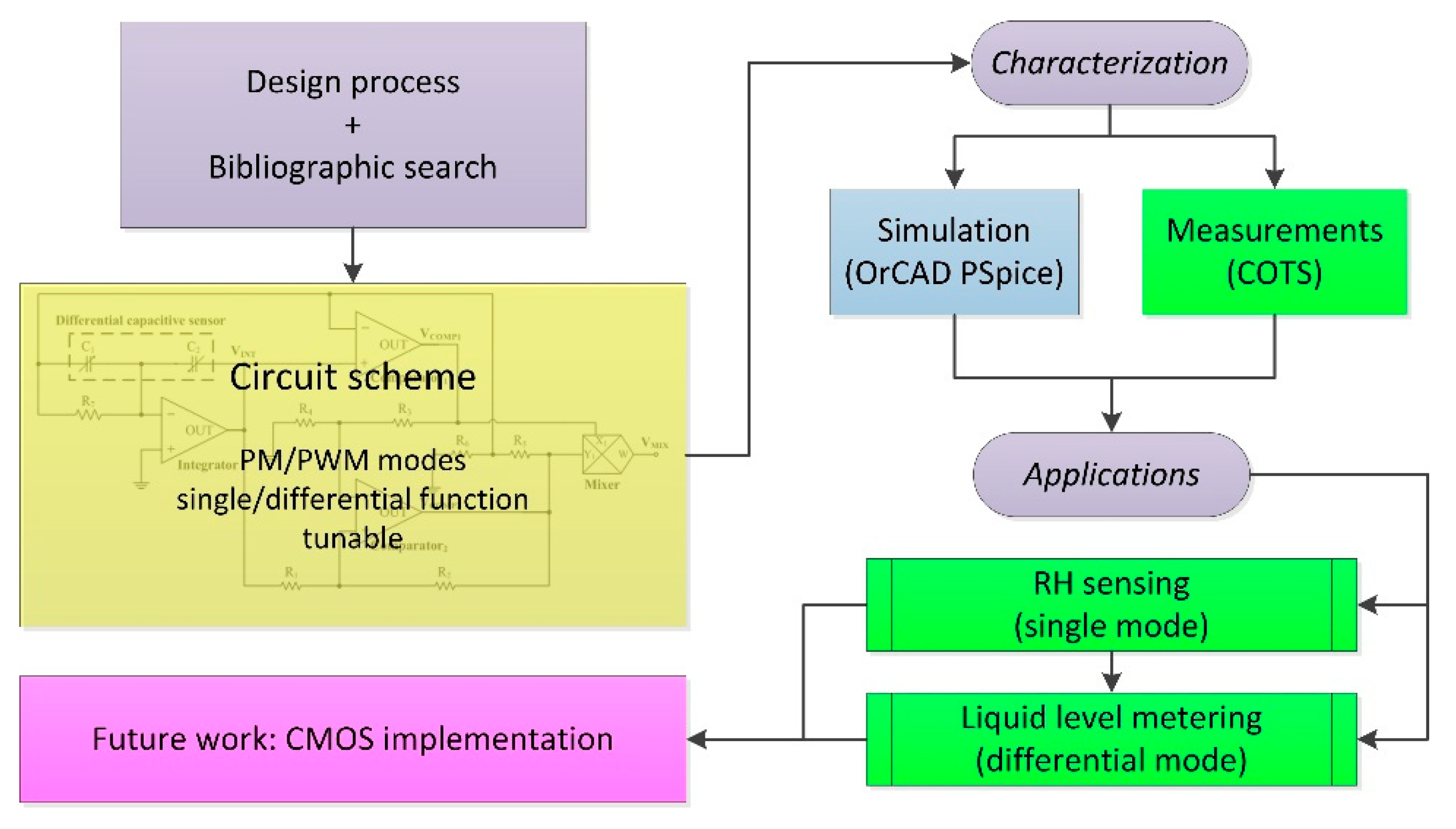
In this regard, here we propose a new low-cost portable solution of analogue electronic interface circuit performing a C-T conversion that is suitable for differential capacitive sensors with high detection sensitivity and resolution. The developed architecture is based on a relaxation oscillator whose generated square wave signal period and duty-cycle are linearly dependent from the differential capacitance variations combining both the PM and the PWM modulations. Through the setting of few resistor values, it is possible to regulate dynamic range, sensitivity, and resolution of the differential capacitance variation detection. Moreover, it shows a very low sensitivity to common-mode noise and disturbances, as well as to the effects due to the presence of parasitic elements at the circuit sensing nodes. The interface circuit has been designed and preliminary simulated in the OrCAD PSpice environment. Afterwards, after its implementation on a laboratory breadboard employing commercial discrete components, the proposed solution has been tested through experimental measurements confirming the theoretical calculations. In particular, sample components and commercial capacitive sensors have been employed, as well as an ad-hoc liquid level detection system has been fabricated and characterized validating the developed solution and its performances. The block diagram of the conducted research is depicted in Figure 1.
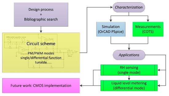
Figure 1.
Block diagram of the conducted research.
2. Materials and Methods
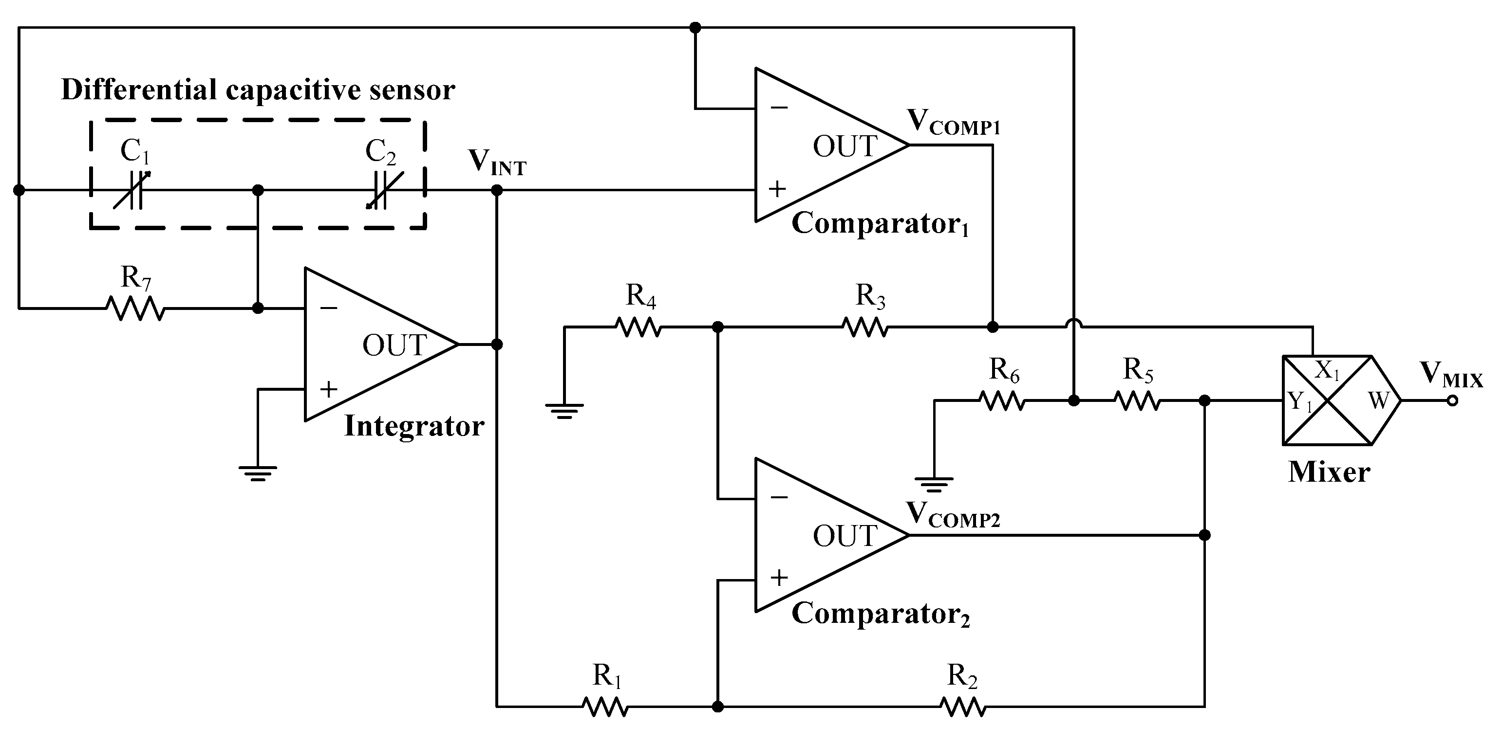
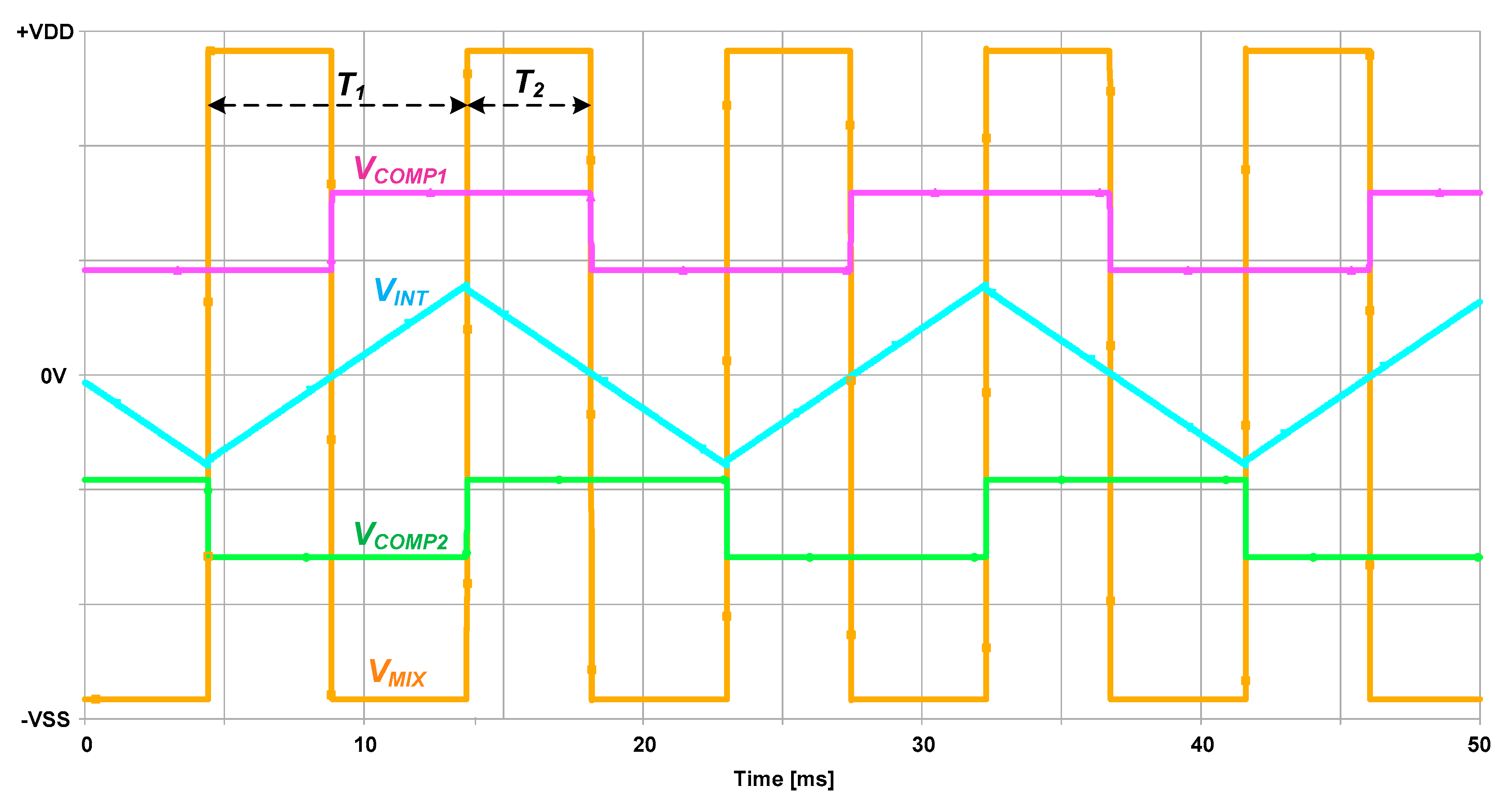
The proposed schematic circuit for differential capacitive sensors interfacing is reported in Figure 2, while Figure 3 shows an example of the time response of the circuit reporting the voltage signals at its main output nodes. This solution, designed with a reduced number of active (three Operational Amplifiers, OAs, and one Mixer) and passive (seven resistors) components, is based on a relaxation oscillator performing a C-T conversion through a closed multiple-feedback loop architecture combining both the PM and the PWM modulations. This avoids any calibration procedure and it reduces ground noise/disturbs (i.e., a very low sensitivity to common-mode noise/disturbs and to parasitic elements), while it allows for an auto-excitation of the differential capacitive sensor through the output AC square waveform. The designed architecture, in fact, intrinsically provides a square wave output (i.e., a “digitalized” output signal), which is independent from the supply voltage, so offering further benefits, such as immunity to voltage offsets and easiness in digital multiplexing and signal processing (e.g., its period and duty-cycle can be easily read by means of digital counters).
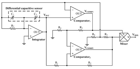
Figure 2.
Schematic circuit of the proposed electronic interface for differential capacitive sensors.
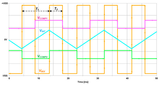
Figure 3.
Example of the time response of the proposed interface evaluating the voltage signals at its main nodes.
More in detail, the circuit is composed of a voltage integrator where the differential capacitive sensor is connected, two hysteresis voltage comparators that allow for regulating the dynamic range and the detection sensitivity and resolution through the use of seven resistors and a mixer that combine all the information providing an output pulsed signal whose period and duty-cycle depend on the two capacitances C1 and C2 of the differential capacitive sensor. In particular, the mixer also allows for reducing the measurement time, since the period of the output pulsed signal VMIX is equal to a semi-period (i.e., a double frequency) of the internal square wave signal VCOMP2 generated by the closed loop oscillator composed by the integrator and the two comparators. The mixer, in fact, receives at its input terminals the two square wave signals, VCOMP1 and VCOMP2, generating a further square waveform VMIX whose period T1 (that is half period of VCOMP1 and VCOMP2) and pulse width T2 (that is the overlapping time between VCOMP1 and VCOMP2, when they have both positive or negative values) have to be measured so as to estimate and calculate the capacitance values C1 and C2. Moreover, it is possible to easily set the interface working range (i.e., the sensor variation range) through the employed resistors, which also allow for fixing the desired detection sensitivity of the overall conditioning circuit.
Through a straightforward circuit node analysis, when considering ideal components, the time period T1 and the pulse width T2 of the generated output square waveform VMIX can be expressed, as follows:
from which (i.e., by inverting them) it is possible to achieve the following relationships to estimate/calculate the two components (i.e., C1 and C2) of the differential capacitive sensor as a function of the other circuit parameters and the time values T1 and T2:
It is worth noting that, since the circuit converts a differential capacitance into a pulsed signal, the initial values of C1 and C2 impose the starting oscillating period T1 and duty-cycle T2 of the output signal. Nevertheless, through the seven resistors it is possible to change these initial values, even if it acts also on the circuit detection range, sensitivity, and resolution. On the other hand, according to Equations (1) and (2), T1 and T2 are mostly/directly conditioned by resistor R7, which mainly regulates the charge/discharge of C1 and C2. Therefore, when dealing with small sensor capacitances (in the range of few pF), R7 is required to be high in order to set T1 and T2 in a range (e.g., in the order of μs or ms), which is more suitable for subsequent signal conditioning/processing stages as well as to optimize/maximize the circuit response/performance (i.e., the detectable capacitive variation range and the detection sensitivity/resolution of the interface circuit). For moderate detection of sensitivities/resolutions and/or high capacitive ranges (in the range of hundreds pF), the value of R7 can be reduced. Finally, if C1 = C2, the relationship between T1 and T2 can be simply expressed, as follows:
Moreover, we highlight that the output PWM signal can also be easily converted into a DC voltage signal through a low-pass filtering operation. In this way, the information on the duty-cycle of the output square waveform, also evaluated as the ratio T2/T1 taking into account the effects due to the variation of both the sensor capacitive elements C1 and C2 (i.e., the differential variation) is evaluated by extracting the DC level of the output pulsed signal VMIX (i.e., its mean value that is proportional to the differential capacitive sensor variation (C1 − C2)/(C1 + C2)) whose value can be ideally calculated, as follows:
being VSAT+ and VSAT− the output saturation levels of the mixer reached by VMIX signal. In this last case, the overall circuit can be consequently classified as a C-V converter.
3. Results
3.1. Simulations
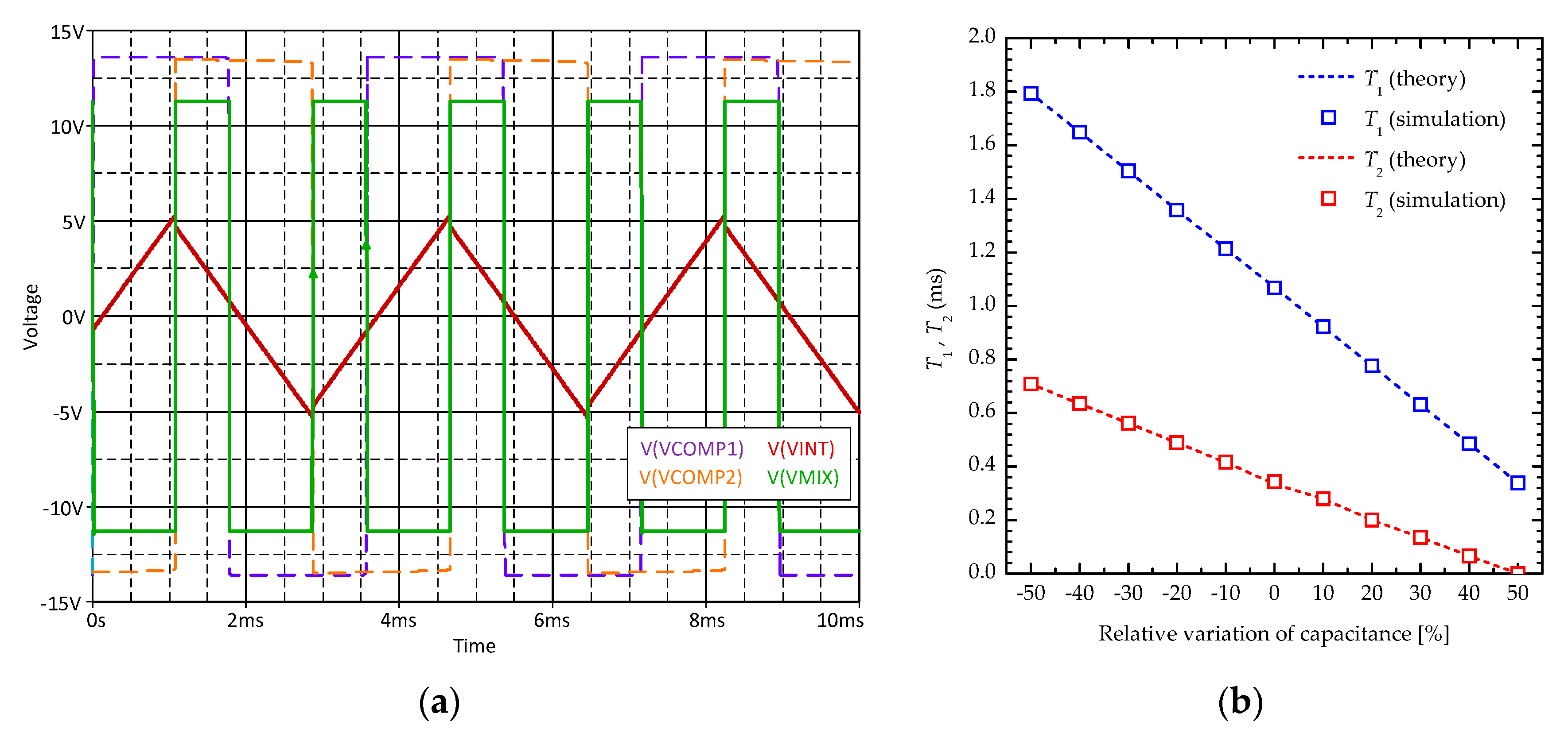
OrCAD PSpice simulations have been preliminary conducted employing low-noise JFET-input TL071 by Texas Instruments as OAs and AD633 by Analog Devices as analog multiplier (i.e., mixer) all being supplied at ±15 V. Different values of the baseline of the differential capacitive sensor have been considered (i.e., C1 = C2 = C0 = 2.2 pF, 10 pF, 100 pF, and 180 pF), so to demonstrate the circuit suitability with different kind of commercial and ad-hoc integrated sensors (with responses linear, hyperbolic, etc.). In Figure 4, the simulation results are reported and compared with the related theoretical values (from Equations (1) and (2)) of the period T1 and the pulse width T2 of output square waveform VMIX as a function of the relative variation the differential capacitive sensor (i.e., 100 × (C1 − C2)/(C1 + C2)) showing high linearity (i.e., R2 = 0.9997) and high sensitivity S (i.e., ST1 = 0.145 ms/pF; ST2 = 0.071 ms/pF). In particular, Figure 4a shows an example of the time response of the circuit when considering the voltage signals at its main nodes for C1 = 5 pF and C2 = 15 pF (i.e., considering C0 = 10 pF and a differential capacitance variation equal to −50%). In addition, Figure 4b reports the T1 and T2 time values that were achieved when considering a sensor baseline C1 = C2 = C0 = 10 pF (i.e., the central/initial value) and its relative variation of ±50%, so that the differential capacitance (i.e., C1 − C2) is changed from −10 pF to +10 pF. In particular, C1 changes from 5 pF to 15 pF, while C2 varies from 15 pF to 5 pF with a differential capacitance variation step equal to 2 pF (i.e., each single capacitive element varies in opposite way with a step of 1 pF). Moreover, the reported results have been achieved by setting the circuit resistors, as follows: R1 = 1 kΩ, R2 = 3 kΩ, R3 = 20 kΩ, R4 = 1 kΩ, R5 = 15 kΩ, R6 = 1 kΩ and R7 = 10 MΩ.

Figure 4.
(a) Example of the time response of the circuit; and, (b) simulation results together with the corresponding theoretical data of the period T1 and the pulse width T2 of output square waveform VMIX as a function of the relative variation the differential capacitive sensor for C1 = C2 = C0 = 10 pF.
Moreover, further simulations have been conducted in order to evaluate the effects on the circuit of operating temperature variations. More in detail, we have considered/referred to commercial and industrial applications, so simulating the circuit from −20 °C up to 85 °C. In particular, referring to the circuit set-up considered for the capacitive variation range of 5–15 pF for C1 and C2, the resulting maximum relative variations of T1 and T2 at −20 °C is lower than 0.6%, while at +85 °C it is lower than 9%. These values correspond to maximum relative errors that are lower than 10% at −20 °C and lower than 7% at +85 °C in the estimation of C1 and C2 values.
3.2. Preliminary Experimental Measurements
Basic experimental measurements have been performed implementing the circuit on a laboratory breadboard employing commercial discrete components as well as capacitive sensors. In this case, the differential capacitance (i.e., C1 − C2) is varied from −15.8 pF to +15.8 pF using commercial high-precision high-accuracy discrete capacitors, calibrated/measured by using an ISO-TECH LCR821 high-precision high-accuracy LCR-meter (accuracy better than 0.5%) verifying the maximum deviation from the capacitance nominal value lower than 1%. In particular, C1 has been changed from 2.2 pF to 18 pF (i.e., 2.2 pF, 4.7 pF, 8.2 pF, 10 pF, 12 pF, 15 pF, 18 pF) and C2 from 18 pF to 2.2 pF (i.e., 18 pF, 15 pF, 12 pF, 10 pF, 8.2 pF, 4.7 pF, 2.2 pF), while keeping constant the total capacitance value C1 + C2 at about 20 pF (C0 = 10 pF). In order to get oscillating periods of few milliseconds and to achieve better results, the following resistance values have been chosen: R1 = 1 kΩ, R2 = 1.2 kΩ, R3 = 15 kΩ, R4 = 1 kΩ, R5 = 47 kΩ, R6 = 1 kΩ, R7 = 10 MΩ. The parasitic capacitance of the resistors was measured, giving values below 0.5 pF. The resulting measurements of the period T1 and the pulse width T2 have been performed while employing a GPIB-based experimental setup and a National Instruments LABVIEW-based automatic acquisition system, including conventional instrumentations, such as a frequency-meter Agilent 34970A (accuracy better than 0.01%), a Data Acquisition/Switch Unit, and digital multimeter Agilent 34401A (accuracy better than 0.01%), as well as an oscilloscope Tektronix TPS2024R.
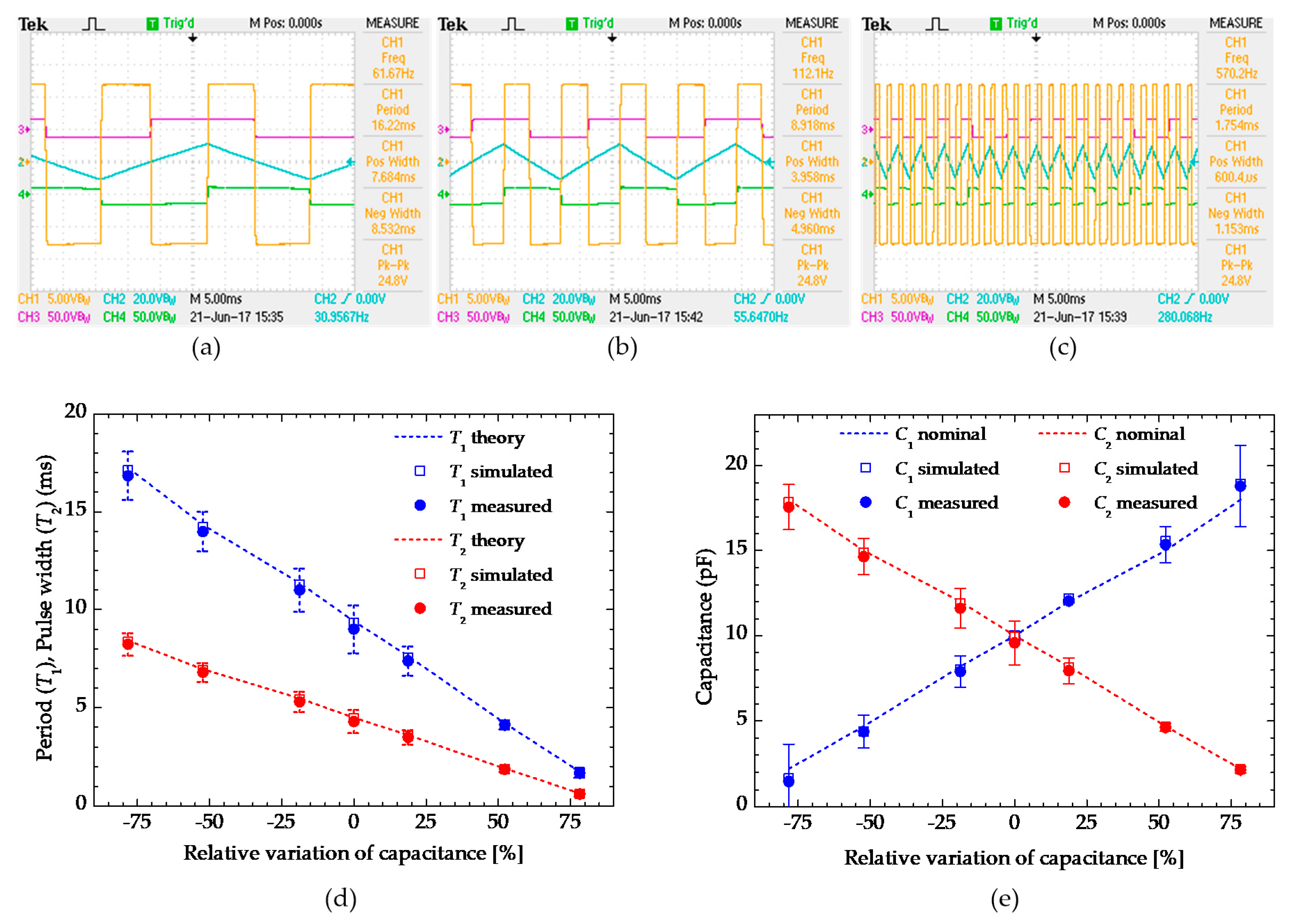
More in detail, firstly we proved the period and pulse width modulations as a function of the variation of the differential capacitance confirming their proportional linearly dependence. The oscillograms are reported in Figure 5a–c that demonstrate the proper functionality of the proposed interface circuit showing its main signals (in particular, the generated output square waveform VMIX) and the corresponding measured values of T1 (i.e., CH1 Period in the right part of each picture) and T2 (i.e., CH1 Pos Width in the right part of each picture) for three different sets of C1 and C2 values: Figure 5a, C1 = 2.2 pF and C2 = 18 pF; Figure 5b, C1 = C2 = 10 pF; Figure 5c, C1 = 18 pF and C2 = 2.2 pF. The overall measurement results are reported in Figure 5d showing the oscillation period T1 and the pulse width T2 as function of the differential capacitance variation (i.e., 100 × (C1 − C2)/(C1 + C2)), which are in a good agreement with the theoretical calculations according Equations (1) and (2) and with the related simulation results achieved with the same operating conditions. In this case, the achieved sensitivities with respect to T1 and T2 are ST1 = 0.982 ms/pF and ST2 = 0.491 ms/pF, respectively (linearity correlation coefficient R2 of about 0.999). On the other hand, taking into account the measured values of T1 and T2, Figure 5e reports on the estimated values of C1 and C2 capacitances calculated through the Equations (3) and (4). The corresponding relative error, evaluated between the measured/estimated capacitance values and its nominal/real values, is lower than 3%. Finally, the maximum averaged RMS jitter level, measured on the rising/falling edges of the output square wave signal VMIX, results to be always lower than 50 ns, so that the resulting estimated minimum detectable differential capacitance variation (i.e., the best theoretical detection resolution of the circuit) is about 0.1 fF. The average power consumption of the overall electronic interface circuit is about 68 mW.
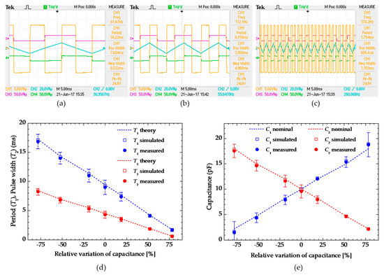
Figure 5.
Measured main output signals of the circuit for (a) C1 = 2.2 pF and C2 = 18 pF, (b) C1 = C2 = 10 pF, and (c) C1 = 18 pF and C2 = 2.2 pF; (d) measured, simulated and theoretical oscillation periods T1 and pulse widths T2 as a function of the relative differential capacitance variation; (e) calculated/estimated capacitance values.
3.3. Relative Humidity (RH) Sensor
In order to evaluate the potentiality of the proposed circuit as electronic interface in real capacitive sensing applications, we arranged an experimental set-up for the measurement of the Relative Humidity (RH) making use of the commercial capacitive sensor HS1101LF by Sensor Solutions—Measurement Specialties and a climatic chamber Challenge CH600 by ACS—Angelantoni Industries. The employed capacitive sensor provides a nominal capacitance value of about 180 pF @ 55% RH and it can be biased/excited in the operating range [5 kHz–300 kHz] with AC voltage signals up to 10 V.
In this regard, for preliminary setting/testing and optimization of the circuit, we made use of commercial high-precision high-accuracy discrete capacitors, calibrated/measured by using the ISO-TECH LCR821 LCR-meter showing a maximum deviation of lower than 1%. In particular, the capacitor C1 has been fixed to a value equal to 180 pF (i.e., C0 = 180 pF), while performing a sweep of the C2 capacitance in the variation range [160 pF–197 pF] by means of a fixed 150 pF capacitor in parallel with others having smaller different values (i.e., C2 = 150 pF + [10 pF; 12 pF; 15 pF; 18 pF; 22 pF; 27 pF; 30 pF; 33 pF; 39 pF; 47 pF]). In this case, the following resistance values have been set so to optimize the interface circuit response: R1 = 470 Ω, R2 = 560 Ω, R3 = 2.2 kΩ, R4 = 470 Ω, R5 = 4.7 kΩ, R6 = 470 Ω, R7 = 47 kΩ. The employed experimental set-up and measurement instrumentations are those ones already previously reported and described in Section 3.1.
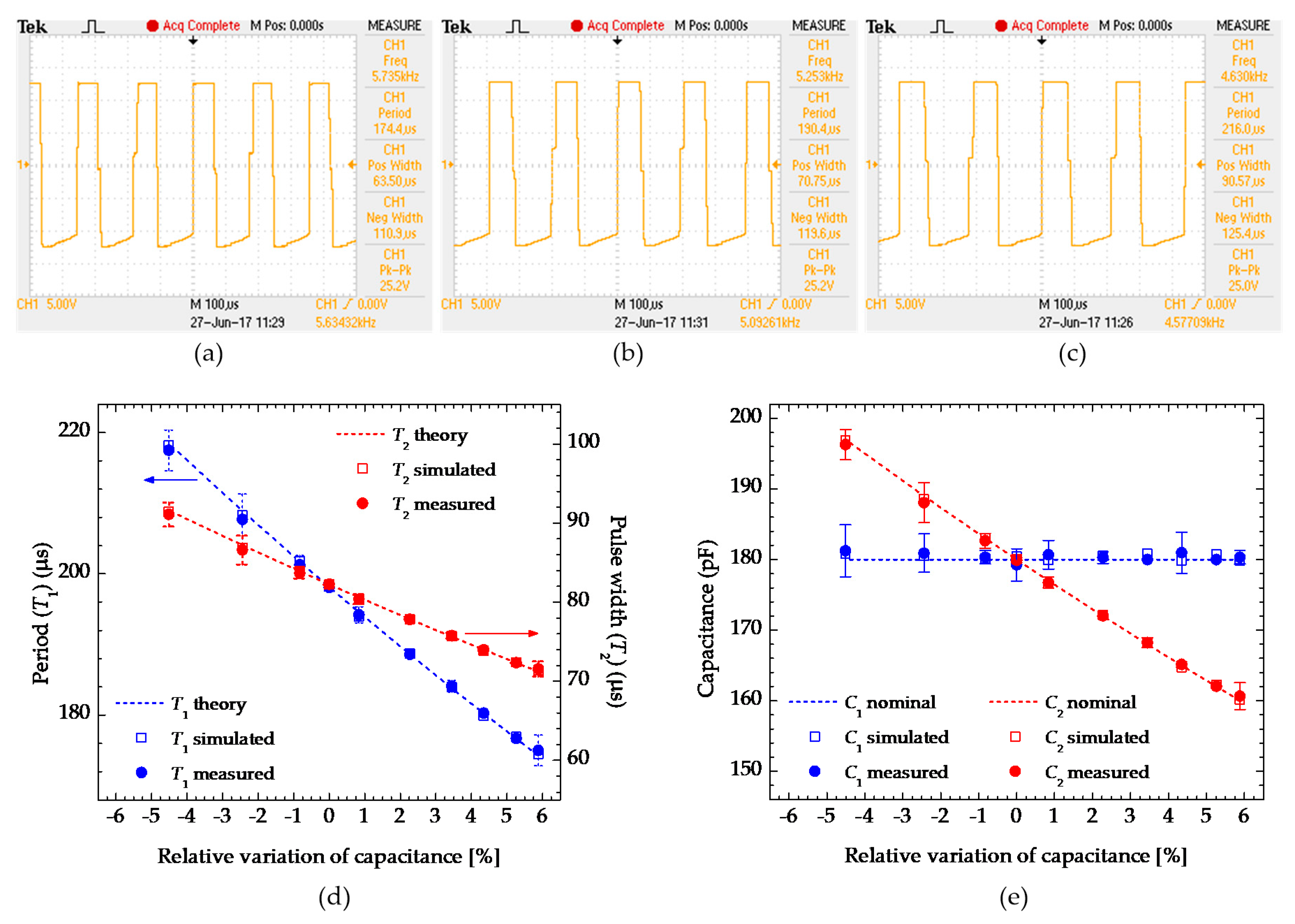
The overall obtained results are shown in Figure 6. In particular, Figure 6a–c report the oscillograms showing the circuit main output square waveform VMIX, including the corresponding measured values of the period T1 (i.e., CH1 Period in the right part of each picture) and the pulse width T2 (i.e., CH1 Pos Width in the right part of each picture). They demonstrate the proper performances of the circuit for an operating configuration with a fixed value of C1 = 180 pF and three different values of C2: Figure 6a, C2 = 160 pF; Figure 6b, C2 = 180 pF; Figure 6c, C2 = 197 pF.
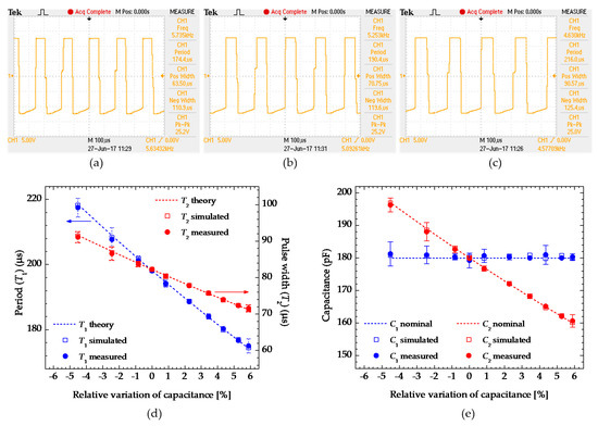
Figure 6.
Oscillograms showing the output voltage signal VMIX that demonstrates the proper performances of the circuit for a configuration employing a fixed C1 = 180 pF and (a) C2 = 160 pF, (b) C2 = 180 pF, and (c) C2 = 197 pF; (d) measured, simulated, and theoretical oscillation periods T1 and pulse widths T2 as a function of the relative differential capacitance variation; (e) calculated/estimated capacitance values.
Furthermore, Figure 6d shows the overall measurement results reporting the oscillation period T1 and the pulse width T2 as function of the relative capacitance variation (i.e., 100 × (C1 − C2)/(C1 + C2)) achieved by changing C2 in the range [160 pF–197 pF]. The collected data confirm the correct functionalities of the interface circuit agreeing with the theoretical calculations, from Equations (1) and (2), and also with the corresponding simulations performed when considering the same circuit parameters. From these results, the two detection sensitivities ST1 = 0.001 ms/pF and ST2 = 0.0006 ms/pF with respect to T1 and T2, respectively, have been calculated (linearity correlation coefficient R2 of about 0.999) so as to evaluate/estimate the performances of the circuit, especially in terms of the minimum detection resolution of differential capacitance variations that, in this case, is about 83 fF (considering a maximum averaged RMS jitter level, measured on the rising/falling edges of VMIX, lower than 50 ns). Finally, starting from these results and by employing Equations (3) and (4), the values of C1 and C2 capacitances have been estimated/calculated, as reported in Figure 6d showing a relative error, evaluated between the measured/estimated capacitance values and its nominal/real values, lower than 0.5 %.
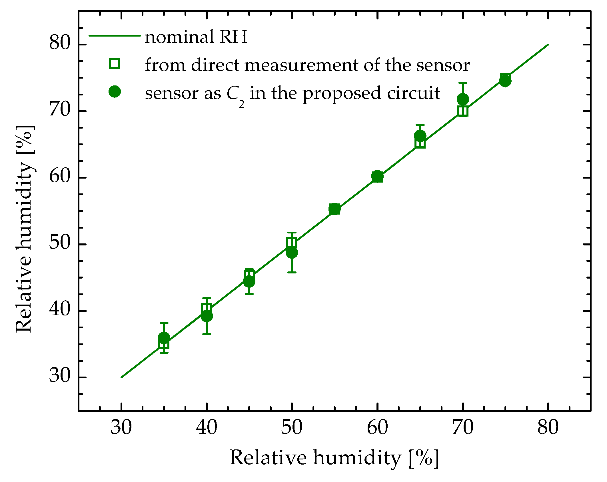
Successively, the C2 capacitor has been replaced by the commercial HS1101LF RH capacitive sensor, so performing through the controlled climatic chamber a sweep in the RH from 35% to 75%, with steps of 5% and room temperature set to 25 °C. The achieved results are reported in Figure 7 comparing the calculated/estimated RH% with the fixed nominal values as well as with the values that were achieved from direct measurement of the sensor by using the ISO-TECH LCR821 high-precision high-accuracy LCR-meter and extracting the data from sensor datasheet. The reported data have been extracted starting from the measurement of the time period T1 and the pulse width T2 as a function of the RH% variation with detection sensitivities of about ST1 = 0.0004 ms/RH% and ST2 = 0.0002 ms/RH% with respect to T1 and T2, respectively. Subsequently, the values of the capacitances C1 and C2 have been estimated/calculated by employing Equations (3) and (4). Finally, from the information reported in the datasheet of the used commercial capacitive sensor, the RH% values have been extracted employing the reverse polynomial response equation reported in the same device datasheet. In this case, the relative error, evaluated between the measured/estimated values and nominal/real values, is lower than 3% and the minimum estimated detection resolution in terms of the RH% variation is about 0.25% (considering a maximum averaged RMS jitter level, measured on the rising/falling edges of VMIX, lower than 50 ns).
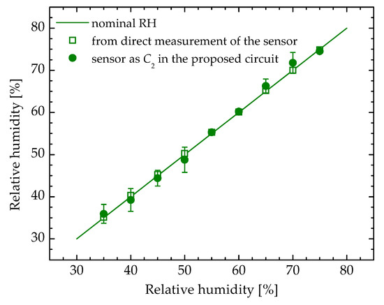
Figure 7.
Experimental results concerning the measurement of RH% performed by employing a commercial capacitive sensor.
3.4. Liquid Level
Lastly, we developed a liquid level meter, with the aim of evaluating the performance of the proposed electronic interface in real differential capacitance measurement applications. The considered experimental apparatus is depicted in Figure 8. A plexiglas-based cube with a volume lower than 1 ℓ is provided with three Cu-based conductive plates. Two of them are fixed at the top and bottom faces, while the other floats onto the top liquid surface keeping the horizontality through the use of a polystyrene plate fixed under the Cu plate (i.e., the combined plates work like a float). In this way, two complementary (differential) capacitors having a common element (i.e., common plate) are formed: one with liquid (i.e., distilled water) as the dielectric forming the capacitor C1 and the other with the air providing the capacitor C2.
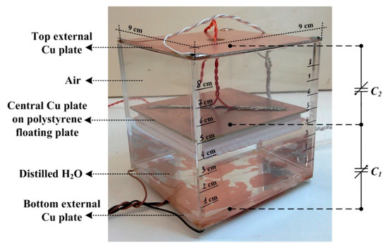
Figure 8.
Developed liquid level meter employed as differential capacitive sensor.
This apparatus has been employed as differential capacitive sensor measured through the developed interface circuit. More in detail, the distilled water level has been changed from 1 cm to 7 cm, with steps of 1 cm, so moving the common central floating plate that provides a simultaneous variation of C1 and C2 capacitance values. Moreover, in order to optimize the interface circuit response, the following resistance values have been considered: R1 = 1 kΩ, R2 = 1.2 kΩ, R3 = 15 kΩ, R4 = 1 kΩ, R5 = 47 kΩ, R6 = 1 kΩ, R7 = 10 MΩ. The overall experimental measurement results are reported in Figure 8, when considering that the two capacitors C1 and C2 have been connected to the circuit both, as depicted in Figure 8 (see results of Figure 9a) and by interchanging their positions/connections (i.e., C1 used as C2, and vice versa; see results of Figure 9b). In particular, by measuring the time period T1 and the pulse width T2 values of the circuit main output signal VMIX as a function of the liquid level, the C1 and C2 capacitance values have been calculated/estimated through the Equations (3) and (4) and compared with the capacitive values of the same elements achieved from direct measurements through the ISO-TECH LCR821 high-precision high-accuracy LCR-meter. In this last case, the resulting relative error, as calculated among the obtained experimental data, is always lower than 5%, both for the capacitor with higher values and for the capacitor with lower values. The minimum estimated detection resolution in terms of the liquid level variation is about 0.01 mm (considering a maximum averaged RMS jitter level, measured on the rising/falling edges of VMIX, lower than 50 ns). Additional simulation analyses have been also performed, so demonstrating a low sensitivity to common-mode noise and disturbances as well as, in particular, an excellent immunity to additional parasitic capacitances at the main circuit sensing nodes. More in detail, at each terminal node of the differential capacitive sensor connected to the circuit (i.e., the three main input nodes of the interface), a 10 pF grounded capacitor has been considered and added as an external parasitic component (i.e., as a parasitic capacitance provided by a differential capacitive sensor, as those ones related to the plates of C1 and C2 of the box shown in Figure 8). In this sense, referring to the circuit set-up considered for the simulation results reported in Section 3.1, and thus considering the capacitive variation range of 5–15 pF for C1 and C2, the resulting maximum relative variation of T1 and T2 is lower than 0.25% that, on the other hand, corresponds to a maximum relative error lower than 8% in the estimation of C1 and C2 values.
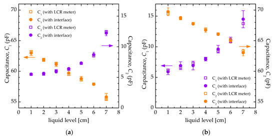
Figure 9.
(a) Experimental results achieved by using the developed liquid level meter as differential capacitive sensor reported in Figure 8, (b) after interchanging C1 and C2.
4. Discussion
As a final remark, Table 1 summarizes the main performances and the experimental characteristics of the proposed circuit compared with other similar solutions presented in the literature having linear responses and based on C-T conversion architectures. As it can be seen, the presented circuit is an analogue solution that manages differential capacitive sensors combining PM and PWM techniques and, even if only implemented on breadboard with discrete commercial components, shows very satisfactory characteristics, especially in terms of high detection sensitivity, good detection range, and minimum detection resolution.

Table 1.
Main performance parameters of the proposed circuit as compared to other similar solutions based on C-T conversion.
5. Conclusions
A simple interface circuit, operating a capacitance-to-time conversion by means of an oscillator-based topology, suitable for the readout of differential capacitive sensors has been presented. The multiple-feedback circuit architecture, employing only four active components (three OAs and one mixer) and seven resistors, provides an AC sensor excitation voltage, reduces ground noise disturbs, and avoids system calibrations. By performing a PM and a PWM modulations, the provided output square wave signal results in being linearly proportional to the sensor differential capacitance values. The sensor variation range and the detection sensitivity can be easily set through the employed resistors. PSpice simulations, together with all the experimental measurements, performed by implementing the circuit on a laboratory breadboard and using commercial discrete components, have validated the proposed idea showing a good agreement with theoretical calculations within an overall capacitive variation range that is equal to [2.2 pF–197 pF] and achieving a minimum capacitance detection resolutions as low as 0.1 fF for a differential capacitive variation range equal to ±15.8 pF. Moreover, the simple schematic of the proposed circuit makes it suitable to be designed at the transistor level in a Si-based standard CMOS integrated technology for integrated portable sensor applications, also employing different kinds of differential capacitive sensing devices, such as MEMS, force/position, and humidity sensors.
Author Contributions
Conceptualization, A.D.M.; methodology, A.D.M., M.-D.C.-B. and C.R.; formal analysis, A.D.M., M.-D.C.-B. and C.R.; investigation, A.D.M.; resources, C. Reig.; writing—original draft preparation, A.D.M.—review and editing, A.D.M., M.-D.C.-B. and C.R.; visualization, C.R.; project administration, A.D.M. and C.R.; funding acquisition, A.D.M. and C.R.
Funding
This research was partially funded by University of Valencia, with the grant program “Attracting Talent”—VLC CAMPUS 2015.
Acknowledgments
The co-author Andrea De Marcellis acknowledges the Research Fellowship from the University of Valencia (Sub-Program “Attracting Talent”—VLC CAMPUS 2015).
Conflicts of Interest
The authors declare no conflict of interest.
References
- Yuan, J.S.; Bi, Y. Process and temperature robust voltage multiplier design for RF energy harvesting. Micorelectron. Reliab. 2015, 55, 107–113. [Google Scholar] [CrossRef]
- Bi, Y.; Gaillardon, P.E.; Hu, X.S.; Niemier, M.; Yuan, J.S.; Jin, Y. Leveraging Emerging Technology for Hardware Security—Case Study on Silicon Nanowire FETs and Graphene SymFETs. In Proceedings of the 2014 IEEE 23rd Asian Test Symposium, Hangzhou, China, 16–19 November 2014; pp. 342–347. [Google Scholar] [CrossRef]
- Bi, Y.; Shamsi, K.; Yuan, J.S.; Jin, Y.; Niemier, M.; Hu, X.S. Tunnel FET Current Mode Logic for DPA-Resilient Circuit Designs. IEEE Trans. Emerg. Top. Comput. 2017, 5, 340–352. [Google Scholar] [CrossRef]
- Chen, X.; Brox, D.; Assadsangabi, B.; Ali, M.S.M.; Takahata, K. A stainless-steel-based implantable pressure sensor chip and its integration by microwelding. Sens. Actuators A Phys. 2017, 257, 134–144. [Google Scholar] [CrossRef]
- Apigo, D.J.; Bartholomew, P.L.; Russell, T.; Kanwal, A.; Farrow, R.C.; Thomas, G.A. An Angstrom-sensitive, differential MEMS capacitor for monitoring the milliliter dynamics of fluids. Sens. Actuators A Phys. 2016, 251, 234–240. [Google Scholar] [CrossRef] [PubMed]
- Rivadeneyra, A.; Fernández-Salmerón, J.; Agudo-Acemel, M.; López-Villanueva, J.A.; Capitan-Vallvey, L.F.; Palma, A.J. Printed electrodes structures as capacitive humidity sensors: A comparison. Sens. Actuators A Phys. 2016, 244, 56–65. [Google Scholar] [CrossRef]
- Aydemir, A.; Terzioglu, Y.; Akin, T. A new design and a fabrication approach to realize a high performance three axes capacitive MEMS accelerometer. Sens. Actuators A Phys. 2016, 244, 324–333. [Google Scholar] [CrossRef]
- Rahman, M.D.T.; Rahimi, A.; Gupta, S.; Panat, R. Microscale additive manufacturing and modeling of interdigitated capacitive touch sensors. Sens. Actuators A Phys. 2016, 246, 94–103. [Google Scholar] [CrossRef]
- Liu, Y.T.; Kuo, Y.L.; Yan, D.W. System integration for on-machine measurement using a capacitive LVDT-like contact sensor. Adv. Manuf. 2017, 5, 50–58. [Google Scholar] [CrossRef]
- Bai, Y.; Lu, Y.; Hu, P.; Wang, G.; Xu, J.; Zeng, T.; Li, Z.; Zhang, Z.; Tan, J. Absolute position sensing based on a robust differential capacitive sensor with a grounded shield window. Sensors 2016, 16, 680. [Google Scholar] [CrossRef]
- Park, S.H.; Kim, H.S.; Bang, J.S.; Cho, G.H.; Cho, G.H. A 0.26-nJ/node, 400-kHz Tx driving, filtered fully differential readout IC with parasitic RC time delay reduction technique for 65-in 169 × 97 capacitive-type touch screen panel. IEEE J. Solid-State Circuits 2017, 52, 528–542. [Google Scholar] [CrossRef]
- Liu, X.; Peng, K.; Chen, Z.; Pu, H.; Yu, Z. A new capacitive displacement sensor with nanometer accuracy and long range. IEEE Sens. J. 2016, 16, 2306–2316. [Google Scholar] [CrossRef]
- Ciccarella, P.; Carminati, M.; Sampietro, M.; Ferrari, M. Multichannel 65zF RMS resolution CMOS monolithic capacitive sensor for counting single micrometer-sized airborne particles on chip. IEEE J. Solid-State Circuits 2016, 51, 2545–2553. [Google Scholar] [CrossRef]
- Wu, X.; Deng, F.; Hao, Y.; Fu, Z.; Zhang, L. Design of a humidity sensor tag for passive wireless applications. Sensors 2015, 15, 25564–25576. [Google Scholar] [CrossRef] [PubMed]
- Arefin, M.S.; Redouté, J.M.; Yuce, M.R. A MEMS interface IC with low-power and wide-range frequency-to-voltage converter for biomedical applications. IEEE Trans. Biomed. Circuits Syst. 2016, 10, 455–466. [Google Scholar] [CrossRef] [PubMed]
- Constandinou, T.G.; Georgiou, J.; Toumazou, C. A micropower front-end interface for differential-capacitive sensor systems. In Proceedings of the 2008 IEEE International Symposium on Circuits and Systems, Seattle, WA, USA, 18–21 May 2008; pp. 2474–2477. [Google Scholar] [CrossRef]
- Mochizuki, K.; Watanabe, K.; Masuda, K. A high-accuracy high-speed signal processing circuit of differential-capacitance transducers. IEEE Trans. Instrum. Meas. 1998, 47, 1244–1247. [Google Scholar] [CrossRef]
- Singh, T.; Saether, T.; Ytterdal, T. Current-mode capacitive sensor interface circuit with single-ended to differential output capability. IEEE Trans. Instrum. Meas. 2009, 58, 3914–3920. [Google Scholar] [CrossRef]
- Royo, G.; Sánchez-Azqueta, C.; Gimeno, C.; Aldea, C.; Celma, S. Programmable low-power low-noise capacitance to voltage converter for MEMS accelerometers. Sensors 2017, 17, 67. [Google Scholar] [CrossRef] [PubMed]
- Scotti, G.; Pennisi, S.; Monsurro, P.; Trifiletti, A. 88-μA 1-MHz stray-insensitive CMOS current-mode interface IC for differential capacitive sensors. IEEE Trans. Circuits Syst. 2014, 61, 1905–1916. [Google Scholar] [CrossRef]
- Kyriakis-Bitzaros, E.D.; Stathopoulos, N.A.; Pavlos, S.; Goustouridis, D.; Chatzandroulis, S. A reconfigurable multichannel capacitive sensor array interface. IEEE Trans. Instrum. Meas. 2011, 60, 3214–3221. [Google Scholar] [CrossRef]
- Wang, S.; Koickal, T.J.; Hamilton, A.; Mastropaolo, E.; Cheung, R.; Abel, A.; Smith, L.S.; Wang, L. A power-efficient capacitive read-out circuit with parasitic-cancellation for MEMS cochlea sensors. IEEE Trans. Biomed. Circuits Syst. 2016, 10, 25–37. [Google Scholar] [CrossRef]
- Ignjatovic, Z.; Bocko, M.F. An interface circuit for measuring capacitance changes based upon capacitance-to-duty cycle (CDC) converter. IEEE Sens. J. 2005, 5, 403–410. [Google Scholar] [CrossRef]
- De Marcellis, A.; Ferri, G.; Mantenuto, P. A CCII-based non-inverting Schmitt trigger and its application as astable multivibrator for capacitive sensor interfacing. Int. J. Circuit Theory Appl. 2016, 45, 1060–1076. [Google Scholar] [CrossRef]
- Bruschi, P.; Nizza, N.; Piotto, M. A current-mode, dual slope, integrated capacitance-to-pulse duration converter. IEEE J. Solid-State Circuits 2007, 42, 1884–1891. [Google Scholar] [CrossRef]
- Tan, Z.; Shalmany, S.H.; Meijer, G.C.M.; Pertijs, M.A.P. An energy-efficient 15-bit capacitive-sensor interface based on period modulation. IEEE J. Solid-State Circuits 2012, 47, 1703–1711. [Google Scholar] [CrossRef]
- He, Y.; Chang, Z.Y.; Pakula, L.; Shalmany, S.H.; Pertijs, M.A.P. A 0.05 mm2 1 V capacitance-to-digital converter based on period modulation. In Proceedings of the IEEE International Solid-State Circuits Conference (ISSCC), San Francisco, CA, USA, 22–26 February 2015; pp. 1–3. [Google Scholar] [CrossRef]
- Nizza, N.; Dei, M.; Butti, F.; Bruschi, P. A low-power interface for capacitive sensors with PWM output and intrinsic low pass characteristic. IEEE Trans. Circuits Syst. 2013, 60, 1419–1431. [Google Scholar] [CrossRef]
- Lu, J.H.L.; Inerowicz, M.; Joo, S.; Kwon, J.K.; Jung, B. A low-power wide-dynamic-range semi-digital universal sensor readout circuit using pulsewidth modulation. IEEE Sens. J. 2011, 11, 1134–1144. [Google Scholar] [CrossRef]
- Sheu, M.L.; Hsu, W.H.; Tsao, L.J. A capacitance-ratio-modulated current front-end circuit with pulsewidth modulation output for a capacitive sensor interface. IEEE Trans. Instrum. Meas. 2012, 61, 447–455. [Google Scholar] [CrossRef]
- Arefin, M.S.; Redouté, J.M.; Yuce, M.R. A low-power and wide-range MEMS capacitive sensors interface IC using pulse-width modulation for biomedical applications. IEEE Sens. J. 2016, 16, 6745–6754. [Google Scholar] [CrossRef]
- Brookhuis, R.A.; Lammerink, T.S.J.; Wiegerink, R.J. Differential capacitive sensing circuit for a multi-electrode capacitive force sensor. Sens. Actuators A Phys. 2015, 234, 168–179. [Google Scholar] [CrossRef]
- Aezinia, F.; Bahreyni, B. Low-power parasitic-insensitive interface circuit for capacitive microsensors. IET Circuits Device Syst. 2016, 10, 104–110. [Google Scholar] [CrossRef]
- De Marcellis, A.; Cubells-Beltrán, M.D.; Reig, C.; Madrenas, J.; Zadov, B.; Paperno, E.; Cardoso, S.; Freitas, P.P. Quasi-digital front-ends for current measurement in integrated circuits with GMR technology. IET Circuits Device Syst. 2014, 8, 291–300. [Google Scholar] [CrossRef]
- Mohan, N.M.; Shet, A.R.; Kedarnath, S.; Kumar, V.J. Digital converter for differential capacitive sensors. IEEE Trans. Instrum. Meas. 2008, 57, 2576–2581. [Google Scholar] [CrossRef]
- Reverter, F.; Casas, O. Interfacing differential capacitive sensors to microcontrollers: A direct approach. IEEE Trans. Instrum. Meas. 2010, 59, 2763–2769. [Google Scholar] [CrossRef]
- Nabovati, G.; Ghafar-Zadeh, E.; Mirzaei, M.; Ayala-Charca, G.; Awwad, F.; Sawan, M. A new fully differential CMOS capacitance to digital converter for lab-on-chip applications. IEEE Trans. Biomed. Circuits Syst. 2015, 9, 353–361. [Google Scholar] [CrossRef] [PubMed]
- Omran, H.; Arsalan, M.; Salama, K.N. An integrated energy-efficient capacitive sensor digital interface circuit. Sens. Actuators A Phys. 2014, 216, 43–51. [Google Scholar] [CrossRef]
- Shin, D.Y.; Lee, H.; Kim, S. A delta–sigma interface circuit for capacitive sensors with an automatically calibrated zero point. IEEE Trans. Circuits Syst. II Express Briefs 2011, 58, 90–94. [Google Scholar] [CrossRef]
- Alhoshany, A.; Omran, H.; Salama, K.N. A 45.8 fJ/step, energy-efficient, differential SAR capacitance-to-digital converter for capacitive pressure sensing. Sens. Actuators A Phys. 2016, 245, 10–18. [Google Scholar] [CrossRef]
- Tan, Z.; Daamen, R.; Humbert, A.; Ponomarev, Y.V.; Chae, Y.; Pertijs, M.A.P. A 1.2-V 8.3-nJ CMOS humidity sensor for RFID applications. IEEE J. Solid-State Circuits 2013, 48, 2469–2477. [Google Scholar] [CrossRef]
- Oh, S.; Lee, Y.; Wang, J.; Foo, Z.; Kim, Y.; Blaauw, D. Dual-slope capacitance to digital converter integrated in an implantable pressure sensing system. In Proceedings of the 40th European Solid State Circuits Conference (ESSCIRC), Venice, Italy, 22–26 September 2014; pp. 295–298. [Google Scholar] [CrossRef]
© 2019 by the authors. Licensee MDPI, Basel, Switzerland. This article is an open access article distributed under the terms and conditions of the Creative Commons Attribution (CC BY) license (http://creativecommons.org/licenses/by/4.0/).

