The Reentrant Four-Layer Quasi-Elliptic Bandstop Filter

 ,
, 
Abstract
:1. Introduction
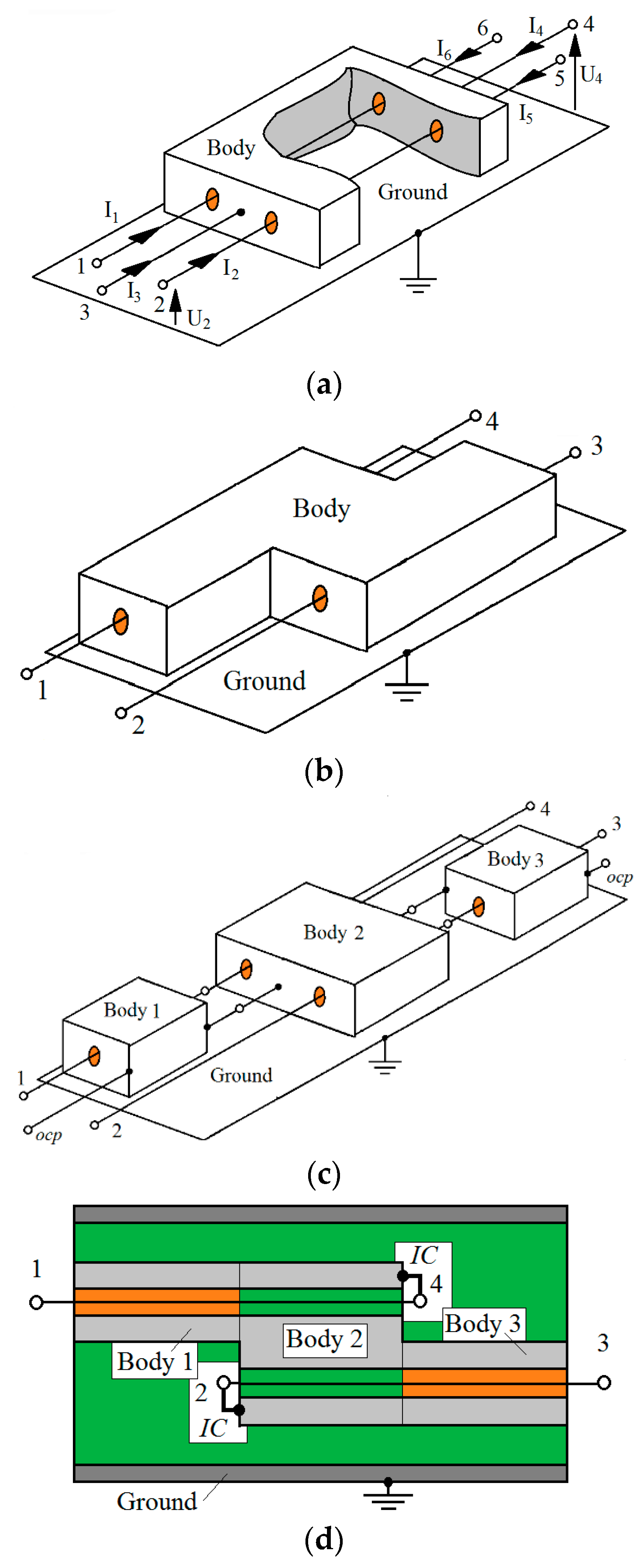
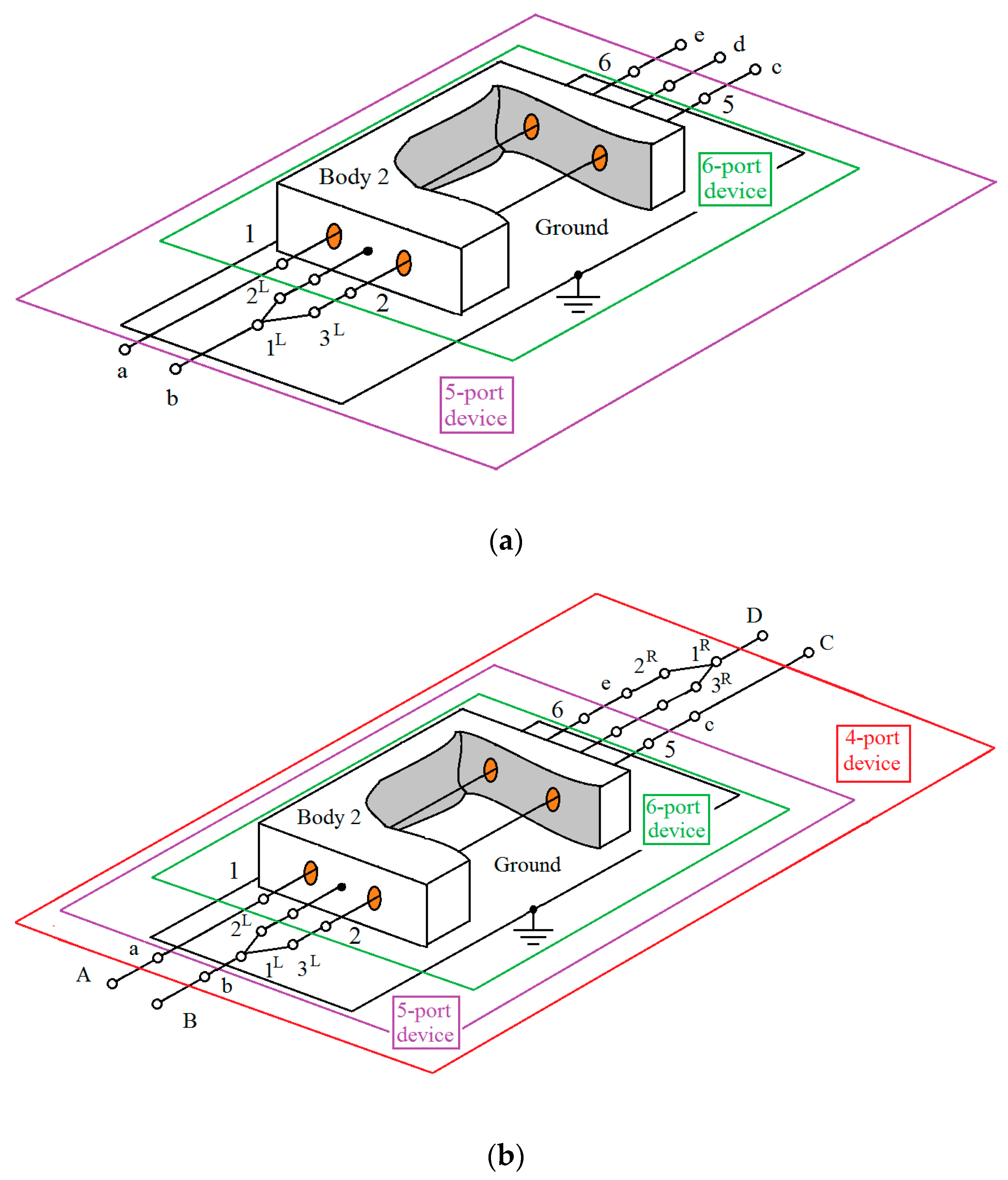
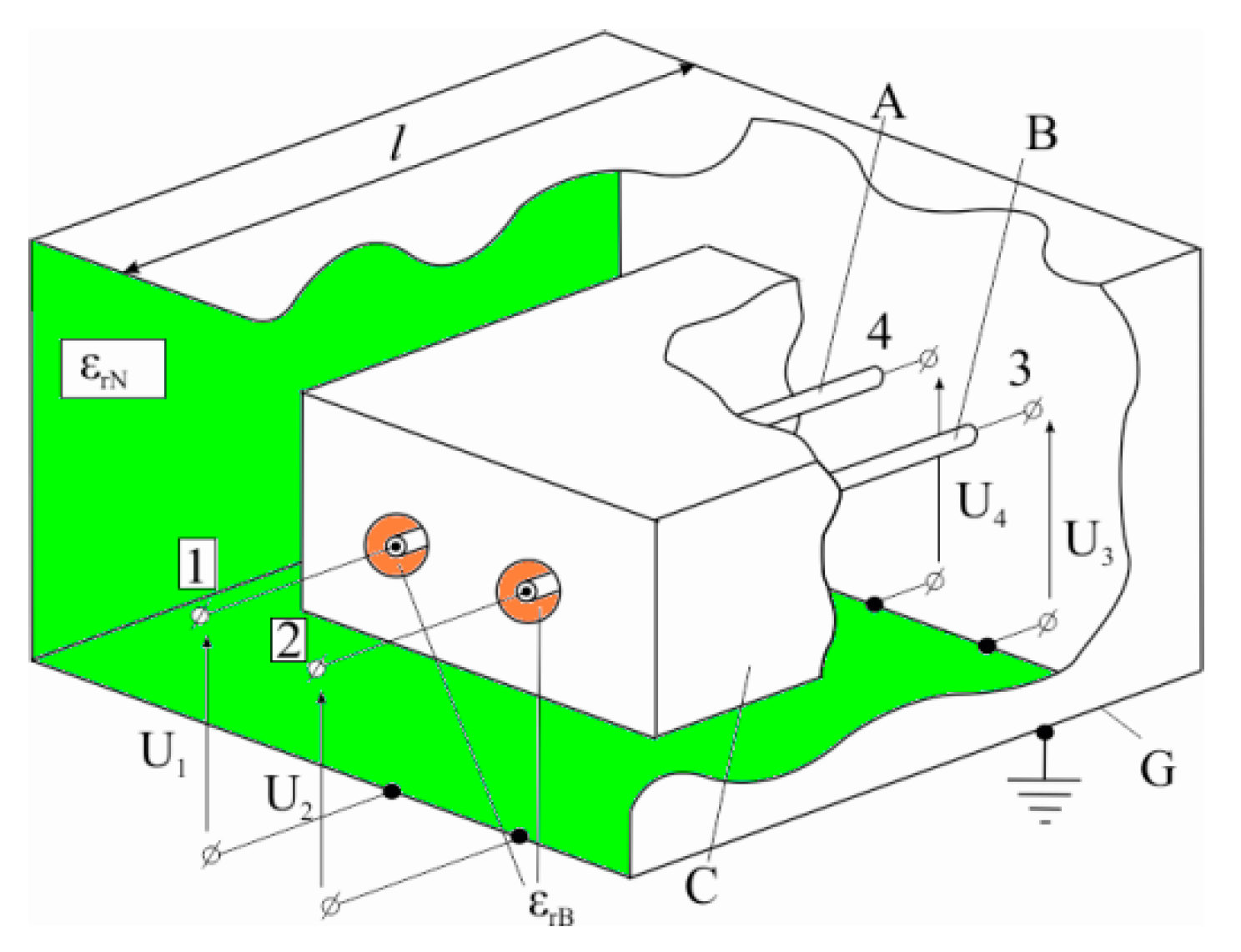
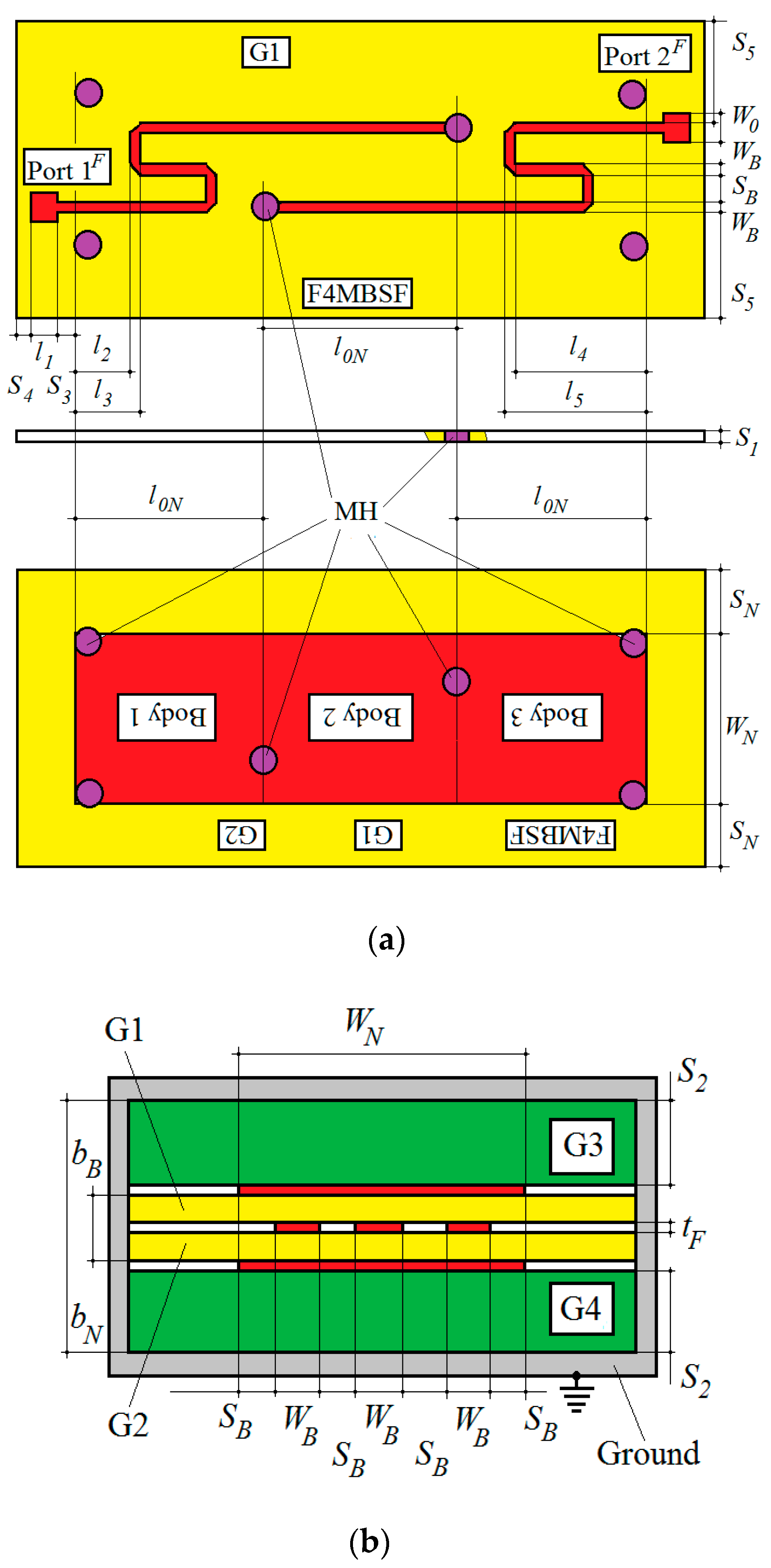
2. Basic Structure
3. Filter Design
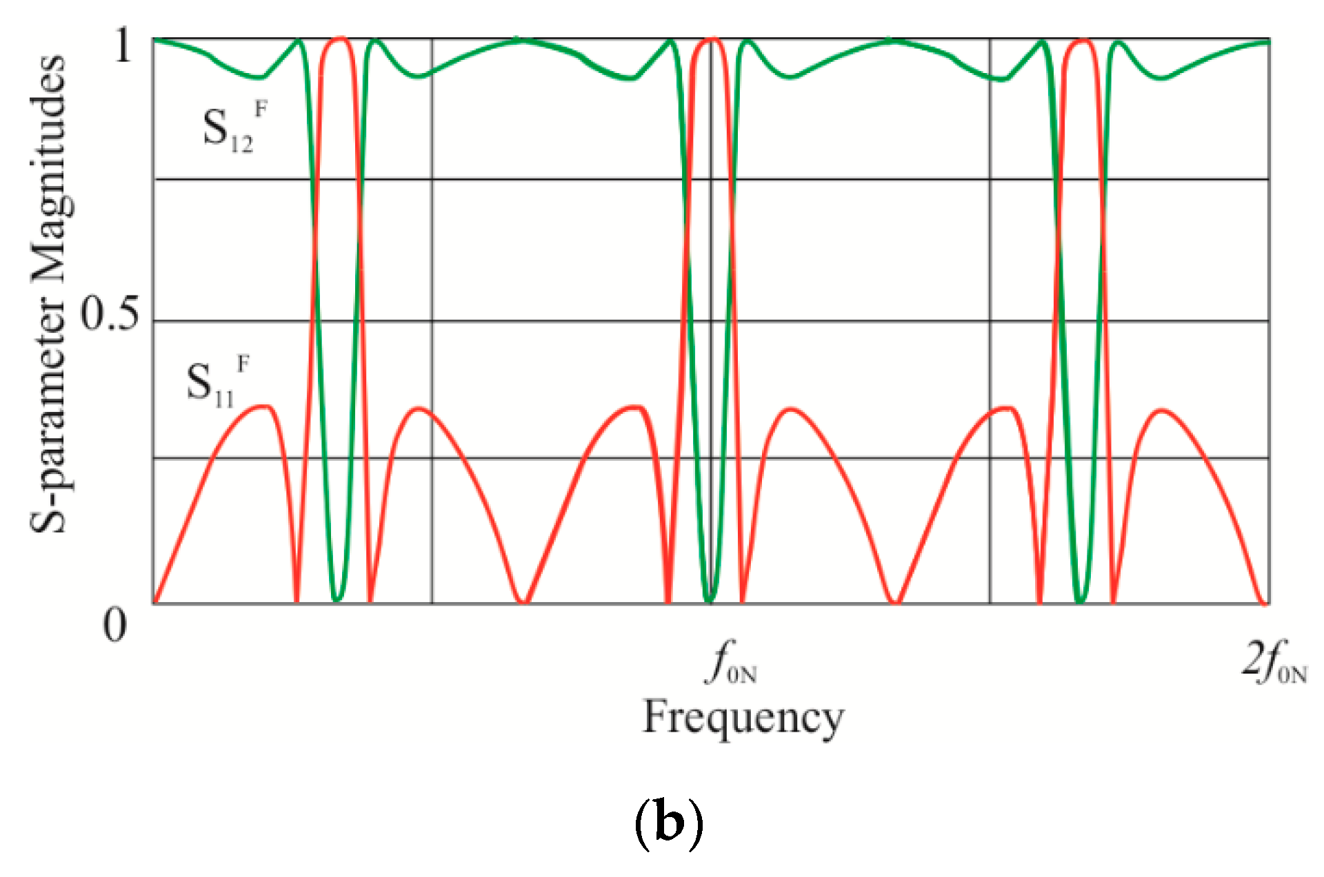
3.1. TEM Description of the Equivalent Filter Circuit
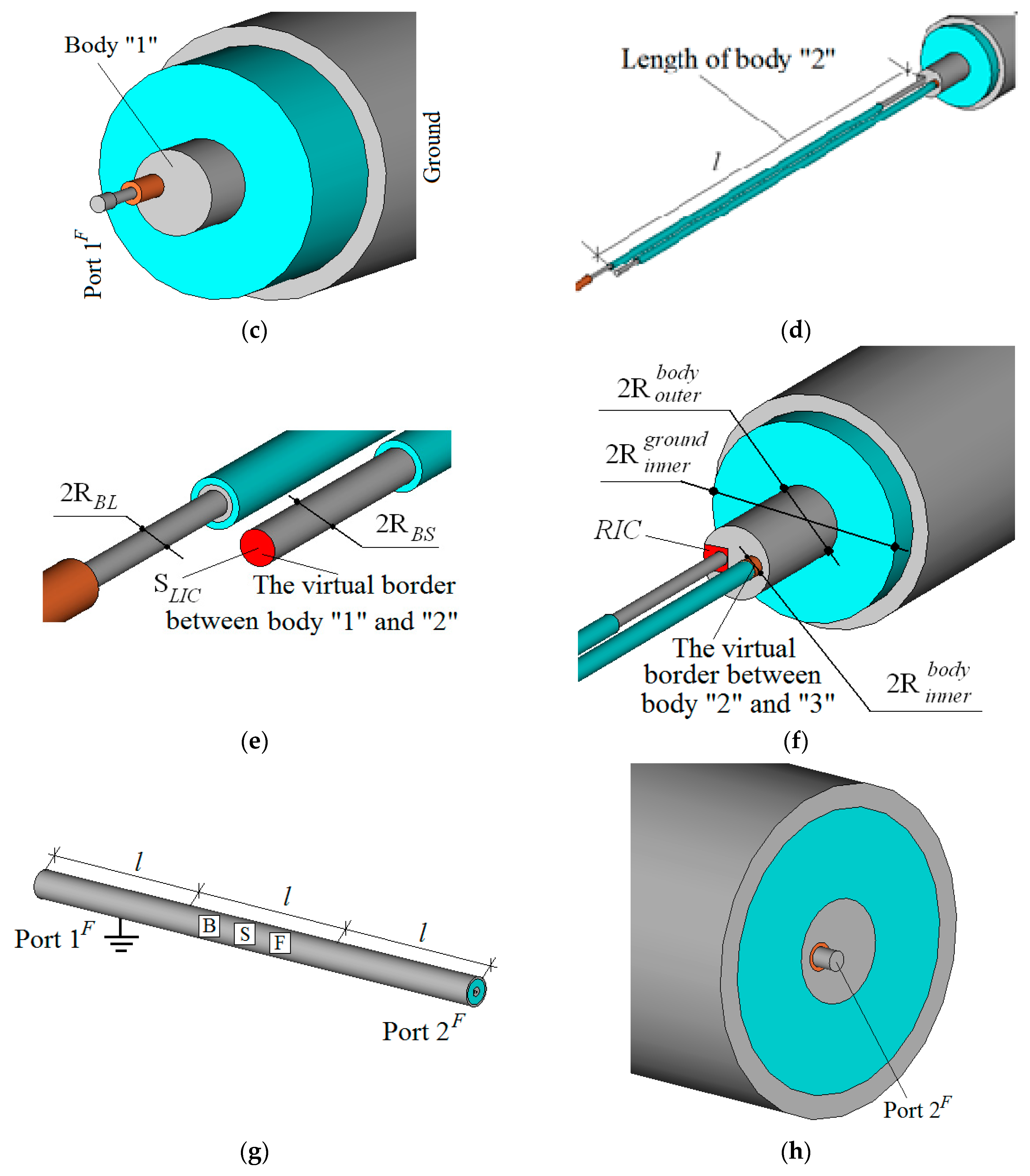
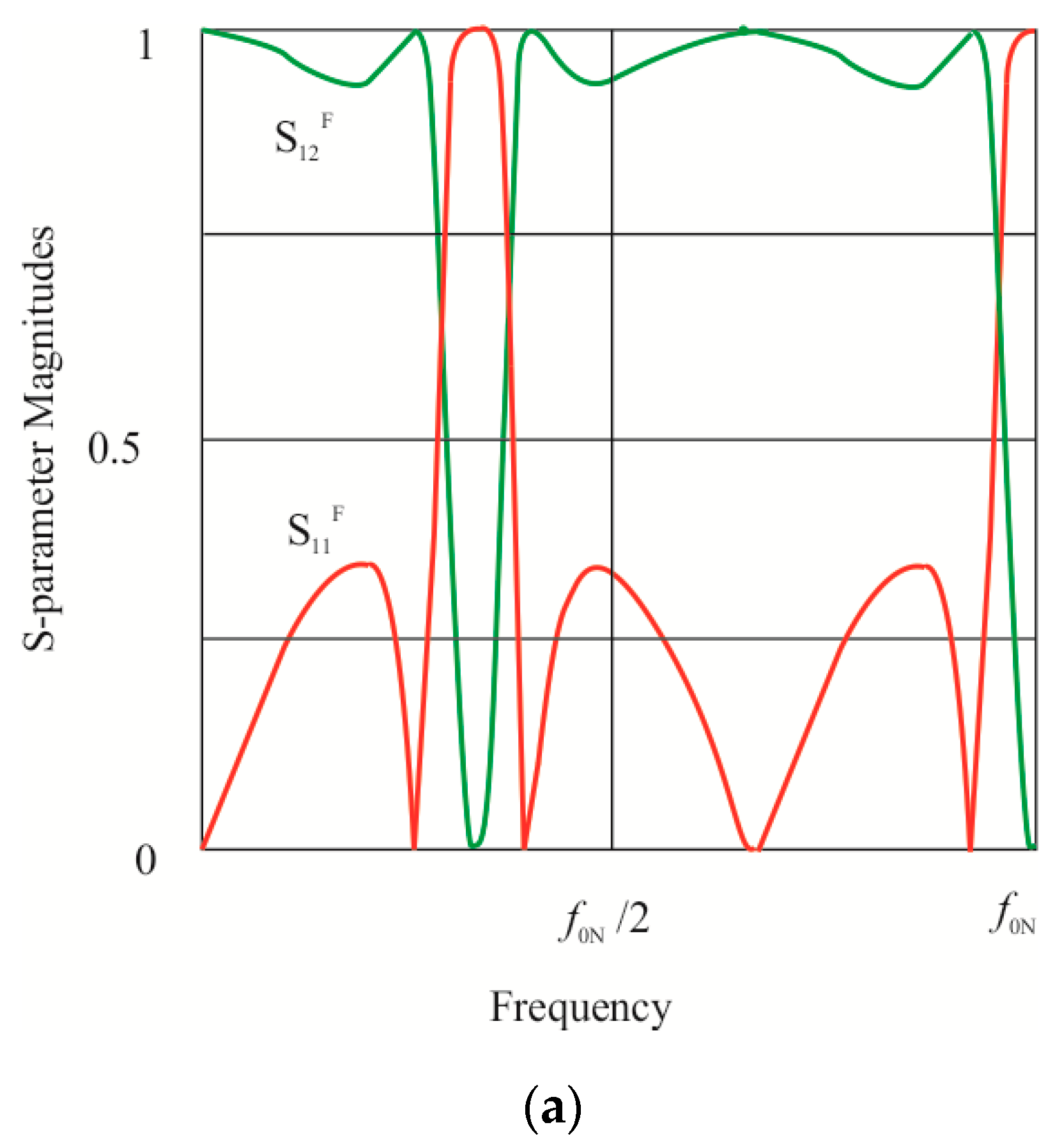
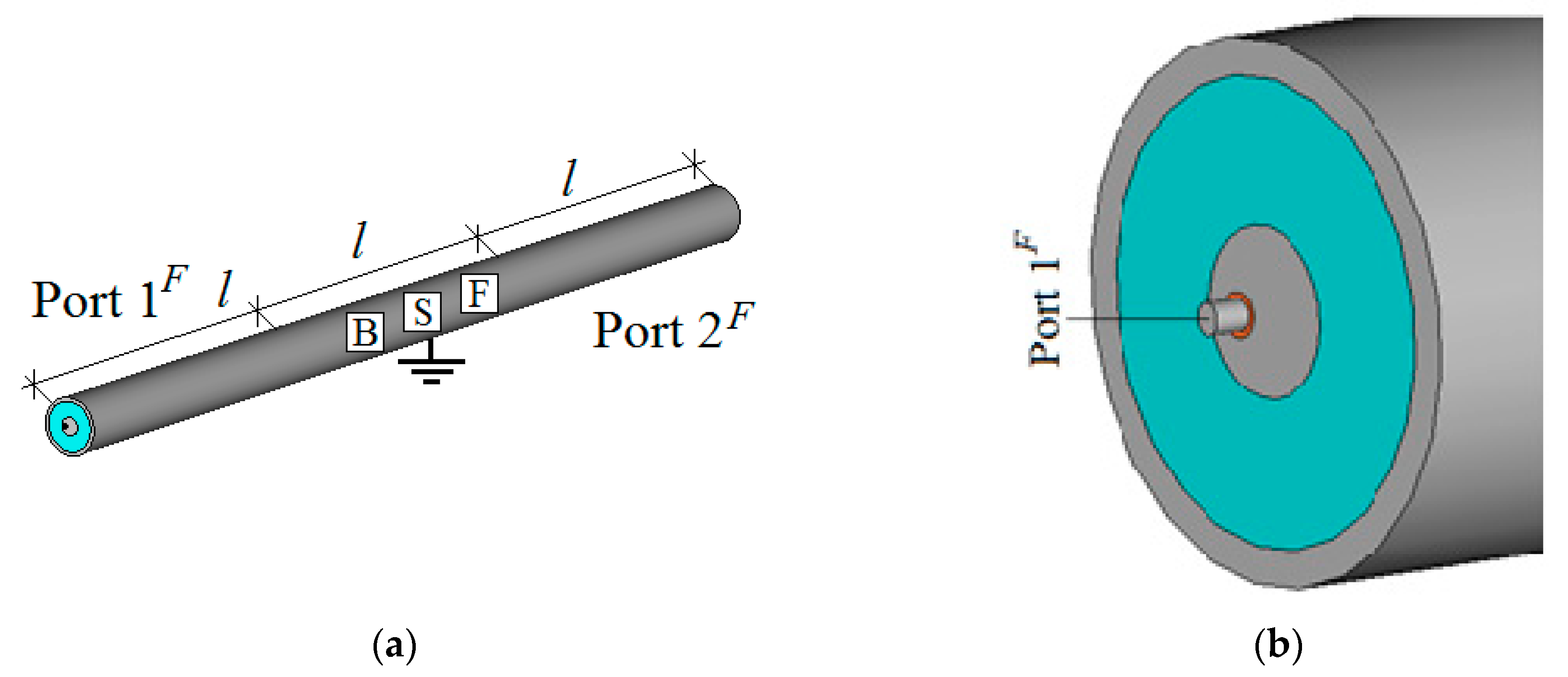
3.2. Full-Wave Simulations
- -
- the first halves of the solid metallic cylinders inside bodies “1” and “3” are surrounded by the orange medium with relative dielectric constant 4: 0.308 mm;
- -
- the second halves of the solid metallic cylinders inside body “2” are surrounded by the green vacuum filling: 0.43mm;
- -
- the inner radius of both solitary holes inside the solid cylinder with a floating potential that plays the role of all three bodies “1”, “2”, and “3” correspondingly connected in echelon: 0.6 mm, i.e., for 4 (orange medium) and 1 (green one) we have 20 Ω;
- -
- the outer radius of the cylinder with a floating potential: 2.205 mm;
- -
- the inner radius of a grounded cylinder related to all the three bodies: 6 mm, i.e., for 1 (green medium) we have 60 ;
- -
- the outer radius of the grounded cylinder is chosen as 7 mm.
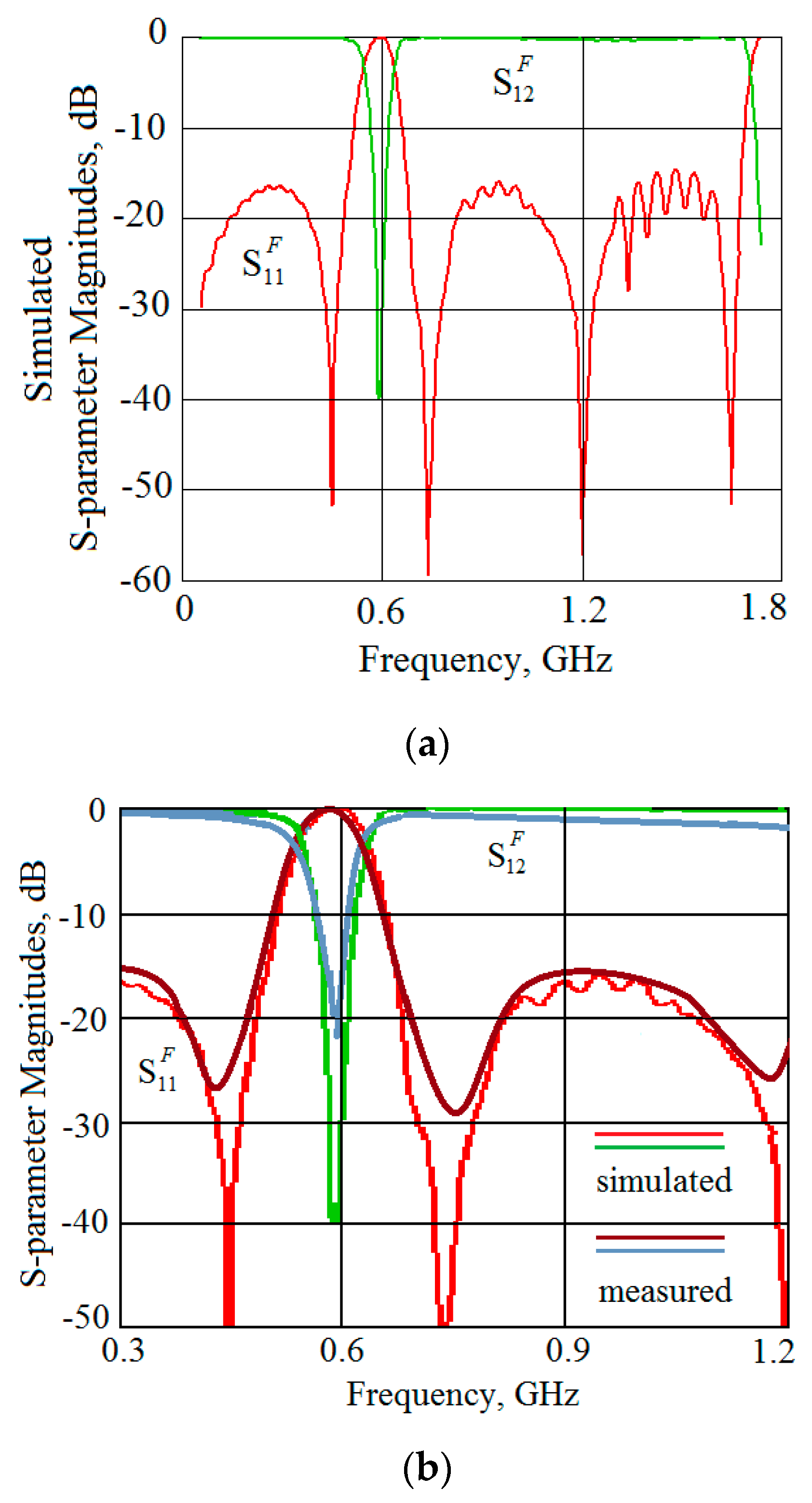
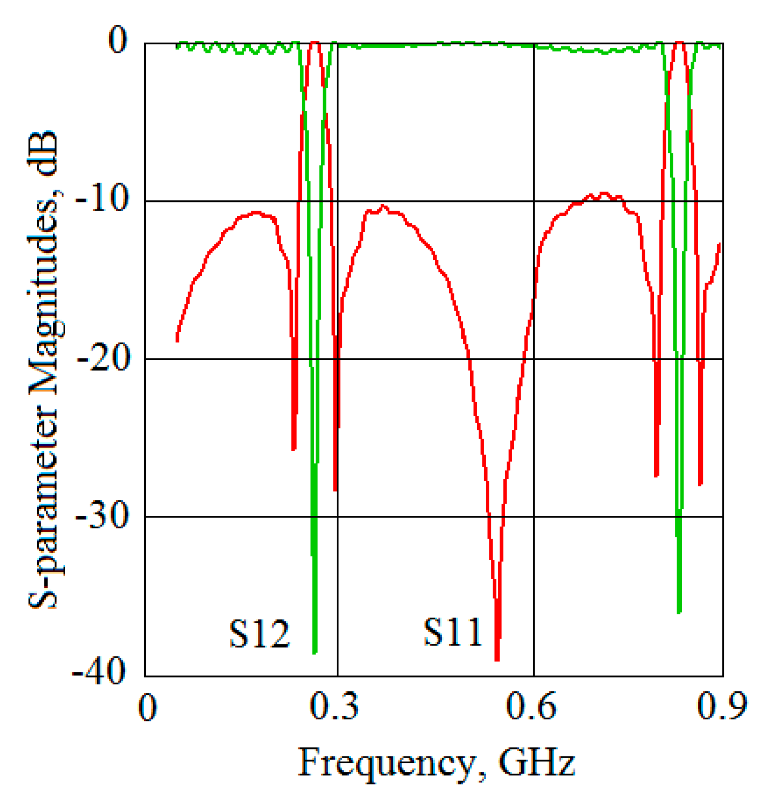
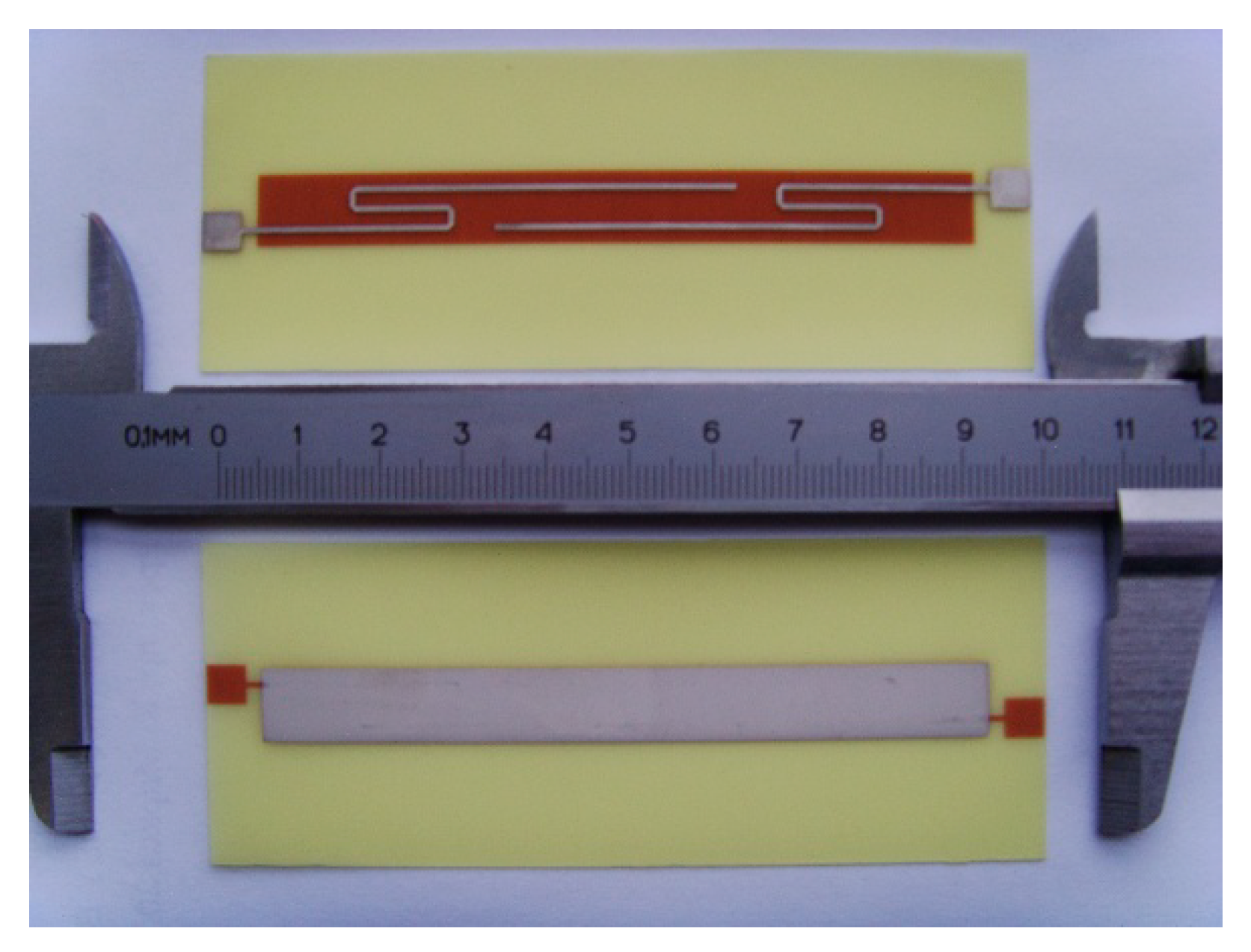
4. Experimental Results
- -
- the impedances 47 Ω are realized as the relative thin metallic bar of width and height 0.3 mm placed symmetrically between the ground planes with cross-sectional distance , as shown in Figure 6b;
- -
- the impedances 20 Ω are realized as the regular strip lines of thickness and width placed symmetrically between the ground planes with the common distance 0.26 mm.
5. Discussion
6. Conclusions
Author Contributions
Funding
Conflicts of Interest
Appendix A

References
- Hong, J.-S. Microstrip Filters for RF/Microwave Applications, 2nd ed.; Chang, K., Ed.; Wiley: Hoboken, NJ, USA, 2011. [Google Scholar]
- Levy, R.; Cohn, S.B. A history of microwave filter research, design, and development. IEEE Trans. Microw. Theory Tech. 1984, 32, 1055–1067. [Google Scholar] [CrossRef]
- Levy, R. Classic Works in RF Engineering, Volume 2, Microwave and RF Filters; Artech House: Norwood, MA, USA, 2007. [Google Scholar]
- Mongia, R.K.; Bahl, I.J.; Bhartia, P.; Hong, J. RF and Microwave Coupled-Line Circuits; Artech House: Norwood, MA, USA, 2007. [Google Scholar]
- Matthaei, G.L.; Young, L.; Jones, E.M.T. Microwave Filters, Impedance Matching Networks and Coupling Structures; McGraw-Hill: New York, NY, USA, 1964. [Google Scholar]
- Hao, Z.-C.; Hong, J.-S. Ultrawideband filter technologies. IEEE Microw. Mag. 2010, 11, 56–68. [Google Scholar] [CrossRef]
- Cameron, R.J.; Yu, M.; Wang, Y. Direct-coupled microwave filters with single and dual stopbands. IEEE Trans. Microw. Theory Tech. 2005, 53, 3288–3297. [Google Scholar] [CrossRef]
- Levy, R.R.; Snyder, V.; Shin, S. Bandstop filters with extended upper passbands. IEEE Trans. Microw. Theory Tech. 2006, 54, 2503–2515. [Google Scholar] [CrossRef]
- Shaman, H.; Hong, J.-S. Wideband bandstop filter with cross-coupling. IEEE Trans. Microw. Theory Tech. 2007, 55, 1780–1785. [Google Scholar] [CrossRef]
- Chin, K.-S.; Yeh, J.-H.; Chao, S.-H. Compact dual-band bandstop filters using stepped-impedance resonators. IEEE Microw. Wireless Compon. Lett. 2007, 17, 849–851. [Google Scholar] [CrossRef]
- Mandal, M.K.; Divyabramham, K.; Sanyal, S. Compact, wideband bandstop filters with sharp rejection characteristic. IEEE Microw. Wirel. Compon. Lett. 2008, 18, 665–667. [Google Scholar] [CrossRef]
- Fathelbab, W.M. Two novel classes of band-reject filters realizing broad upper pass bandwidth—Synthesis and design. IEEE Trans. Microw. Theory Tech. 2011, 59, 250–259. [Google Scholar] [CrossRef]
- Mandal, M.K.; Divyabramham, K.; Velidi, V.K. Compact wideband bandstop filter with five transmission zeros. IEEE Microw. Wirel. Compon. Lett. 2012, 22, 4–6. [Google Scholar] [CrossRef]
- Xiao, J.-K.; Zhu, Y.-F. Multi-band bandstop filter using inner T-shaped defected microstrip. AEU Int. J. Electron. Commun. 2014, 68, 90–96. [Google Scholar] [CrossRef]
- Atuchin, V.V.; Buhtiyarov, D.A.; Gorbachev, A.P. Compact printed microwave filters for wireless communication applications. Pac. Sci. Rev. A Nat. Sci. Eng. 2016, 18, 157–161. [Google Scholar] [CrossRef]
- Koirala, G.R.; Shrestha, B.; Kim, N.-Y. Compact dual-wideband bandstop filter using a stub-enclosed stepped-impedance resonator. AEU Int. J. Electron. Commun. 2016, 70, 198–203. [Google Scholar] [CrossRef]
- Gupta, S.C.; Kumar, M.; Meena, R.S. Design & analysis of a microstrip line multi band UWB filter. AEU Int. J. Electron. Commun. 2016, 70, 1556–1564. [Google Scholar]
- Ebrahimi, A.; Withayachumnankul, W.; Al-Sarawi, S.F.; Abbott, D. Compact second-order bandstop filter based on dual-mode complementary split-ring resonator. IEEE Microw. Wirel. Compon. Lett. 2016, 26, 571–573. [Google Scholar] [CrossRef]
- Min, X.; Zhang, H. Compact triple-band bandstop filter using folded, symmetric stepped-impedance resonators. AEU Int. J. Electron. Commun. 2017, 77, 105–111. [Google Scholar] [CrossRef]
- Feng, W.J.; Hong, M.L.; Che, W.Q.; Xue, Q. Dual-band microstrip bandstop filter with multiple transmission poles using coupled lines. IEEE Microw. Wirel. Compon. Lett. 2017, 27, 236–238. [Google Scholar] [CrossRef]
- Atuchin, V.V.; Gorbachev, A.P.; Khrustalev, V.A.; Tarasenko, N.V. Reentrant wideband quasi-elliptical bandpass filter. J. Electromagn. Waves Appl. 2018. [Google Scholar] [CrossRef]
- Cohn, S.B. The re-entrant cross section and wide-band 3-dB hybrid couplers. IEEE Trans. Microw. Theory Tech. 1963, 11, 254–258. [Google Scholar] [CrossRef]
- Lavendol, L.; Taub, J.J. Re-entrant directional coupler using strip transmission line. IEEE Trans. Microw. Theory Tech. 1965, 13, 700–701. [Google Scholar] [CrossRef]
- Cristal, E.G. Re-entrant directional couplers having direct coupled center conductors. IEEE Trans. Microw. Theory Tech. 1966, 14, 207–208. [Google Scholar] [CrossRef]
- Cristal, E.G. Nonsymmetrical coupled lines of reentrant cross section. IEEE Trans. Microw. Theory Tech. 1967, 15, 529–530. [Google Scholar] [CrossRef]
- Cristal, E.G. Correction to “Nonsymmetrical coupled lines of reentrant cross section”. IEEE Trans. Microw. Theory Tech. 1968, 16, 57. [Google Scholar] [CrossRef]
- Gill, P.E.; Murray, W.; Wright, M.H. Practical Optimization; Academic Press: London, UK, 1981. [Google Scholar]
- Gorbachev, A.P.; Potryasov, I.I. Designing microwave devices with shielded elements. J. Commun. Technol. Electron. 2000, 45, 462–466. [Google Scholar]
- Gorbachev, A.P.; Tarasenko, N.V. The novel reentrant power splitters and bandstop elliptic filters. In Proceedings of the 2016 13th International Scientific-Technical Conference on Actual Problems of Electronics Instrument Engineering (APEIE), Novosibirsk, Russia, 3–6 October 2016; pp. 173–176. [Google Scholar]
- Atuchin, V.V.; Gorbachev, A.P.; Khrustalev, V.A.; Tarasenko, N.V. The dual-band reentrant power splitter. AEU Int. J. Electron. Commun. 2018, 84, 21–26. [Google Scholar] [CrossRef]
- Jones, E.M.T.; Bolljahn, J.T. Coupled-strip-transmission-line filters and directional couplers. IEEE Trans. Microw. Theory Tech. 1956, 4, 75–81. [Google Scholar] [CrossRef]
- Frickey, D.A. Conversions between S, Z, Y, h, ABCD,and T parameters which are valid for complex source and load impedances. IEEE Trans. Microw. Theory Tech. 1994, 42, 205–211. [Google Scholar] [CrossRef]
- Cameron, R.J.; Kudsia, C.M.; Mansour, R.R. Microwave Filters for Communication Systems: Fundamentals, Design and Applications; Wiley: Hoboken, NJ, USA, 2007. [Google Scholar]
- Otoshi, T.Y. On the scattering parameters of a reduced multiport. IEEE Trans. Microw. Theory Tech. 1969, 17, 722–724. [Google Scholar] [CrossRef]
- Monaco, V.A.; Tiberio, P. Computer-aided analysis of microwave circuits. IEEE Trans. Microw. Theory Tech. 1974, 22, 249–263. [Google Scholar] [CrossRef]
- Kolundzija, B.M.; Ognjanovic, J.S.; Sarkar, T.K. WIPL-D: Microwave Circuit and 3D EM Simulation for RF & Microwave Applications, Software and User’s Manual; Artech House: Norwood, MA, USA, 2005. [Google Scholar]
- Bakharev, S.I.; Volman, V.I.; Lib, Y.N.; Mamonova, N.; Muravtcov, A.; Sarkisjantc, A.; Silin, R.; Slavinsky, O.; Shirjaev, D. Handbook on Design of Microwave Circuits; Radio & Swjaz: Мoscow, Russia, 1982. (In Russian) [Google Scholar]
- Alekseev, V.G.; Gridnev, V.N.; Nesterov, Y.I.; Filin, G. Technology of Digital Electronic Devices, Equipment and Automation; Wisshaya Shkola: Moscow, Russia, 1984. (In Russian) [Google Scholar]
- Gorbachev, A.P. The reentrant wide-band directional filter. IEEE Trans. Microw. Theory Tech. 2002, 50, 2028–2031. [Google Scholar] [CrossRef]
- Gorbachev, A.P.; Malinko, D.A.; Vasilenko, A.A. The reentrant wideband bandpass/bandstop elliptic filters. In Proceedings of the 2010 10th International Conference on Actual Problems of Electronic Instrument Engineering APEIE-2010, Novosibirsk, Russia, 22–24 September 2010; pp. 56–63. [Google Scholar]
- Gorbachev, A.P.; Churkin, V.S.; Vasilenko, A.A. The modified Schiffman phase shifter. In Proceedings of the 2010 10th International Conference on Actual Problems of Electronic Instrument Engineering APEIE-2010, Novosibirsk, Russia, 22–24 September 2010; pp. 124–126. [Google Scholar]


© 2019 by the authors. Licensee MDPI, Basel, Switzerland. This article is an open access article distributed under the terms and conditions of the Creative Commons Attribution (CC BY) license (http://creativecommons.org/licenses/by/4.0/).
Share and Cite
Atuchin, V.V.; Gorbachev, A.P.; Khrustalev, V.A.; Tarasenko, N.V. The Reentrant Four-Layer Quasi-Elliptic Bandstop Filter. Electronics 2019, 8, 81. https://doi.org/10.3390/electronics8010081
Atuchin VV, Gorbachev AP, Khrustalev VA, Tarasenko NV. The Reentrant Four-Layer Quasi-Elliptic Bandstop Filter. Electronics. 2019; 8(1):81. https://doi.org/10.3390/electronics8010081
Chicago/Turabian StyleAtuchin, Victor V., Anatoly P. Gorbachev, Vladimir A. Khrustalev, and Natalya V. Tarasenko. 2019. "The Reentrant Four-Layer Quasi-Elliptic Bandstop Filter" Electronics 8, no. 1: 81. https://doi.org/10.3390/electronics8010081
APA StyleAtuchin, V. V., Gorbachev, A. P., Khrustalev, V. A., & Tarasenko, N. V. (2019). The Reentrant Four-Layer Quasi-Elliptic Bandstop Filter. Electronics, 8(1), 81. https://doi.org/10.3390/electronics8010081