Article

Design of High Frequency, Low Phase Noise LC Digitally Controlled Oscillator for 5G Intelligent Transport Systems

by
Vytautas Macaitis
* and
Romualdas Navickas
Micro and Nanoelectronics Systems Design and Research Laboratory, Vilnius Gediminas Technical University, 10257 Vilnius, Lithuania
*
Author to whom correspondence should be addressed.
Electronics 2019, 8(1), 72; https://doi.org/10.3390/electronics8010072
Submission received: 9 November 2018 / Revised: 18 December 2018 / Accepted: 3 January 2019 / Published: 8 January 2019
(This article belongs to the Section Circuit and Signal Processing)

Abstract

:
This paper presents the design, simulation, and measurements of a low power, low phase noise 10.25–11.78 GHz LC digitally controlled oscillator (LC DCO) with extended true single phase clock (E-TSPC) frequency divider in 130 nm complementary metal–oxide–semiconductor (CMOS) technology for 5G intelligent transport systems. The main goal of this work was to design the LC DCO using a mature and low-cost 130 nm CMOS technology. The designed integrated circuit (IC) consisted of two parts: the LC DCO frequency generation and division circuit and an independent frequency divider testing circuit. The proposed LC DCO consisted of the following main blocks: the high Q-factor inductor, switched-capacitors block, cross-coupled transistors, and the current control block. Inductors with switched-capacitors block formed an LC tank. The designed E-TSPC frequency divider consisted of eight blocks connected in a series; each block increased the division ratio by a factor of two. The frequency of the input signal was divided in the region from two to 256 times using the designed divider. The main parameters of the designed E-TSPC divider and the LC DCO measurements were given as follows: LC DCO achieved a wide tuning range from 10.25 GHz to 11.78 GHz (1.53 GHz, 15.28% bandwidth); phase noise at 1 MHz offset frequency from LC DCO lowest carrier frequency was −113.42 dBc/Hz; phase noise at 1 MHz offset frequency from LC DCO highest carrier frequency was −110.51 dBc/Hz; The average power consumption of the designed LC DCO core and E-TSPC divider were 10.02 mW and 97.52 mW, respectively; the figure of merit (FOM) and the extended FOMT values of the proposed LC DCO were −183.52 dBc/Hz and −187.20 dBc/Hz, respectively. These FOM and FOMT results were achieved due to very low phase noise (−113.52 dBc/Hz) and a wide frequency tuning range (15.28%). The total layout area including the pads was 1.5 mm × 1.5 mm, with the largest part of the layout occupied by the proposed LC DCO (193 µm × 311 µm). The largest part of the LC DCO was occupied by the inductor 184 µm × 184 µm. The manufactured chip was packed into a quad flat no-leads (QFN) 20 pads package.

1. Introduction

The automotive industry is evolving through interconnected and autonomous vehicles that bring reduced traffic congestion, reduced environmental impact, and reduced capital costs. Vehicle to everything (V2X) technology is the key to intelligent transportation systems (ITS) based on 5G wireless network evolution. The ITS combines many different types of information and communication technologies to create intelligent wireless networks. Such a smart ITS network is needed for reasons such as improving traffic safety (real-time weather monitoring, warning sign notifications, speed limitation, emergency alerts), reducing infrastructure damage (overloaded machines can be identified and eliminated from traffic participation, thus avoiding damage to the road), and traffic control (traffic management can be adaptive depending on traffic flow). These benefits of an ITS can make traffic safer, faster, and more convenient. To create an ITS network, transmitters are required that generate signals of a certain frequency using a frequency synthesizer based on the LC digitally controlled oscillator (LC DCO).
Most LC DCOs around 10 GHz are designed using 65 nm and newer technology, resulting in a significant increase in the cost of the final product. The used area of silicon is not reduced by much since most of the design is occupied by an inductor. The basic idea behind this article was to design a standard N-channel metal oxide semiconductor (NMOS) architecture, low power, low occupancy, low phase noise, wide tuning range—and most importantly—cheap DCO using low-cost 130 nm technology. The application of this low-cost DCO in the constantly evolving intelligent transport systems was the main goal. The main difficulty was getting the required parameters and performance using a mature low-cost 130 nm IBM radio frequency (RF) integrated circuit (IC) technology. High-quality RF transistors and high-quality factor Q copper inductors were used in this technology with correlating results of the simulations and measurements. In this technology, copper and aluminum wiring with a thick top metal was used. The 130 nm technology is a semiconductor technology for low-cost and high-performance wireless applications. Unfortunately, specific and more detailed information about this technology is under a non-disclosure agreement.
The aim of this work was to create an LC DCO whose output signal’s frequency range is suitable for USA and Japan 5G ITS bands. The LC DCO output signal frequency should correspond to the 2.5 LTE B24 and 600 MHz USA 5G band, as well as the —4.4–4.9 GHz Japan 5G band [1]. DCO may be used in other communication systems.
The LC DCO alone could not generate a stable frequency, thus additional blocks were used that collectively formed a digital or analog phase locked loop (PLL), which was applied in multiband multistandard radio frequency (RF) transceivers.
As one of the most important blocks of any wireless multiband, the multistandard transceiver is the PLL. The main PLL applications are signal synthesis, synchronization, modulation, demodulation, as well as signal tracking. There are two main types of PLLs: conventional PLL (CPLL) and all digital PLLs (ADPLL). The CPLLs main advantages are frequency synthesis with good performance and a high frequency range, but the disadvantages are the high power consumption and large chip area. ADPLLs are characterized by low power consumption, small area, and scalability across different technology nodes. The blocks of these PLLs are presented in the following paragraphs.
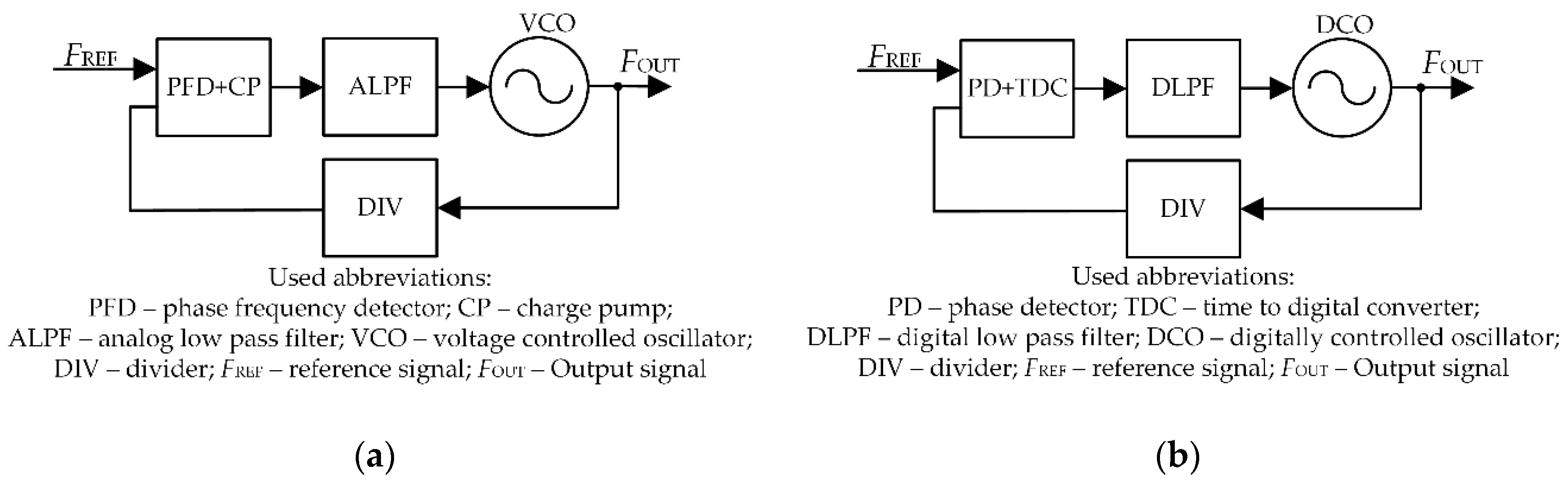
The basic PLL block diagram is shown in Figure 1a. In a typical PLL, a voltage controlled oscillator (VCO) generates unstable output signal frequency FOUT. The transceiver cannot function properly when the frequency of the generated signal is unstable, thus an additional reference signal (FREF) is used to stabilize the frequency. The FOUT adjustment is as follows: the feedback divider (DIV) generates a comparison frequency using the VCO output signal FOUT divided by coefficient N; phase frequency detector (PFD) compares the phase/frequency of two signals with frequencies FREF and FOUT/N at its input. The purpose of the PFD is to detect the phase difference between FREF and FOUT/N. It is considered that the PLL is locked when the FREF signal is equal to the signal FOUT/N. The main purpose of a charge pump (CP) is to convert the logic states of the phase frequency detector into analog signals suitable to control the VCO. The output of the charge pump is connected to an analog low pass filter (ALPF) that integrates the charge pump output current to an equivalent VCO control voltage [2].
The basic ADPLL synthesizer block diagram is shown in Figure 1b. In the digital controlled oscillator, DCO replaces the VCO. The time-to-digital converter (TDC) with the phase detector (PD) replaces the phase frequency detector and the charge-pump of the ADPLL. The digital low pass filter (DLPF) replaces the analog low pass filter of the PLL. The main advantages of the ADPLL are less chip area, elimination of additional external control voltage (mostly, the ALPF is realized on the printed circuit board (PCB) side, the DLPF is integrated inside the chip), the chip cost is lower, and, with digitalized block controls, all system programming is simplified [3]. The main advantages of LC DCO versus LC VCO are the lower occupied area, lower phase noise, lower power consumption, and the ability to digitize further deployable systems. The following paragraphs outline the main architectures of LC DCO.
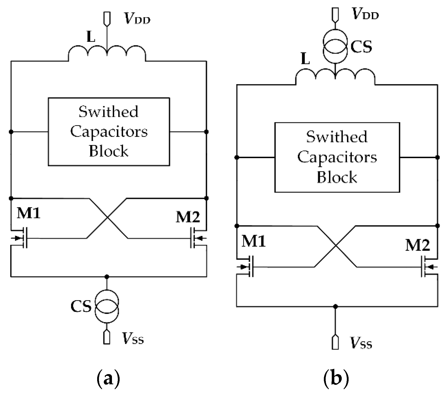
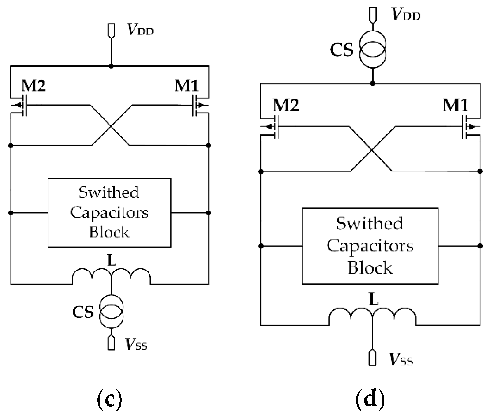
The basic architectures of N-channel metal oxide semiconductor (NMOS) LC DCO cores are presented in Figure 2a,b. The current source connected to the ground architecture (Figure 2a) has the lowest sensitivity to noise on the ground line but the highest sensitivity to power supply source noise. This architecture is characterized by lower flicker noise in the output compared to architecture, as shown in Figure 2b. This is achieved due to a more correct output signal waveform. Reduced flicker noise causes lower distortion of the output signal. Using this architecture’s output signal swing can be doubled compared to the used supply voltage and can be used for phase noise reduction [4].
The basic architectures of P-channel metal oxide semiconductor (PMOS) LC DCO cores are presented in Figure 2b,c. In order to obtain the same operating frequency, a PMOS-based LC DCO core would require a transistor that is twice as large as the one in an NMOS-based LC DCO core. This increases both the occupied chip area and the power consumption but improves phase noise due to the lower PMOS transistor flicker noise in comparison to that of NMOS devices.
Hybrid NMOS and PMOS transistor architectures are also possible. Such architecture consists of a PMOS transistor pair connected to the power supply while an NMOS transistors pair is connected to the ground. This results in two pairs of transistors, allowing half of the energy to be consumed by the same negative resistance. This architecture receives output swing close to the supply voltage, thus the generated signal is limited by the voltage supply, which depends on the technology of the integrated circuits. With a low output signal swing, the phase noise gets worse and further signal processing becomes more complex.
We decided to use the Figure 2a LC DCO design architecture with an NMOS LC DCO core when the current source (CS) connected to the ground in order to fulfill the requirements of reducing the occupied space but maintaining a double output signal voltage swing when compared to the supply voltage (the signal generated by the LC DCO is processed by other blocks). The LC DCO’s operating frequency is high, around 10 GHz, as NMOS transistors are faster than the PMOS, thus a higher frequency can be achieved when using NMOS architecture.
A previous work titled “CMOS Technology based LC VCO Review” contains a review and a comparison of 44 different LC oscillators published in papers [5]. In order to quantify the comparison of the latter LC oscillators, an FOMT was used. According to the acquired LC oscillators FOMT results, the best overall performance was achieved when the circuit was implemented in the 130 nm CMOS process, and the second best was achieved when using the 65 nm CMOS process. Therefore, in order to design an LC DCO with low phase noise, low power consumption, and wide tuning range while also reducing the overall price, the 130 nm CMOS process was chosen.

2. Design of the LC DCO and Frequency Divider

The simplified block diagram of the proposed LC DCO and frequency divider is presented in Figure 3. The block diagram consisted of the following components: LC tank based DCO, frequency divider, and output buffer. The designed IC consisted of two parts: the LC DCO frequency generation and division circuit and an independent frequency divider testing circuit. Due to the limited number of IC package pads, only two divider outputs (division by 64 and 256) were connected to be measured externally. In order to check the frequency divider separately, it was included as an independent block but with different division ratios (division by 16 and 32) [6].

2.1. LC Core Based DCO

The schematic of the proposed LC DCO is shown in Figure 4. The proposed DCO consisted of these main blocks: the highest available Q-factor inductor (L)—which was dependent on IC technology, a switched-capacitors block, cross-coupled transistors (M1, M2), and the current control block. The inductor with a switched-capacitors block formed an LC tank. Under real conditions, the generated signal in this circuit would be suppressed. To avoid this effect, the NMOS M1 and M2 transistors were connected to the circuit. They created a negative resistance to eliminate LC tank losses so that the circuit could generate constant fluctuations.
The size of the cross-coupled transistors M1 and M2 were chosen so that the output signal’s swing would be not less than the supply voltage. With such a level of output signal, successful further signal processing was possible. The sizes of the cross-coupled transistors are presented in the table in Figure 4.

2.1.1. Switched-Capacitor Block

Frequency tuning was performed by changing the effective capacitance of the switched-capacitor block. The frequency was gradually changed by activating or deactivating arrays of certain size capacities. In this design, a 6-bit switched-capacitor array was used where each segment was controlled independently and could be toggled to reach the required capacity. All En bit (zero to five) switches in the proposed LC DCO were implemented as NMOS transistors.
The DCO tuning capacitance not only consisted of a switched-capacitors block to change the oscillator frequency, but it also included the parasitic capacitances. The main parasitic capacitances and blocks that affected the DCO frequency were the capacitances of the inductor, the active elements, and any load connected to the DCO output. Therefore, the computer simulations were carried out to calculate the exact sizes of the transistors of the switched-capacitors block. The sizes of the transistors used in this block are presented in Figure 4.
The above mentioned NMOS transistors drains and sources were shorted, which acted as one pin of the capacitor as the gate acted as another pin of the capacitor. Controls of the switched-capacitor block were routed to the chip output, thus the number of control bits was limited by the number of chip pads. There were only six pads left for this purpose since the other pads were used for the connection of input and output signals to supply voltage and ground. This resulted in 64 (26) different DCO control values. To control the frequency more precisely, an additional switched-capacitor block with smaller capacitance transistors could be used.

2.1.2. Current Control Block

The current control block was of high importance in the proposed DCO and was used for LC DCO core current regulation. The swing of the DCO output signal varied, so this block was intended to optimize swing within the normal range. This block could adjust LC DCO power consumption to the optimum and had a current mirror as the base element [7]. The sizes of the current control transistors M3 and M4 were chosen in such a way that the output current was double that of the control current. The sizes of the current control transistors are presented in the table in Figure 4.

2.1.3. Frequency Divider

A large part of the overall PLL synthesizer power consumption was drained by the frequency divider. True single phase clock (TSPC) dividers used lower power compared to the current mode logic (CML) frequency divider, but the main disadvantage of the TSPC was limited operating frequency. However, with the advancement of CMOS technology, the TSPC working frequency increased significantly. Extended TSPC (E-TSPC) designs were superior to the TSPC structure because E-TSPC flip-flops were utilized, which contained six transistors and were suitable for high frequency operation with low power consumption [8].
The circuit of the divide by two (N/2) stage is shown in Figure 5a. The circuit operated in two modes: pre-charge and evaluation. In the pre-charge mode—and before the operation of the falling edge of the clock (CLK pin)—the clock was in high state and the output (OUT pin) was in low state. The node N2 was pre-charged in low state, and when the ratio of M1 was greater than M2, N1 had a high value. M2 and M4 were in the cut area in the falling edge of clock. M1 was still connected, thus the output OUT charged more rapidly than node N2, and M2 remained in the cut area. In the pre-charge mode, node N2 had the low state and node OUT had the high state. In the evaluation mode, M2 and M3 were connected on the rising edge of the clock. Both M3 and M4 were connected and operated in the triode region, and the node N1 discharged rapidly and subsequently turned M3 on [9]. The proposed divider consisted of eight series connected blocks (each block increased the dividing factor by two). The proposed divider allowed division of the frequency of the input signal from two to 256 times. (Figure 5b). The ETSPC divider consisted of three transistors branches. The output level of the branch was determined by the ratio of PMOS and NMOS transistor sizes. This meant that static power dissipation existed in the ETSPC flip-flops. Transistor sizes were selected so that the divider used low power without affecting the operation of itself. The sizes of the transistors used in this block are presented in the table in Figure 5a [10].

3. Simulation and Measurements

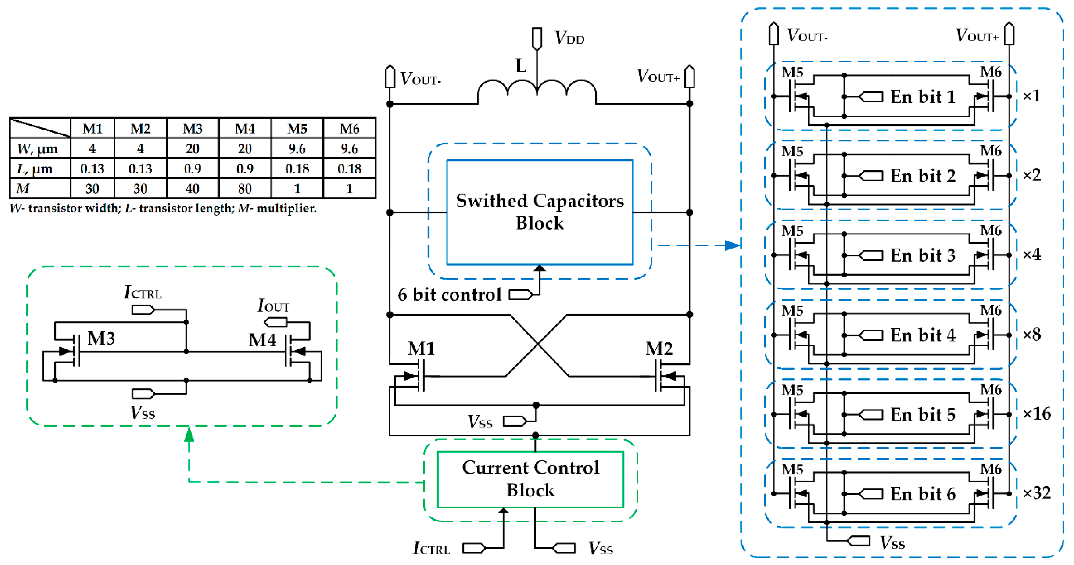
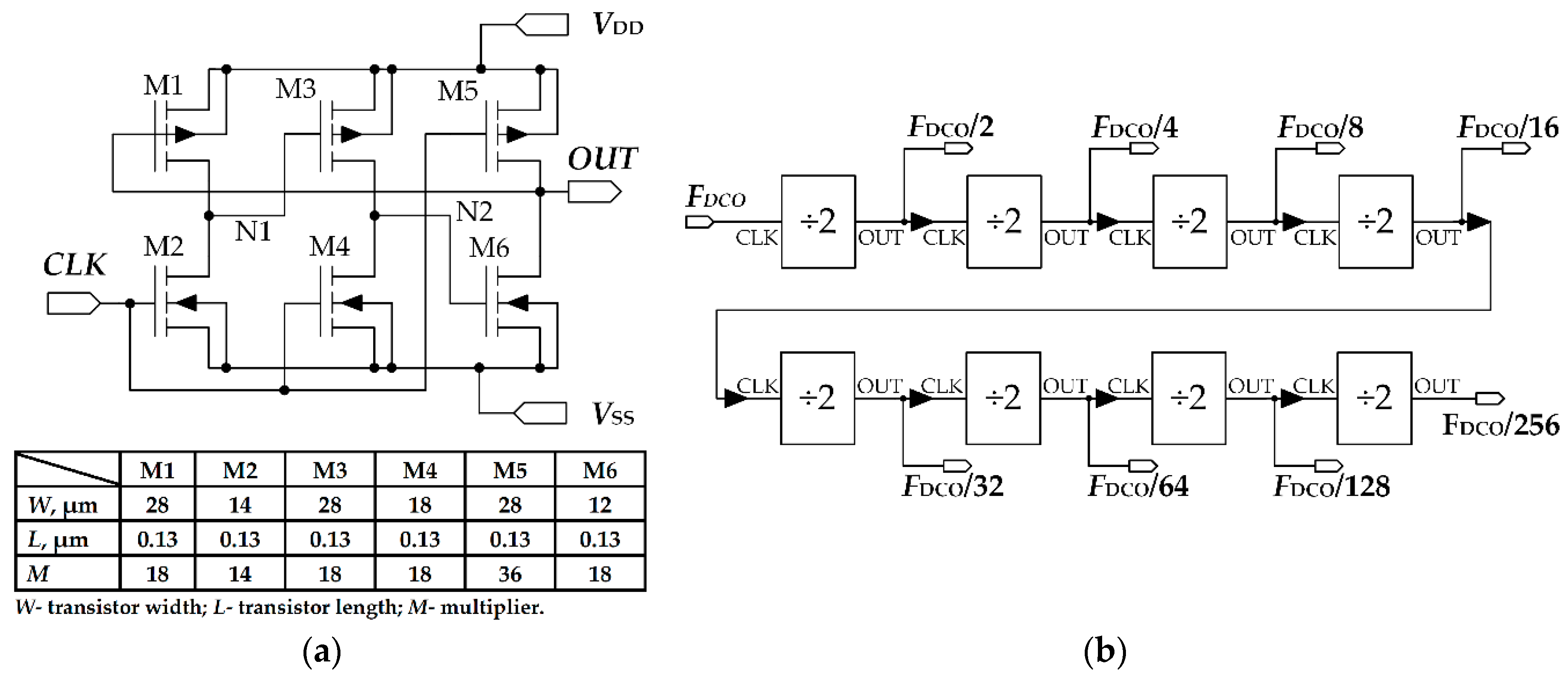
The proposed LC-DCO and frequency divider were designed in 130 nm RF CMOS technology in the Cadence IC software package. The design and simulation process was as follows. Firstly, a basic electrical schematic was designed and its simulations were carried out. The schematic was adjusted if the results obtained after the simulations did not meet the required conditions. Upon obtaining the required results, layout design was performed. Parasitics were extracted from the designed layout, then simulation of the layout was performed. In the absence of the required results, the electric schematic and layout were once again corrected, the layout was extracted, and simulations were performed. After obtaining the required simulation results, the main blocks were connected, which were also connected to the pads. After these steps, the whole system was verified. After making the chip, the basic parameters were measured and compared with the parameters obtained during the simulation. Simulations were performed in nominal conditions using 1.8 V supply voltage and 40 °C temperature. The main parameters of the simulations and measurements are presented in Table 1.
To evaluate the overall performance of the frequency oscillators, an FOM (1) and FOMT (2), including the tuning range, was used:
F O M = P N ( Δ f ) 20 log ( F 0 Δ f 10 ) + 10 log ( P 1 m W ) ,
F O M T = P N ( Δ f ) 20 log ( F 0 Δ F Δ f 10 ) + 10 log ( P 1 m W ) ,
where PNf) is the phase noise at an offset frequency Δf, F0 is the carrier frequency, P is the power consumption in mW, and ΔF is a percentage of the frequency tuning range [5]. The proposed LC DCO and E-TSPC divider schematics, post-layout, and chip main parameters are presented in Table 1.
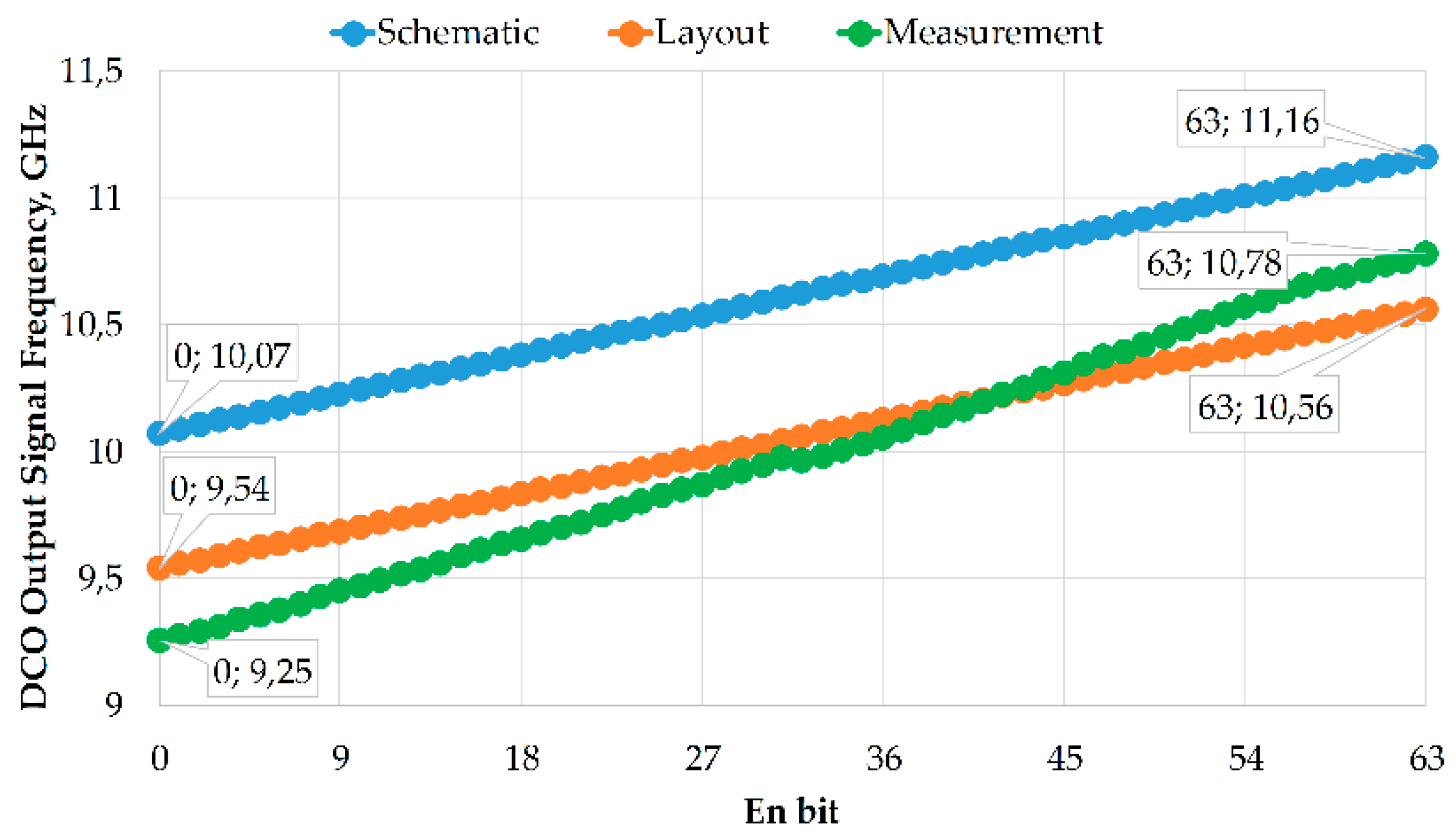
Figure 6 describes the tuning range of the proposed LC DCO. The LC DCO achieved a wide tuning range from 10.07 GHz to 11.16 GHz during schematic simulations. The tuning range reduced to 9.54–10.56 GHz during the post-layout simulation. The measured tuning range was 9.25–10.78 GHz, which was better than both the schematic and the post-layout simulation, and reached a 1.53 GHz bandwidth, which was 0.51 GHz wider than the results obtained in the post-layout simulation.
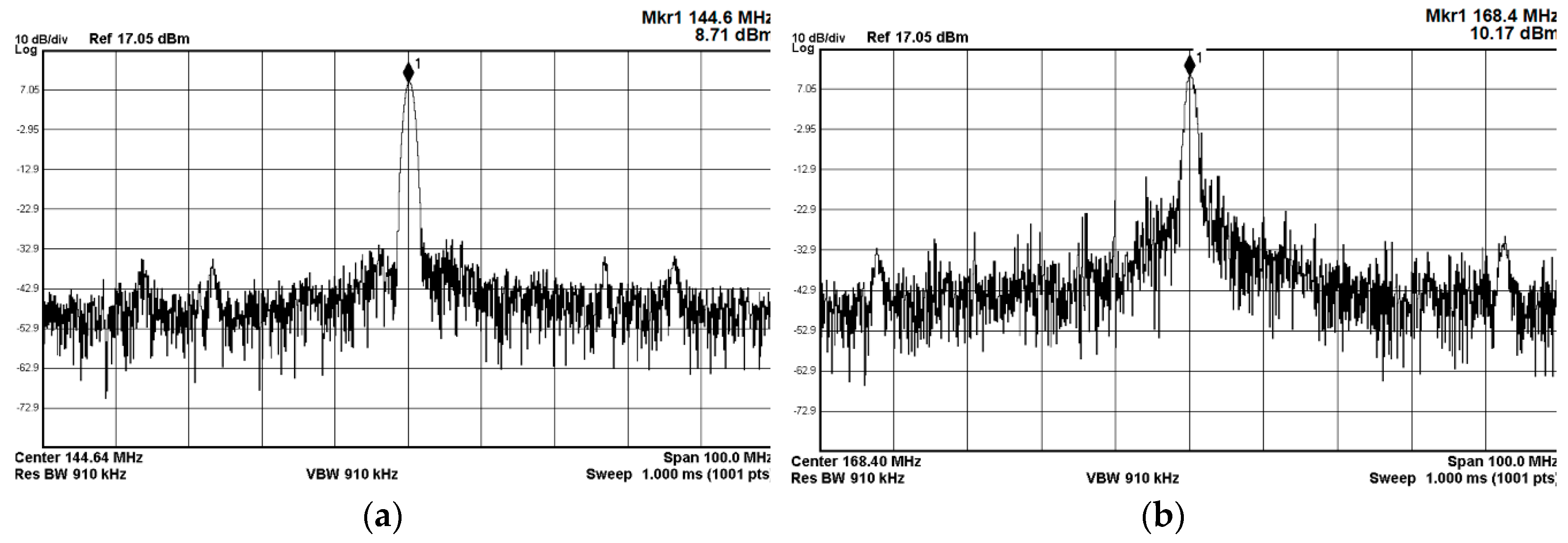
The frequency spectrum measurement results of the proposed LC DCO divided by a 64 output when operating at the lowest and highest operating frequencies are shown in Figure 7. From the latter picture (a), it is seen that the lowest output signal frequency (when dividing by 64) was 144.6 MHz. This resulted in the proposed LC DCO generating a 144.6 MHz × 64 = 9.25 GHz frequency signal. The highest output signal frequency (when dividing from 64) was 168.4 MHz, which is shown in Figure 7b. The LC DCO generated a 168.4 MHz × 64 = 10.78 GHz frequency signal.
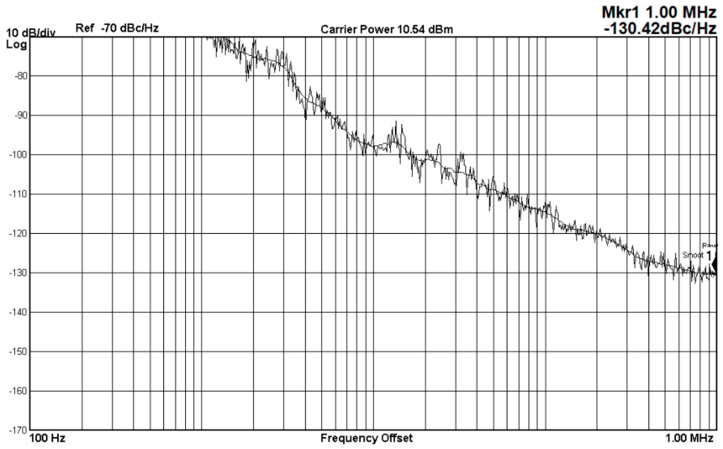
The phase noise at the designed LC DCO output (divided by 64 when operating at the lowest frequency) is shown in Figure 8. From this, it is visible that the phase noise at 1 MHz offset frequency from the DCO lowest (En bit = 0) carrier frequency was −130.42 dBc/Hz output of the frequency divider when operating at the lowest frequencies.
It was noted that the phase noise at 1 Mhz offset from frequency divider’s output frequency when the DCO was operating at the lowest frequency (En bit = 0, FMIN = 144.6 MHz) was −130.42 dBc/Hz at the divider output. The phase noise at 1 MHz offset frequency from the DCO highest carrier frequency (En bit = 63, FMAX = 168.4 GHz) was −128.13 dBc/Hz at the divider output. These parameters were obtained by measuring the phase noise at the divide-by-64 output. This theory revealed that at each divider cascade, phase noise improved by 3 dBc/Hz [11]. Therefore, it was possible to estimate the real LC DCO phase noise at the input of the first of the six divider cascades (F/64): −130.42 + (3 × 6) = −113.42 dBc/Hz at 1 MHz offset from the lowest LC DCO carrier frequency (FMIN = 9.25 GHz) and −128.51 + (3 × 6) = −110.51 dBc/Hz at 1 MHz offset from the highest LC DCO carrier frequency (FMAX = 10.78 GHz). During the post-layout simulations, the following phase noise values were obtained: −114.79 dBc/Hz at 1 MHz offset from the lowest LC DCO carrier frequency and −113.62 dBc/Hz at 1 MHz offset from the highest LC DCO carrier frequency.
Table 2 shows the proposed LC DCO performance compared with other reported LC DCOs. The table shows that all compared DCOs were designed using 65 nm technology, while this paper’s proposed LC DCO, which was designed using 130 nm technology, lead to reduced production cost of the chip. The lowest supply voltage was used in [12] and was equal to 1.1 V, which affected the lowest power consumption of the LC DCO core −3.3 mW. All of the reviewed and reported DCOs had a carrier frequency that varied around 10 GHz. The widest DCO tuning range was [13] DCO (15.12%). The lowest phase noise result was in the proposed LC DCO and reached –113.42 dBc/Hz at 1 MHz offset frequency from the lowest carrier frequency. It was possible to achieve such low phase noise due to the high quality inductor. The FOM and FOMT values of the proposed LC DCO were –183.52 dBc/Hz and –187.20 dBc/Hz, respectively. These results were achieved due to very low phase noise (–113.52 dBc/Hz) and wide frequency tuning range (15.28%).

4. Prototype Test-Bench

The layout of the proposed LC DCO with the E-TSPC frequency divider is shown in Figure 9. The total layout area with pads was 1.5 mm × 1.5 mm. The largest part of the layout in the proposed LC DCO had an area of about 193 µm × 311 µm. The largest part of the LC DCO was the inductor L—184 µm × 184 µm. The E-TSPC divider occupied a 304 µm × 44 µm area of the chip. One pad occupied 160 µm × 324 µm. Other dimensions presented in Figure 9.
The LC DCO and frequency divider IC in quad flat no-leads (QFN) with a 20 pads package is presented in Figure 10a. The manufactured chip was packed into a QFN 20 pads package. The main benefits of this package over the traditional small outline integrated circuit (SOIC), the shrink small outline package (SSOP), the thin shrink small outline package (TSSOP), or the thin very small outline package (TVSOP) are: the packages are physically smaller and allow the chips to be used on small printed circuit boards (PCBs), which reduces the cost and dimensions of the gadget; the QFN package has a smaller area of the route, which reduces the length of interconnections, resulting in reduced parasitic impedances and capacities; improved heat efficiency—in the case of high thermal conductivity, IC is better cooled; and finally, QFN packages have low inductance and capacitance and reduced electrical parasites allow for higher frequencies, which is why this package is suitable for RF solutions [16,17].
The LC DCO and E-TSPC frequency divider IC in the printed circuit test board is presented in Figure 10b. The PCB test board dimensions were 73 × 50 mm. The PCB had two layers and was 1.6 mm thick. The dielectric layer was made of FR-4, a fiberglass-reinforced epoxy-laminated material used in printed circuit board manufacturing. For PCB pads, hot air solder leveling finish (HASL) was used. The power supply pin headers were located on the right side of the PCBl. The IC control switches were placed on the top of the PCB. The E-TSPC divider input (DIV IN) and outputs (DIV32 and DIV16) were oriented on the right side and the bottom. The presented LC DCO and E-TSPC divider outputs (DCO64 and DCO 256) were oriented on the bottom and the left side. The designed LC DCO and E-TSPC divider IC (IC1) was oriented on the center of the PCB, and the output buffers (IC2 and IC5) were oriented in the bottom of the IC1. SubMiniature version A (SMA) connectors were used for high frequency outputs and inputs (J3, J4, J5, J6, J7), and these connectors had a 50 Ω impedance. SMA was designed for use from 0 Hz to 18 GHz [18].

5. Conclusions

The main goal of this work was to design a low power, low phase noise, wide tuning range, low-area, and low-cost LC DCO and frequency divider IC for ITS systems working on a 5G network. The main difficulty was getting the required parameters and performance using the 130 nm IC technology, but the main advantage of the IC technology was the cheapness of the ICs produced. The proposed LC DCO was designed for USA and Japan 5G frequency bands. The proposed LC DCO output signal frequency divided by four and sixteen could be applied to the USA 5G network (2.5 LTE B24 and 600 MHz USA 5G bands), and the output signal frequency divided by two could be applied to the 4.4–4.9 GHz Japan 5G band.
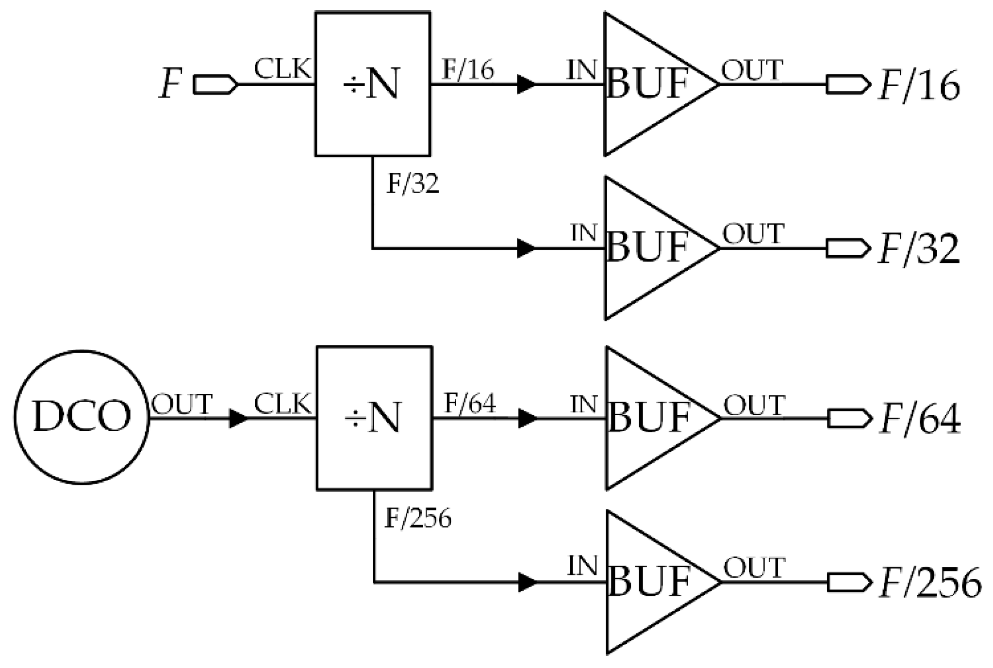
The designed IC consisted of two parts: the LC DCO frequency generation and division circuit and the divider testing circuit. The LC DCO frequency generation and division circuit in two outputs generated a LC DCO signal frequency divided by 64 and 256 times. The divider testing circuit divided the frequency of the input signal by 16 and by 32. Using the proposed high frequency E-TSPC divider, the output frequency of the LC DCO could be divided from two to 256 times.
Simulations and measurements were performed in nominal conditions using 1.8 V supply voltage and 40 °C temperature. The LC DCO achieved a wide tuning range from 10.07 GHz to 11.16 GHz when schematics were simulated. Frequency varied from 9.54 GHz to 10.56 GHz when the post-layout was simulated, and frequency varied from 9.25 GHz to 10.78 GHz when the chip was measured.
Measured phase noise at 1 MHz offset frequency from the LC DCO lowest carrier frequency was −113.42 dBc/Hz, and phase noise at 1 MHz offset frequency from the LC DCO highest carrier frequency was −110.51 dBc/Hz. During the post-layout simulations, the following phase noises were obtained: −114.79 dBc/Hz at 1 MHz offset from the lowest LC DCO carrier frequency and −113.62 dBc/Hz at 1 MHz offset from the highest LC DCO carrier frequency.
The measured average power consumption of the proposed LC DCO IC core was 10.02 mW, which was higher than it was during both the schematic and the post-layout simulations, which were equal to 8.73 mW and 9.15 mW, respectively. The measured power consumption average of the proposed E-TSPC divider IC was 97.52 mW, which was also higher than it was during both the schematic and the post-layout simulations, which were 90.05 mW and 93.21 mW, respectively. To optimize power consumption, it is possible to limit the current to optimum using the “current control” block.
The FOM and FOMT values of the proposed LC DCO were −183.52 dBc/Hz and −187.20 dBc/Hz, respectively. These results were achieved due to very low phase noise (−113.52 dBc/Hz) and wide frequency tuning range (15.28%).
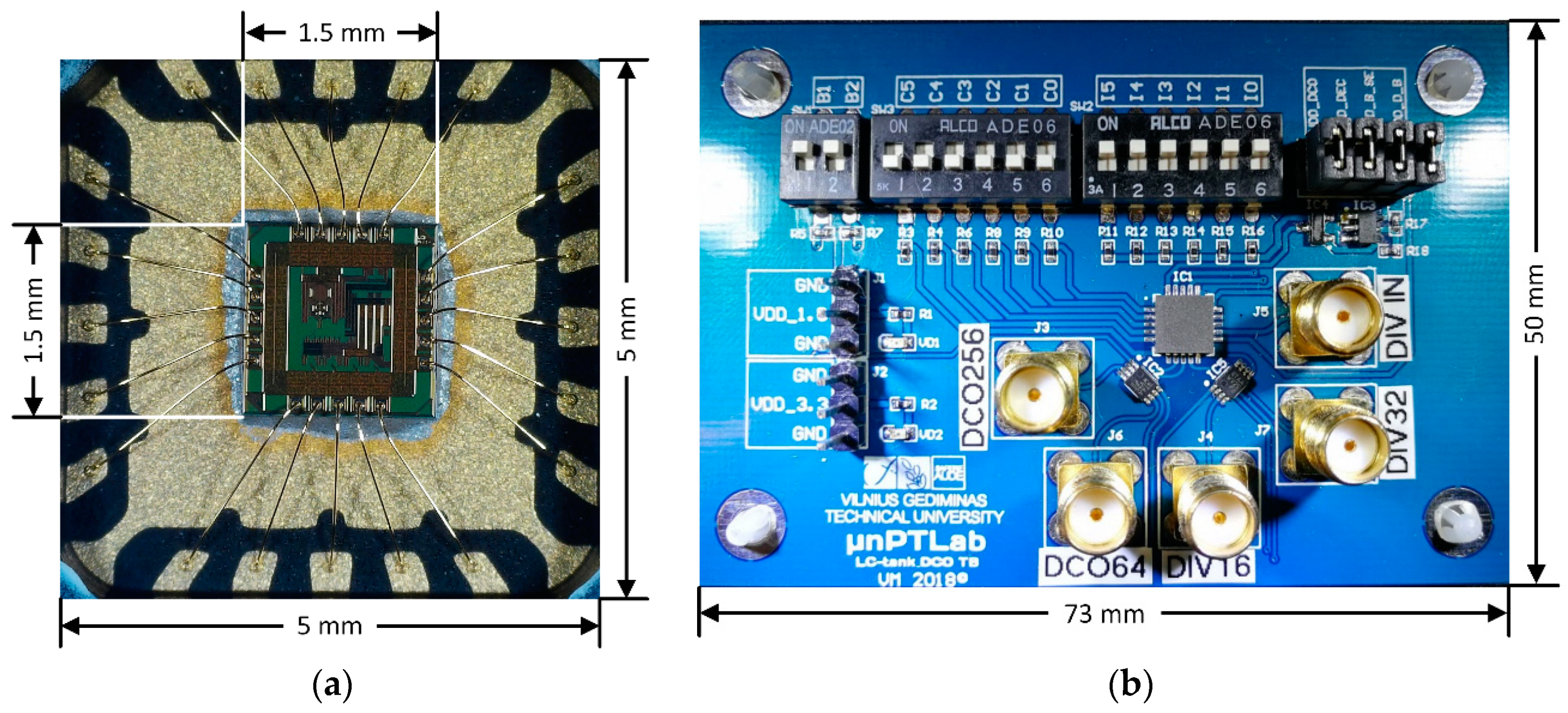
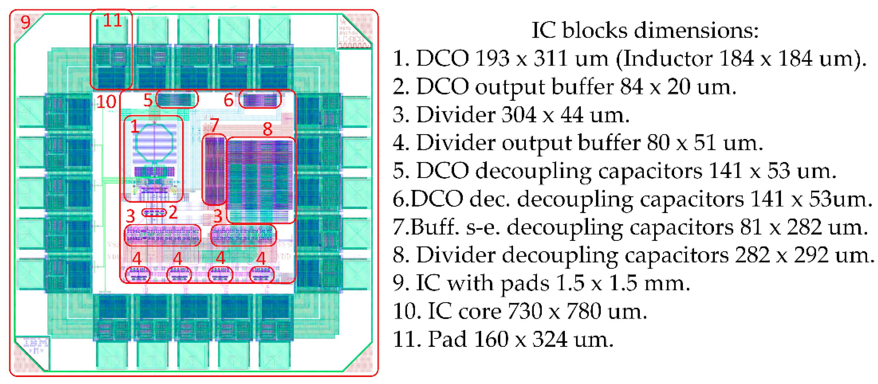
The total layout area with pads was 1.5 mm × 1.5 mm. The largest part of the layout was occupied by the proposed LC DCO, with an area of about 193 µm × 311 µm, while the largest part of the LC DCO was the inductor L—184 µm × 184 µm.

Author Contributions

All authors contributed to the present paper with the same effort in finding available literature resources, conducting both simulations and measurements, as well as writing the paper.

Funding

This research was funded by the Research Council of Lithuania grant number DOTSUT-235, No. 01.2.2-LMT-K-718-01-0054 as a part of “Design and Research of Internet of Things (IoT) Framework Model and Tools for Intelligent Transport Systems” project. The APC was funded by Vilnius Gediminas technical university Faculty of Electronics.

Acknowledgments

The authors would like to thank the project “Design and Research of Internet of Things (IoT) Framework Model and Tools for Intelligent Transport Systems” team and Vaidotas Barzdėnas for organizing prototype chip manufacturing, as well as Aleksandr Vasjanov for observations while writing this paper.

Conflicts of Interest

The authors declare no conflict of interest.

References

  1. Vasjanov, A.; Barzdenas, V. A Review of Advanced CMOS RF Power Amplifier Architecture Trends for Low Power 5G Wireless Networks. Electronics 2018, 7, 271. [Google Scholar] [CrossRef]
  2. Kashyap, K.K.P.; Patel, K. Charge Pump, Loop Filter and VCO for Phase Lock Loop Using 0.18 µm CMOS Technology. IOSR J. VLSI Signal Process. 2013, 2, 21–25. [Google Scholar] [CrossRef]
  3. Molaei, H.; Hajsadeghi, K. A low power high resolution time to digital converter for ADPLL application. In Proceedings of the 2016 IEEE 59th International Midwest Symposium on Circuits and Systems (MWSCAS), Abu Dhabi, UAE, 16–19 October 2016; pp. 1–4. [Google Scholar]
  4. Tiebout, M. Low Power VCO Design in CMOS; Springer: Berlin/Heidelberg, Germany, 2006; Volume 20. [Google Scholar]
  5. Macaitis, V.; Navickas, R. CMOS technology based LC VCO review. In Proceedings of the 2015 Open Conference of Electrical, Electronic and Information Sciences (eStream), Vilnius, Lithuania, 21 April 2015; pp. 1–4. [Google Scholar]
  6. Macaitis, V.; Navickas, R. Design of multicore digitally controlled oscillator in 65 nm CMOS technology. In Proceedings of the 2017 Open Conference of Electrical, Electronic and Information Sciences (eStream), Vilnius, Lithuania, 27 April 2017; pp. 1–4. [Google Scholar]
  7. Tzschoppe, C.; Jorges, U.; Richter, A.; Lindner, B.; Ellinger, F. Theory and design of advanced CMOS current mirrors. In Proceedings of the 2015 SBMO/IEEE MTT-S International Microwave and Optoelectronics Conference (IMOC), Porto de Galinhas, Brazil, 3–6 November 2015; pp. 1–5. [Google Scholar]
  8. Heydarzadeh, S.; Torkzadeh, P.; Pourmina, M. A 12 GHz programmable fractional-n frequency divider with 0.18um CMOS technology. In Proceedings of the 2013 5th Computer Science and Electronic Engineering Conference (CEEC), Colchester, UK, 17–18 September 2013; Volume 26, No. 6. pp. 29–33. [Google Scholar]
  9. Nemitha, B.; Pradeep Kumar, B.P. Speed Analysis of Body Biased TSPC and ETSCPC Flip Flops. Int. J. Sci. Res. 2014, 3, 847–850. [Google Scholar]
  10. Jurgo, M.; Kiela, K.; Navickas, R. Design of Low Noise 10 GHz divide by 16…511 Frequency Divider. Electron. Electr. Eng. 2013, 19, 87–90. [Google Scholar] [CrossRef]
  11. Apostolidou, M.; Baltus, P.G.M.; Vaucher, C.S. Phase noise in frequency divider circuits. In Proceedings of the 2008 IEEE International Symposium on Circuits and Systems, Seattle, WA, USA, 18–21 May 2008; pp. 2538–2541. [Google Scholar]
  12. Da Dalt, N.; Kropf, C.; Burian, M.; Hartig, T.; Eul, H. A 10b 10GHz digitlly controlled LC oscillator in 65 nm CMOS. In Proceedings of the 2006 IEEE International Solid State Circuits Conference - Digest of Technical Papers, San Francisco, CA, USA, 6–9 February 2006; Volume 51, pp. 669–678. [Google Scholar]
  13. Lou, L.; Chen, B.; Tang, K.; Zheng, Y. A CMOS digital-controlled oscillator for All-digital PLL frequency synthesizer. In Proceedings of the 2016 International Symposium on Integrated Circuits (ISIC), Singapore, 2–14 December 2016; pp. 1–4. [Google Scholar]
  14. Seller, N.; Chataigner, E.; Lapuyade, H.; Begueret, J.-B. A Distributed Voltage Controlled Oscillator in a standard 65nm CMOS Process. In Proceedings of the 2006 Ph.D. Research in Microelectronics and Electronics, Otranto, Italy, 12–15 June 2006; pp. 93–96. [Google Scholar]
  15. Seller, N.; Cathelin, A.; Lapuyade, H.; Begueret, J.-B.; Chataigner, E.; Belot, D. A 10GHz Distributed Voltage Controlled Oscillator for WLAN Application in a VLSI 65 nm CMOS Process. In Proceedings of the 2007 IEEE Radio Frequency Integrated Circuits (RFIC) Symposium, Honolulu, HI, USA, 3–5 June 2007; pp. 115–118. [Google Scholar]
  16. Mortan, F.; Wright, L. Quad Flatpack No-Lead Logic Packages. 2004. Available online: http://www.ti.com/lit/an/scba017d/scba017d. pdf (accessed on 8 October 2018).
  17. Xi, J.; Xiao, F.; Wang, H. Comparative study on the reliability of QFN and AAQFN packages. In Proceedings of the 2014 15th International Conference on Electronic Packaging Technology, Chengdu, China, 12–15 August 2014; Volume 96, pp. 959–9620. [Google Scholar]
  18. Frequency Range Chart for RF Connectors_Amphenol RF. Available online: https://www.amphenolrf.com/frequency-range-chart/ (accessed on 4 October 2018).
Figure 1. Basic block diagrams of: (a) conventional phase locked loop (CPLL) synthesizer; (b) all digital phase locked loop (ADPLL) synthesizer.
Electronics 08 00072 g001
Figure 2. Simplified architecture of N-channel metal oxide semiconductor (NMOS) LC digitally controlled oscillator (LC DCO) cores: (a) current source (CS) connected to ground (VSS); (b) CS connected to supply (VDD). Simplified architecture of P-channel metal oxide semiconductor (PMOS) LC DCO cores: (c) CS connected to VSS; (d) CS connected to VDD.
Electronics 08 00072 g002aElectronics 08 00072 g002b
Figure 3. Simplified block diagram of the proposed LC DCO and frequency divider. DCO—digitally controlled oscillator, ÷N—frequency divider, BUF—output buffer, F—frequency divider input signal, F/N—frequency divider signal frequency divided by coefficient N.
Electronics 08 00072 g003
Figure 4. Schematic of the proposed LC DCO.
Electronics 08 00072 g004
Figure 5. Extended true single phase clock (E-TSPC) frequency divider: (a) divide by two stage schematic; (b) block diagram.
Electronics 08 00072 g005
Figure 6. Tuning range of the proposed LC DCO.
Electronics 08 00072 g006
Figure 7. Frequency spectrum measurement results of the proposed LC DCO divide-by-64 output (a) when operating at the lowest operating frequency, and (b) when operating at highest operating frequency. Measurements were performed using Keysight Technologies N9010A EXA signal analyzer.
Electronics 08 00072 g007
Figure 8. Phase noise measurement results of the proposed DCO divide-by-64 output when operating at the lowest operating frequency (144.6 MHz). Measurements were performed using Keysight Technologies N9010A EXA signal analyzer.
Electronics 08 00072 g008
Figure 9. Layout of the proposed LC DCO and E-TSPC frequency divider with pads and dimensions.
Electronics 08 00072 g009
Figure 10. LC DCO and frequency divider IC: (a) in quad flat no-leads (QFN) with 20 pads package, and (b) in printed circuit test board (PCB).
Electronics 08 00072 g010
Table 1. Main parameters of the proposed LC DCO and E-TSPC divider.
ParameterSchematicLayoutMeasurements
VDD, V1.81.81.8
Technology, nm130
FMIN, GHz10.79.549.25
FMAX, GHz11.610.5610.78
F0, GHz11.1510.0510.01
F, GHz; %0.9; 8.71.02; 10.151.53; 15.28
PN@1 MHz, dBc/Hz−116.21−114.79−113.42
PDCO, mW8.739.1510.02
PDIV, mW90.593.2197.52
FOM, dBc/Hz−187.74−185.22−183.52
FOMT, dBc/Hz−185.88−185.35−187.20
VDD—supply voltage; technology—integrated circuit (IC) technology; FMIN—lowest LC DCO output signal frequency; FMAX—highest LC DCO output signal frequency; F0—central LC DCO output signal frequency; ∆F—LC DCO frequency tuning range; PN@1MHz—LC DCO phase noise at 1 MHz offset frequency at lowest LC DCO carrier frequency; PDCO—LC DCO power consumption; PDIV—E-TSPC divider power consumption; FOM—figure of merit; FOMT—figure of merit including the tuning range.
Table 2. Performance of the proposed LC DCO compared with other LC DCOs.
Parameter[12][13][14][15]This Work **
VDD, V1.11.21.221.8
Technology, nm65656565130
FMIN, GHz9.8713.699.6010.609.25
FMAX, GHz10.9215.9311.6011.7010.78
F0, GHz10.4014.8110.6011.1510.01
F, %10.1015.129.879,8715.28
PN@1 MHz, dBc/Hz−102.00−99.00−101.00−116.00−113.42
P, mW3.3019.8029.0036.0010.02
FOM, dBc/Hz−177.15−169.44−166.88–181.38−183.52
FOMT, dBc/Hz−177.24−173.04−172.40−181.26−187.20
** Parameters of IC measurement.

