Resonant Converter with Voltage-Doubler Rectifier or Full-Bridge Rectifier for Wide-Output Voltage and High-Power Applications


Abstract
:1. Introduction
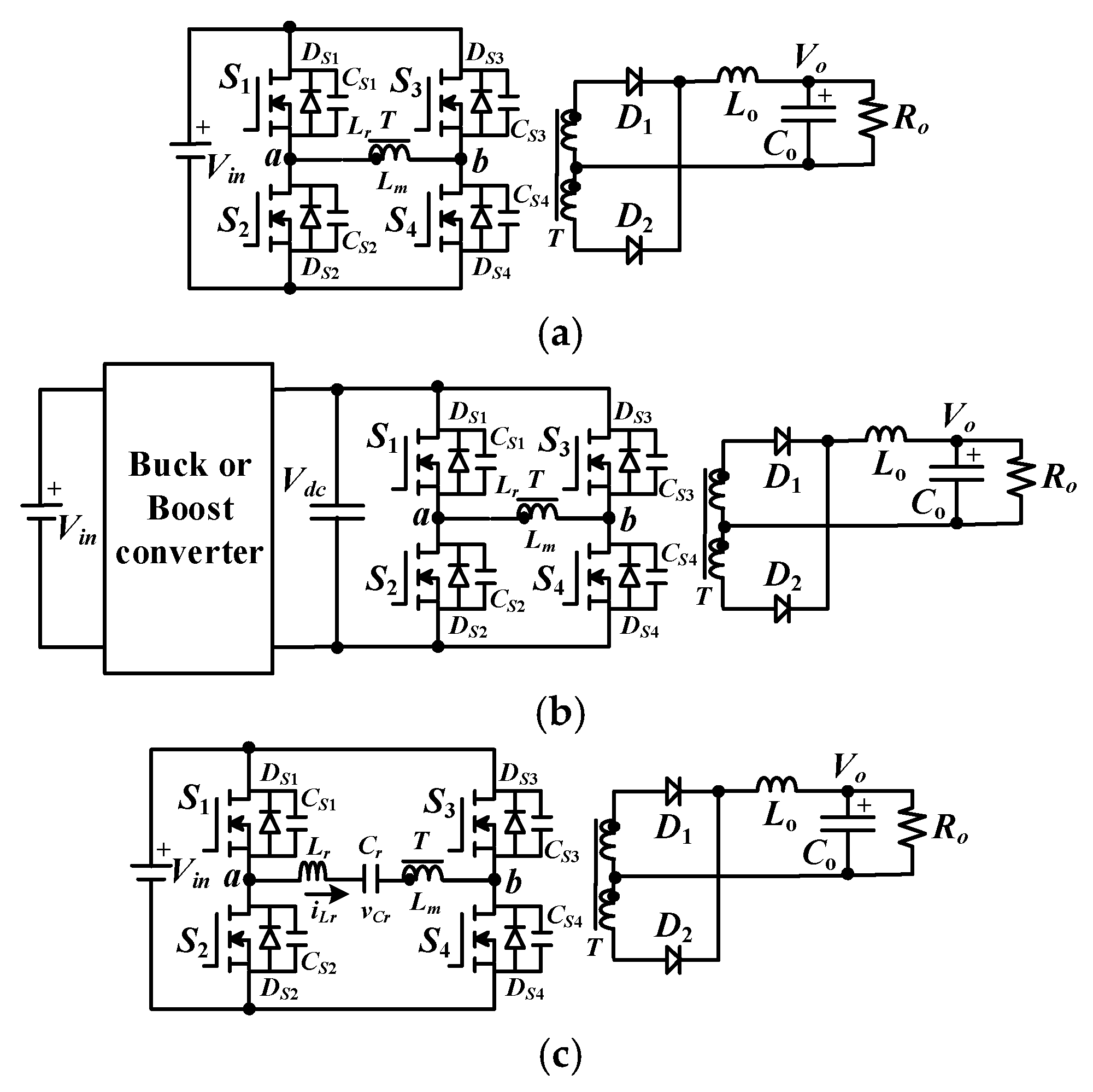
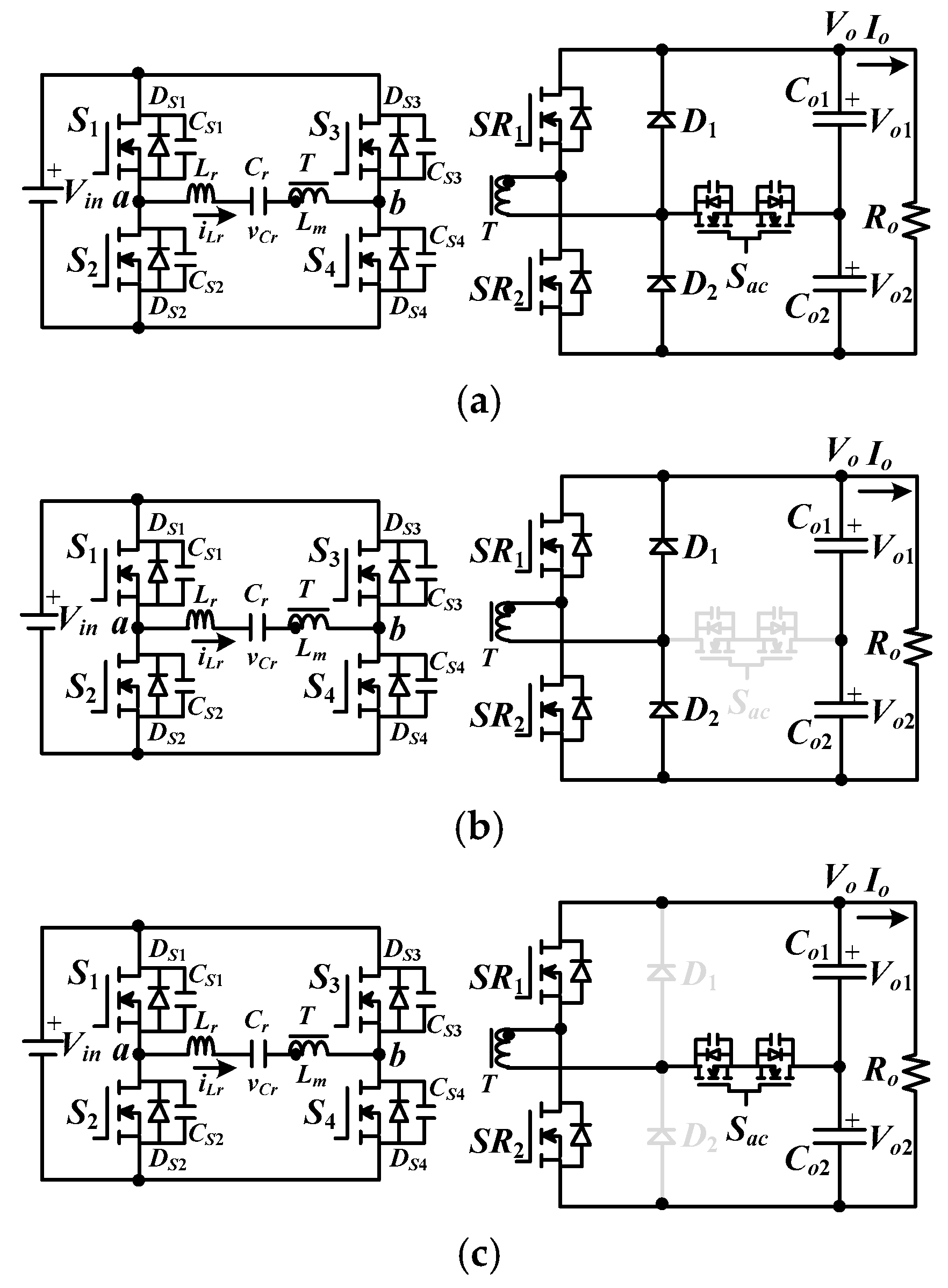
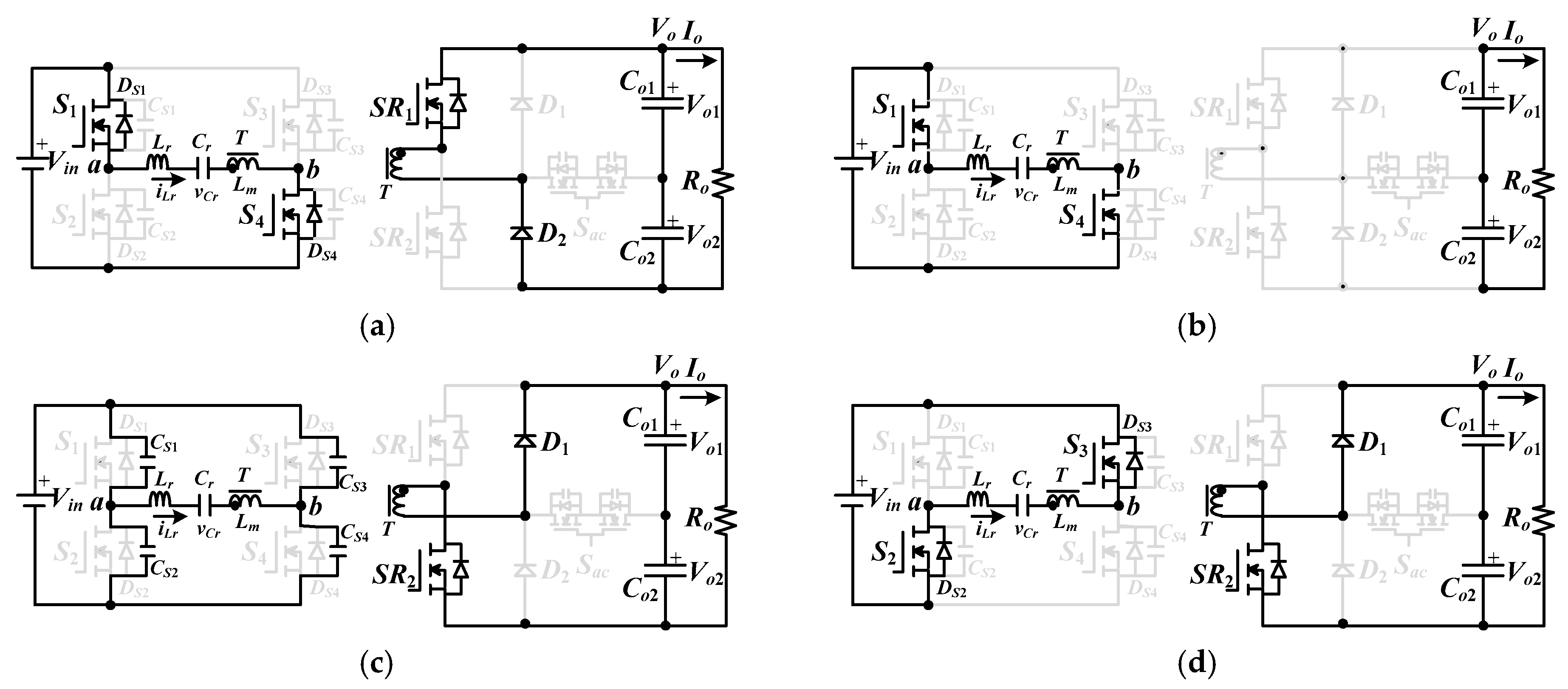
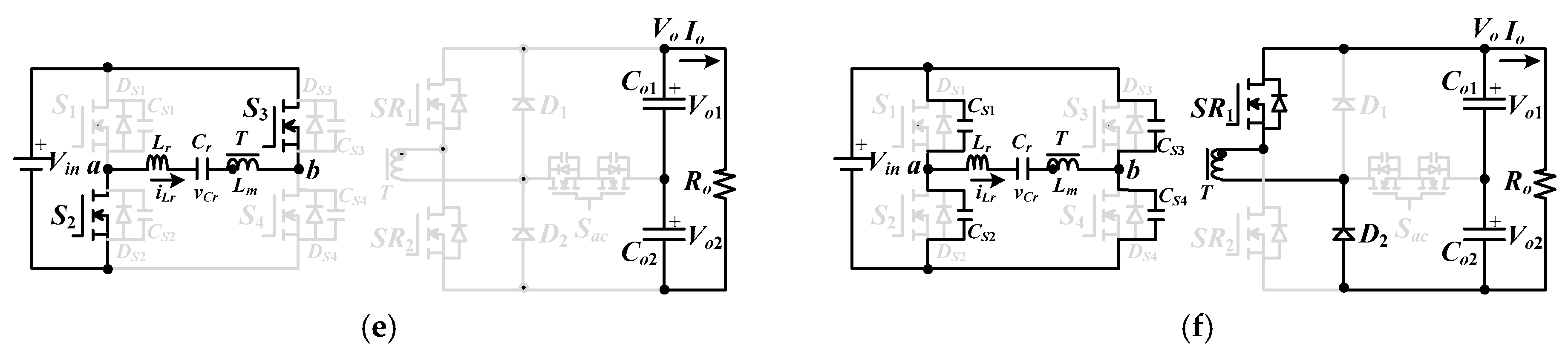
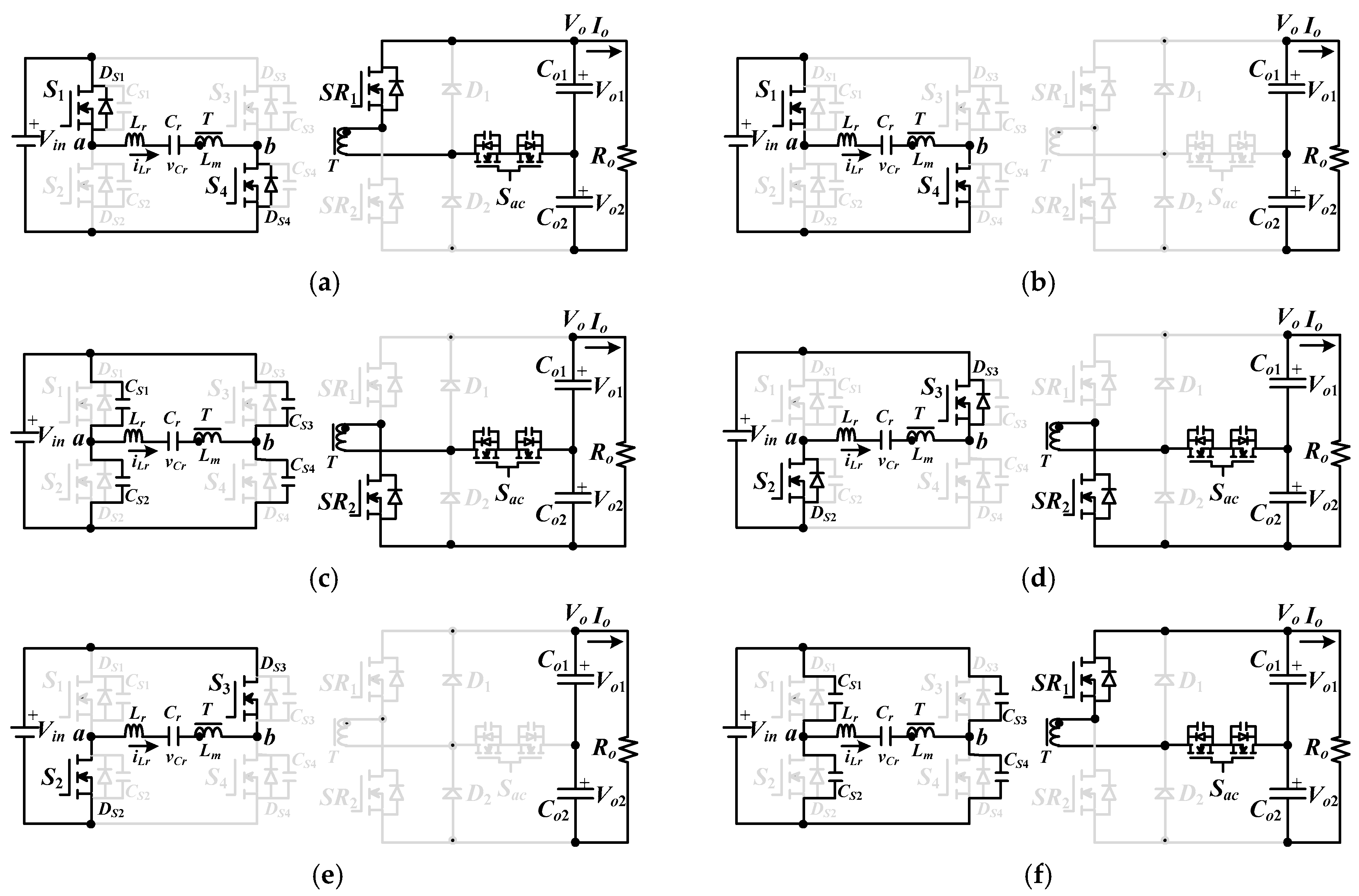
2. Circuit Diagram
3. Operation Principle of the Proposed Converter
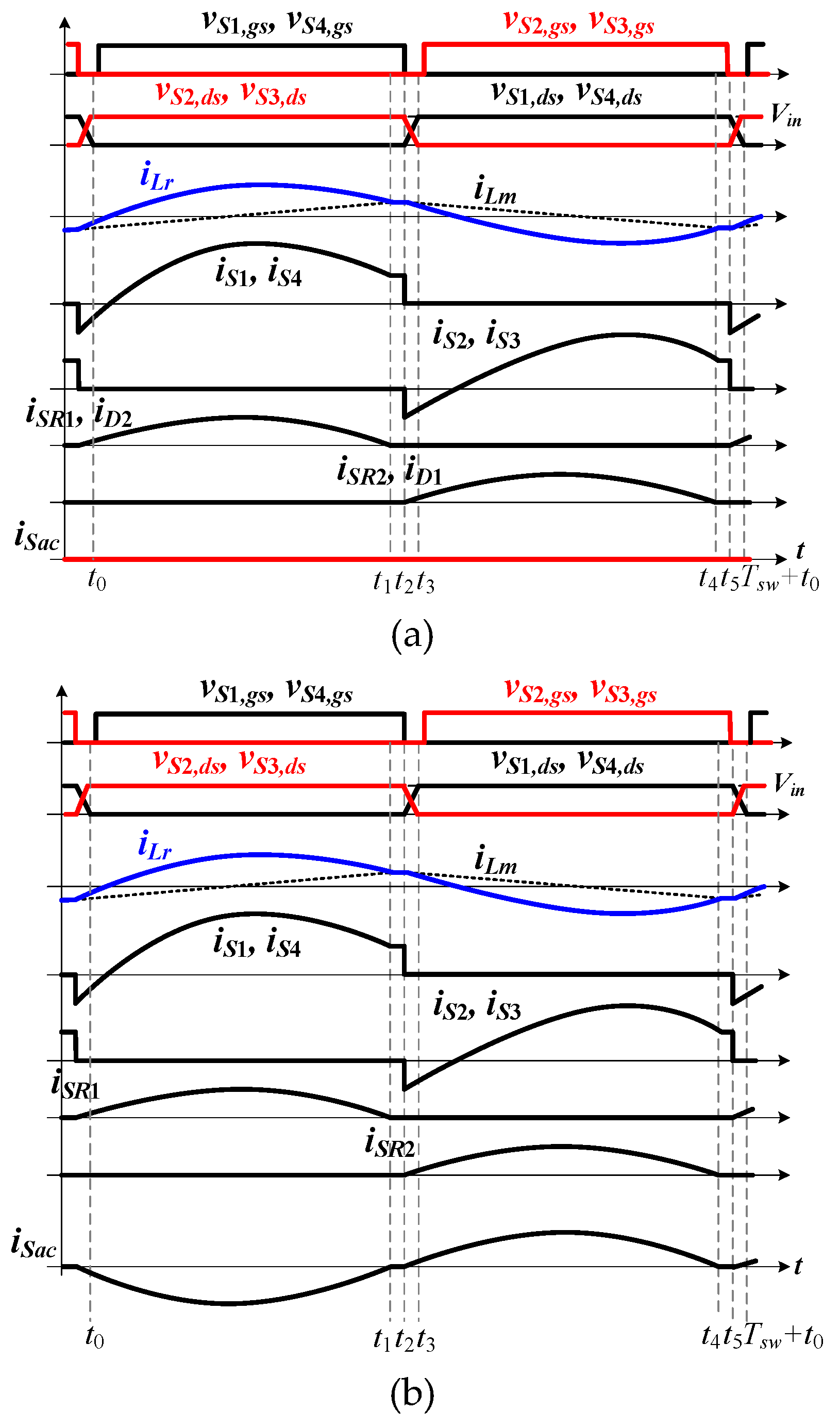
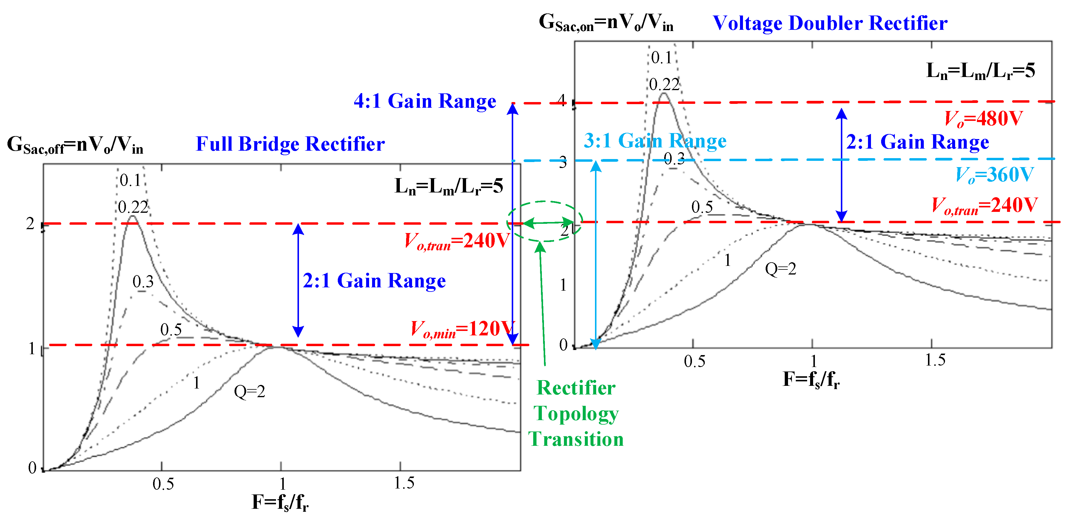
3.1. For Low Output Voltage with Sac Off (Full-Bridge Rectifier)
3.2. For High Output Voltage with Sac on (Voltage Double Rectifier)
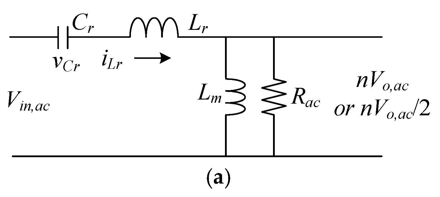
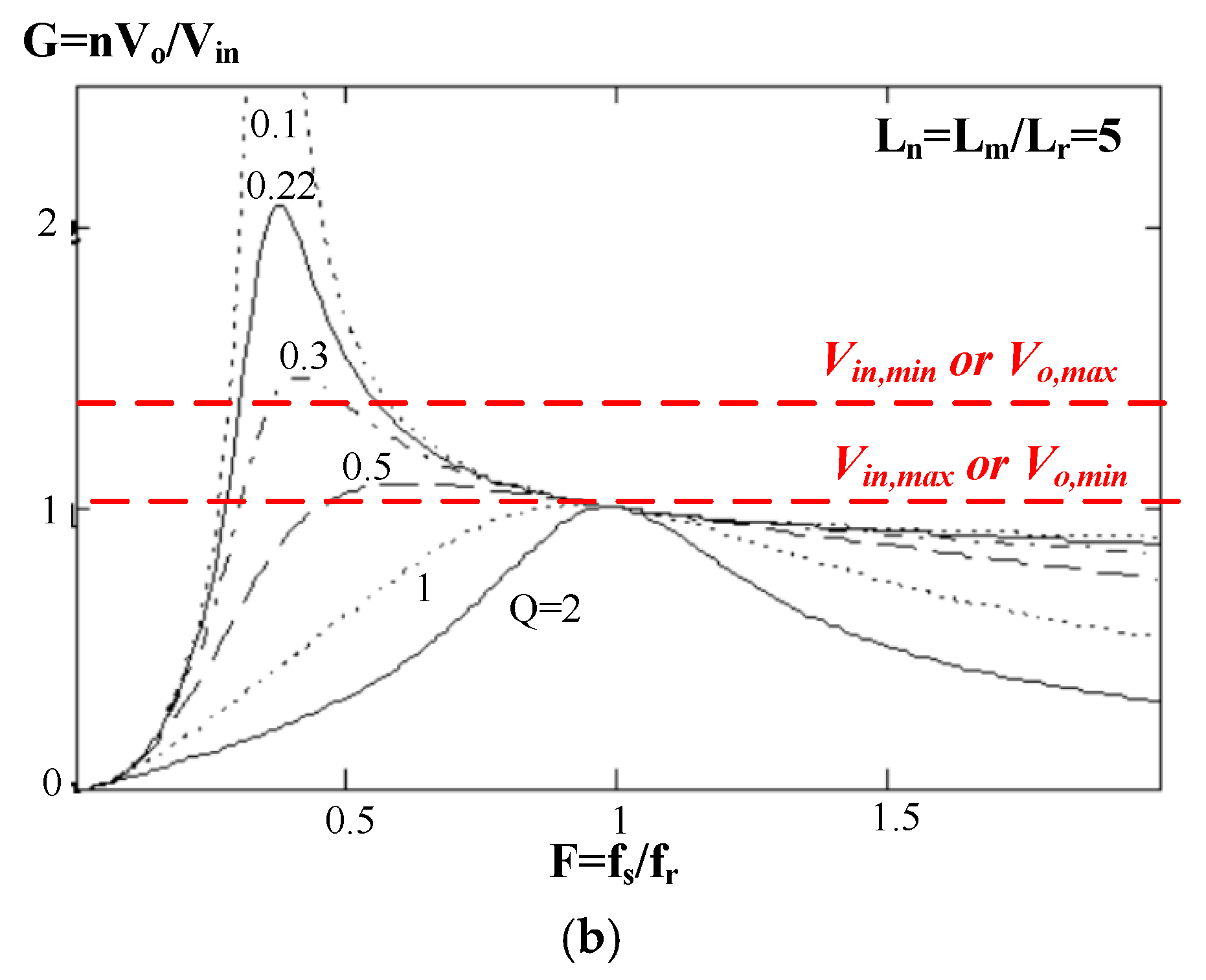
4. Circuit Characteristics and Design Considerations
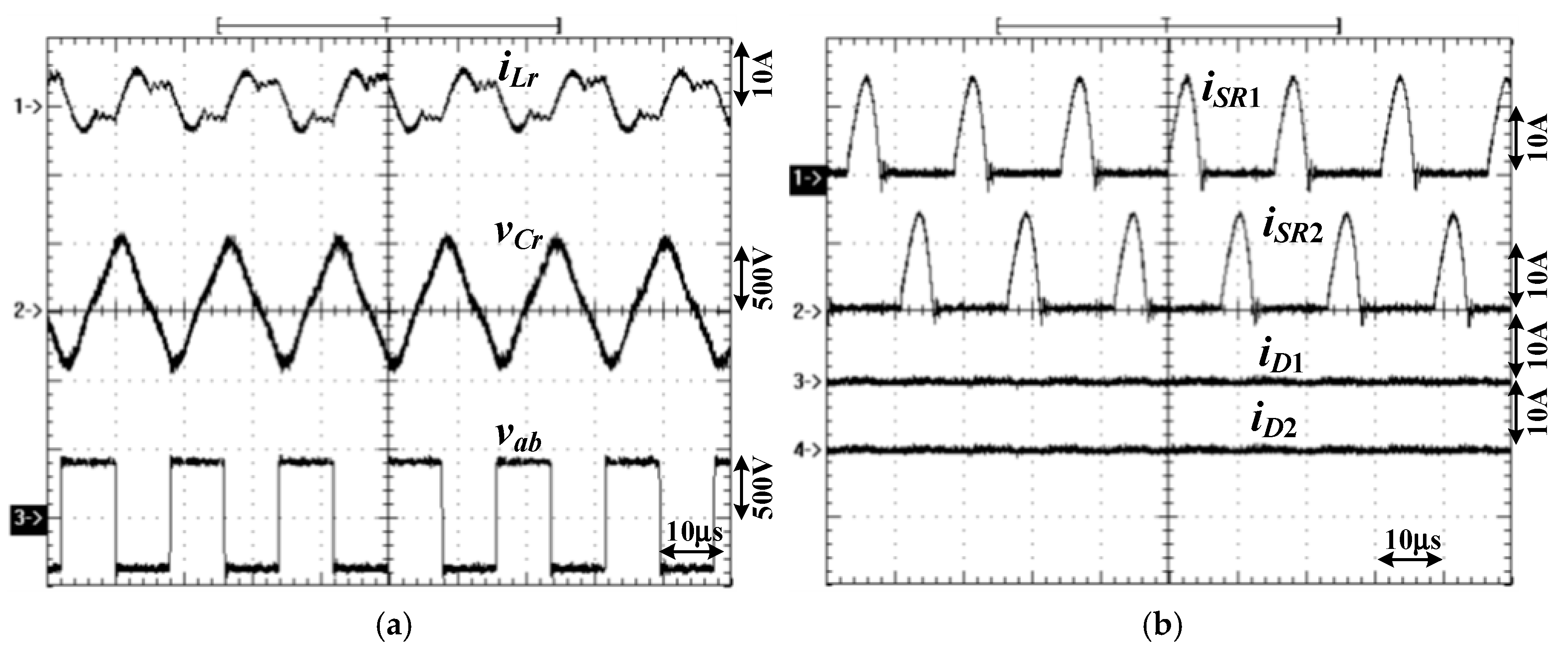
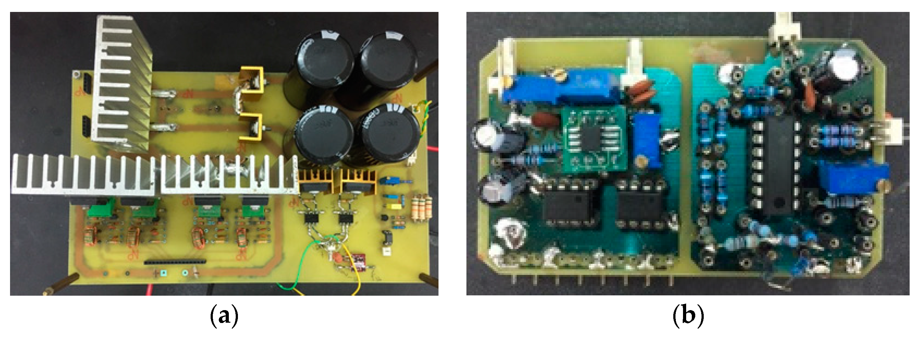
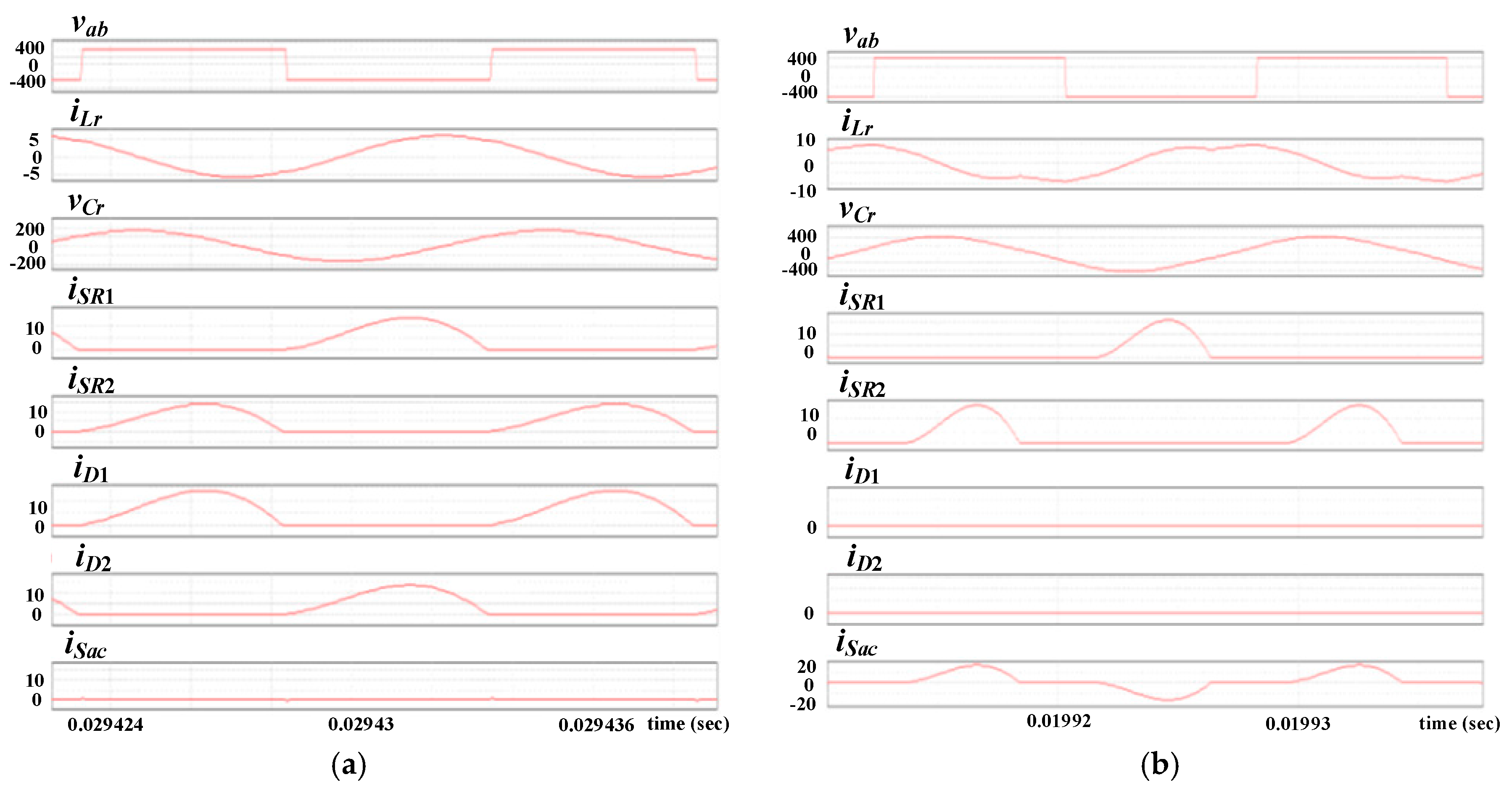
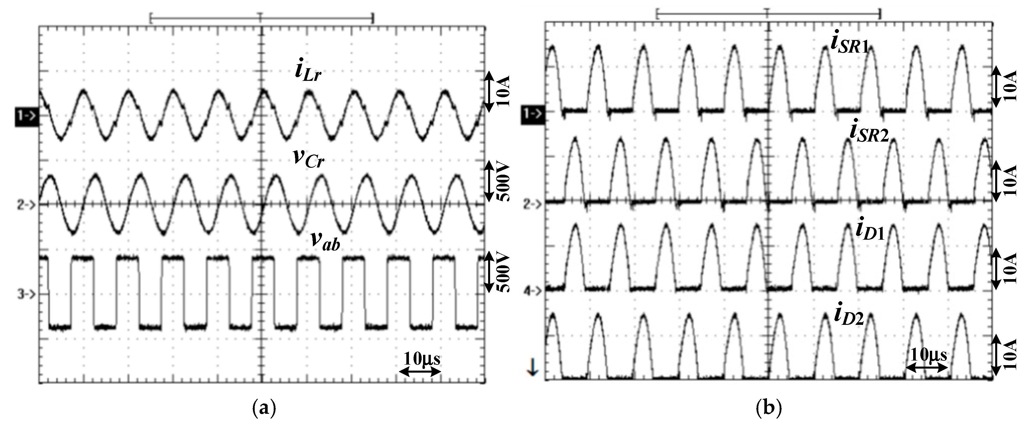
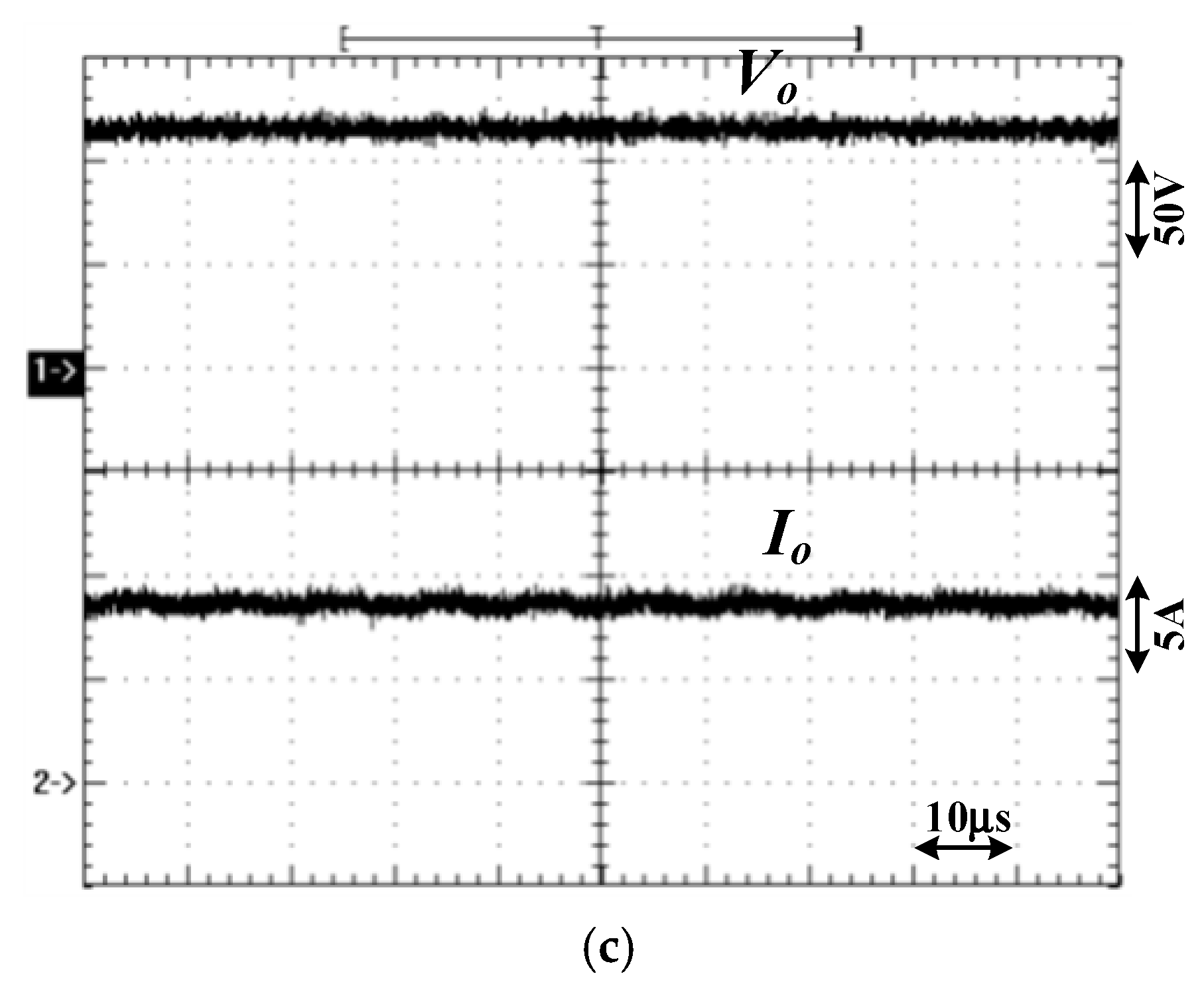
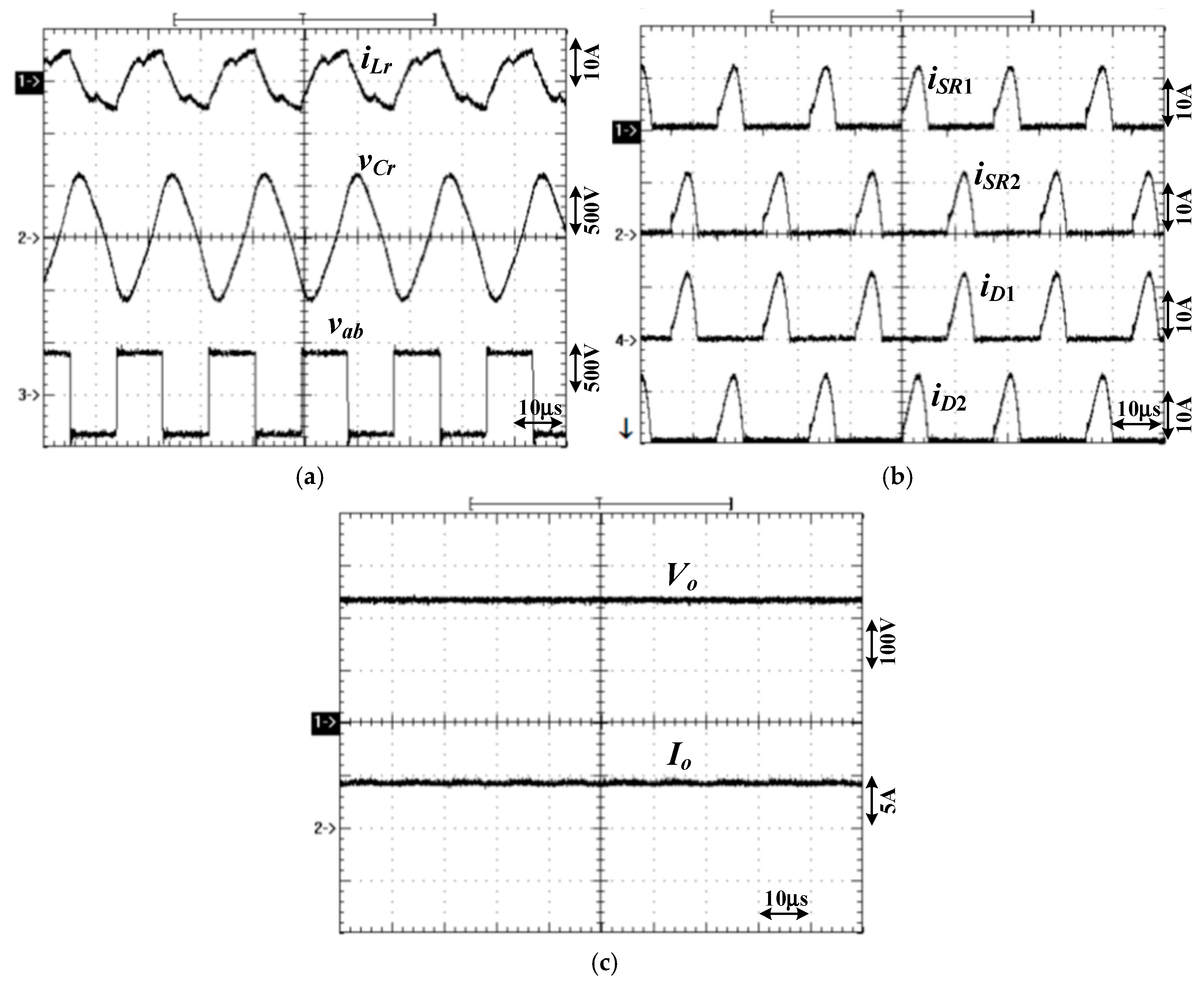
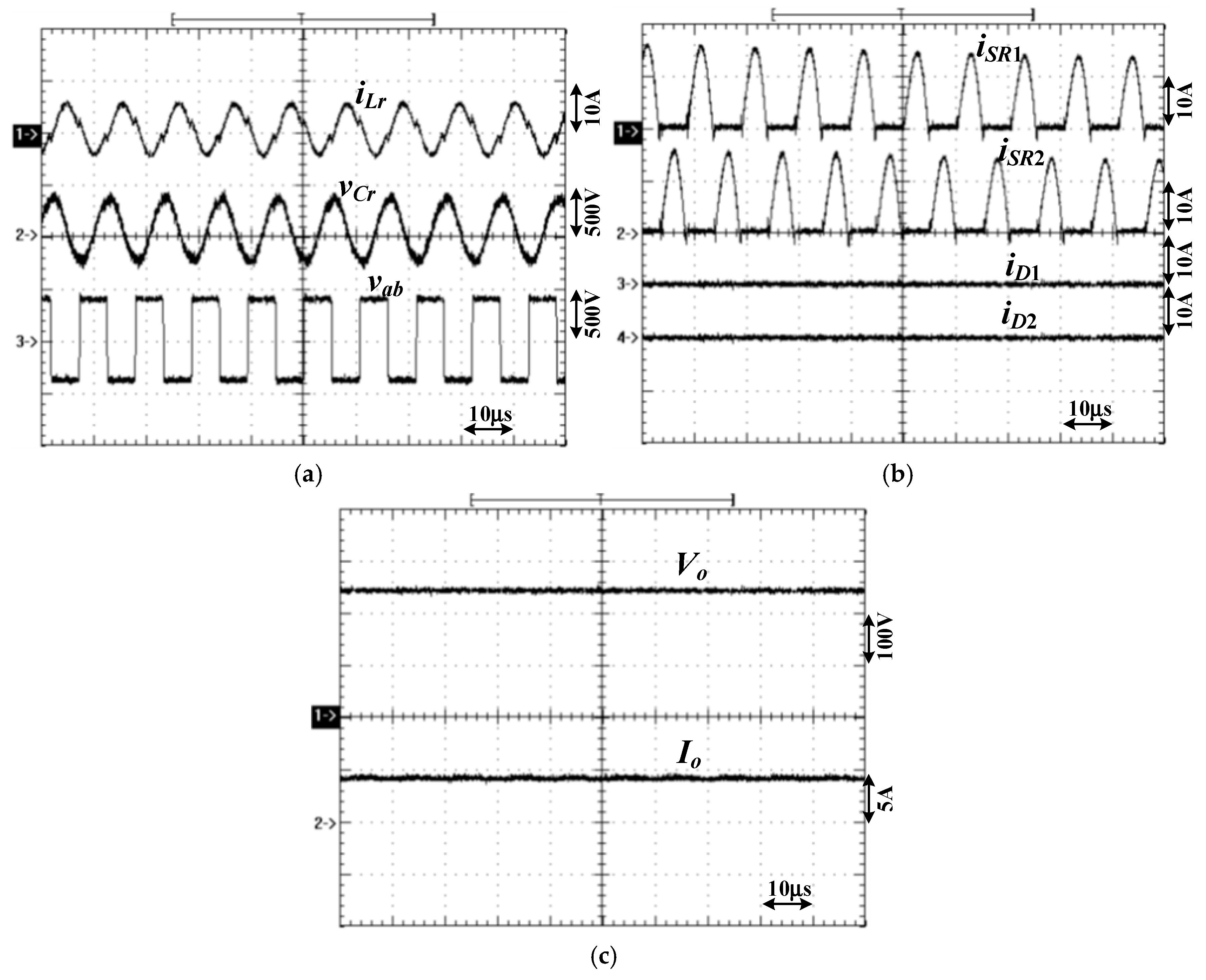
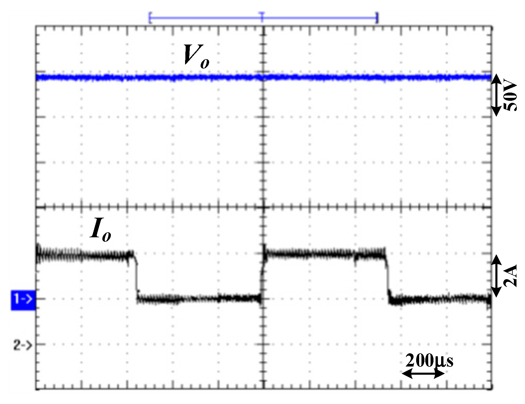
5. Experimental Results
6. Conclusions
Author Contributions
Funding
Conflicts of Interest
References
- Kim, J.-W.; Han, J.-K.; Lai, J.-S. APWM adapted half-bridge LLC converter with voltage doubler rectifier for improving light load efficiency. Electron. Lett. 2017, 53, 339–341. [Google Scholar] [CrossRef]
- Kanamarlapudi, V.R.K.; Wang, B.; So, L.P.; Wang, Z. Analysis, design, and implementation of an APWM ZVZCS full-bridge DC–DC converter for battery charging in electric vehicles. IEEE Trans. Power Electron. 2017, 32, 6145–6160. [Google Scholar] [CrossRef]
- Ali, K.; Das, P.; Panda, S.K. Analysis and design of APWM half-bridge series resonant converter with magnetizing current assisted ZVS. IEEE Trans. Ind. Electron. 2017, 64, 1993–2003. [Google Scholar] [CrossRef]
- Lin, B.R.; Chao, C.H. A new ZVS DC/DC converter with three APWM circuits. IEEE Trans. Ind. Electron. 2013, 60, 4351–4358. [Google Scholar] [CrossRef]
- Liu, P.J.; Hsu, Y.C.; Hsu, S.R. Drain-voltage balance and phase-shifted PWM control schemes for high-efficiency parallel-string dimmable LED drivers. IEEE Trans. Ind. Electron. 2018, 65, 6168–6176. [Google Scholar] [CrossRef]
- Lee, I.O.; Moon, G.W. Phase-shifted PWM converter with a wide ZVS range and reduced circulating current. IEEE Trans. Power Electron. 2013, 28, 908–919. [Google Scholar] [CrossRef]
- Safaee, A.; Jain, P.; Bakhshai, A. A ZVS pulsewidth modulation full-bridge converter with a low-RMS-current resonant auxiliary circuit. IEEE Trans. Power Electron. 2016, 31, 4031–4047. [Google Scholar] [CrossRef]
- Pahlevani, M.; Pan, S.; Jain, P. A hybrid phase-shift modulation technique for DC/DC converters with a wide range of operating conditions. IEEE Trans. Ind. Electron. 2016, 63, 7498–7510. [Google Scholar] [CrossRef]
- Li, Z.; Wu, T.; Zhang, G.; Yang, R. High modulation method combining variable frequency and double phase-shift for a 10 kW LLC resonant converter. IET Power Electron. 2018, 11, 2161–2169. [Google Scholar] [CrossRef]
- Singh, A.K.; Das, P.; Panda, S.K. Analysis and design of SQR-based high-voltage LLC resonant dc-dc converter. IEEE Trans. Power Electron. 2017, 32, 4466–4481. [Google Scholar] [CrossRef]
- Haga, H.; Kurokawa, F. Modulation method of a full-bridge three-level LLC resonant converter for battery charger of electric vehicles. IEEE Trans. Power Electron. 2017, 32, 2498–2507. [Google Scholar] [CrossRef]
- Zhang, C.; Gao, Z.; Liao, X. Bidirectional dc-dc converter with series-connected resonant tanks to realize soft switching. IET Power Electron. 2018, 11, 2029–2043. [Google Scholar] [CrossRef]
- Sun, W.; Xing, Y.; Wu, H.; Ding, J. Modified high-efficiency LLC converters with two split resonant branches for wide input-voltage range applications. IEEE Trans. Power Electron. 2018, 33, 7867–7870. [Google Scholar] [CrossRef]
- Jovanović, M.M.; Irving, B.T. On the fly topology-morphing control efficiency optimization method for LLC resonant converters operating in wide input and/or output-voltage range. IEEE Trans. Power Electron. 2016, 31, 2596–2608. [Google Scholar] [CrossRef]


© 2018 by the authors. Licensee MDPI, Basel, Switzerland. This article is an open access article distributed under the terms and conditions of the Creative Commons Attribution (CC BY) license (http://creativecommons.org/licenses/by/4.0/).
Share and Cite
Lin, B.-R.; Lin, G.-H.; Jian, A. Resonant Converter with Voltage-Doubler Rectifier or Full-Bridge Rectifier for Wide-Output Voltage and High-Power Applications. Electronics 2019, 8, 3. https://doi.org/10.3390/electronics8010003
Lin B-R, Lin G-H, Jian A. Resonant Converter with Voltage-Doubler Rectifier or Full-Bridge Rectifier for Wide-Output Voltage and High-Power Applications. Electronics. 2019; 8(1):3. https://doi.org/10.3390/electronics8010003
Chicago/Turabian StyleLin, Bor-Ren, Guan-Hong Lin, and Aries Jian. 2019. "Resonant Converter with Voltage-Doubler Rectifier or Full-Bridge Rectifier for Wide-Output Voltage and High-Power Applications" Electronics 8, no. 1: 3. https://doi.org/10.3390/electronics8010003
APA StyleLin, B.-R., Lin, G.-H., & Jian, A. (2019). Resonant Converter with Voltage-Doubler Rectifier or Full-Bridge Rectifier for Wide-Output Voltage and High-Power Applications. Electronics, 8(1), 3. https://doi.org/10.3390/electronics8010003