A Radiation-Hardened Instrumentation Amplifier for Sensor Readout Integrated Circuits in Nuclear Fusion Applications


Abstract
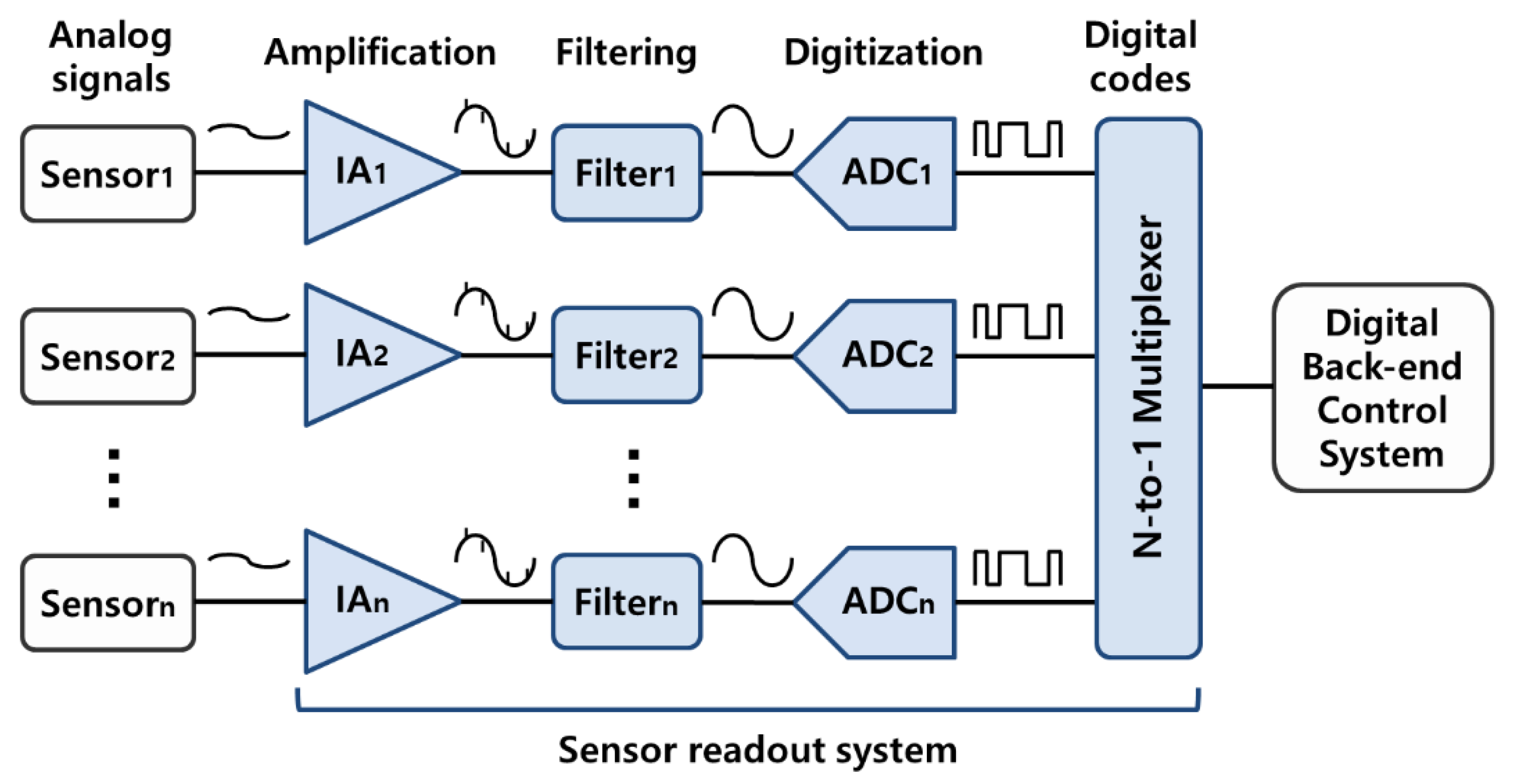
:1. Introduction
2. Radiation-Hardened IA Design
2.1. IA Topology Comparison
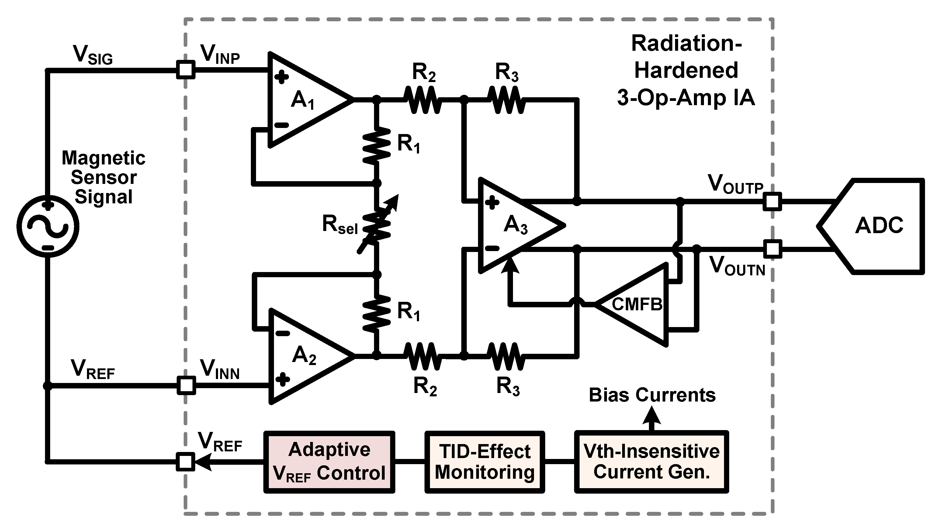
2.2. Radiation-Hardened IA Structure
3. Circuit Details for Radiation-Hardened IA
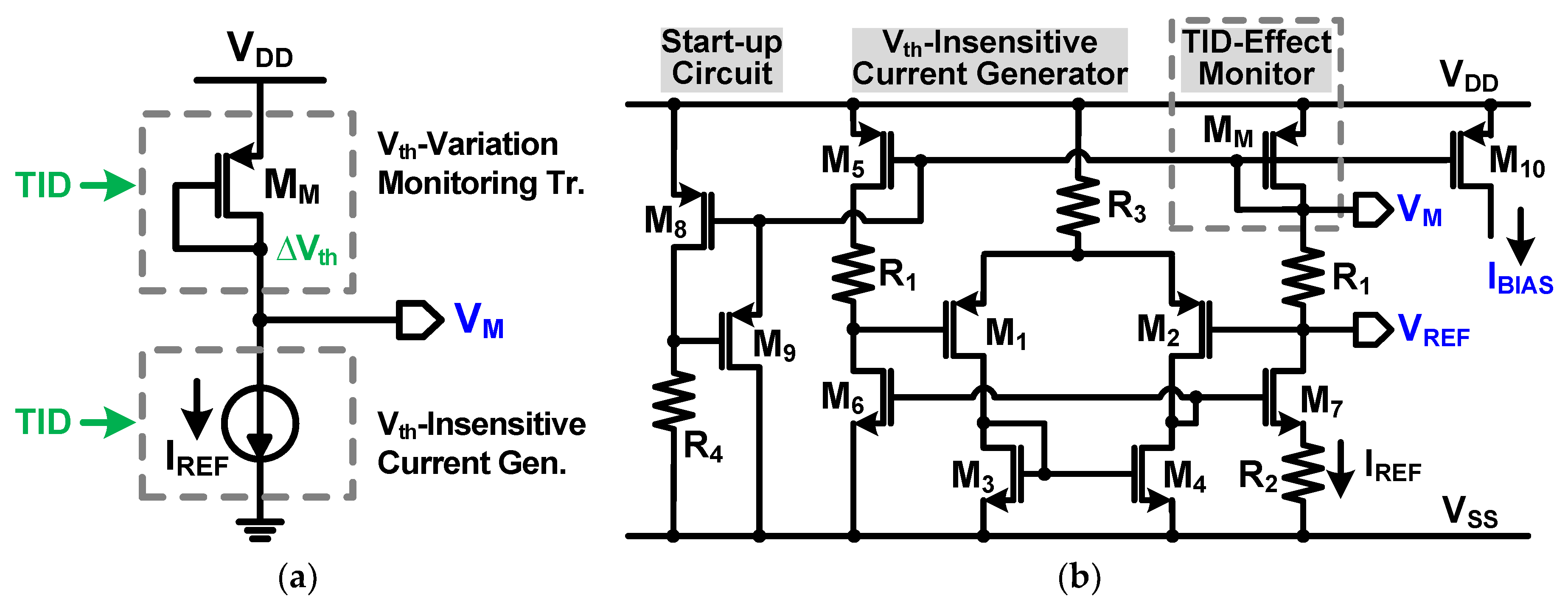
3.1. TID Effect Monitoring
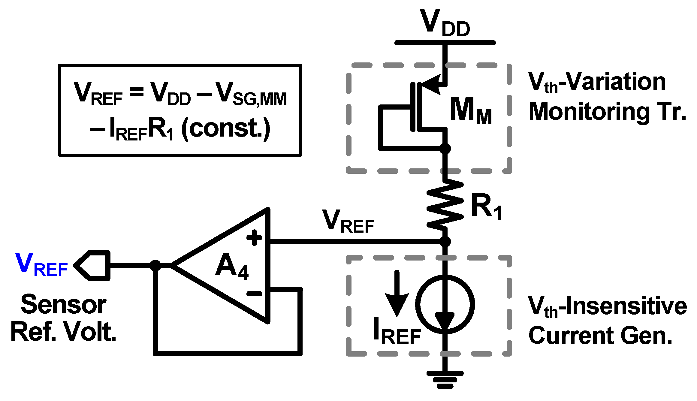
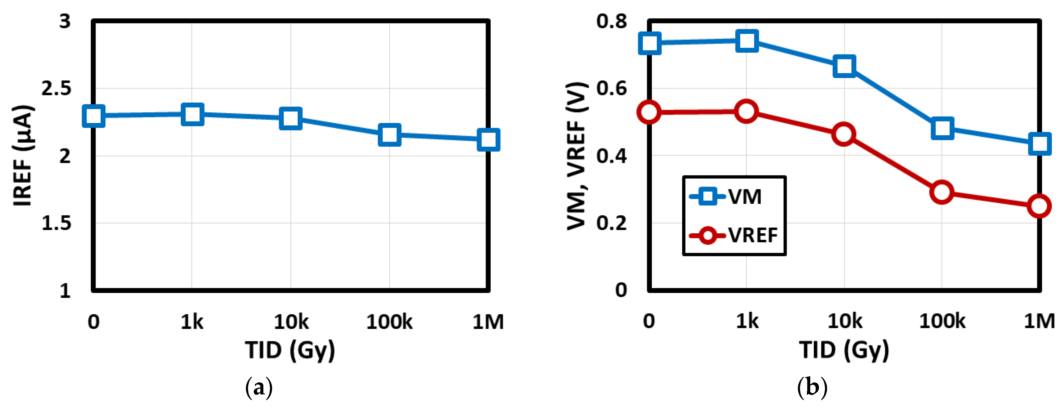
3.2. Adaptive Reference Control
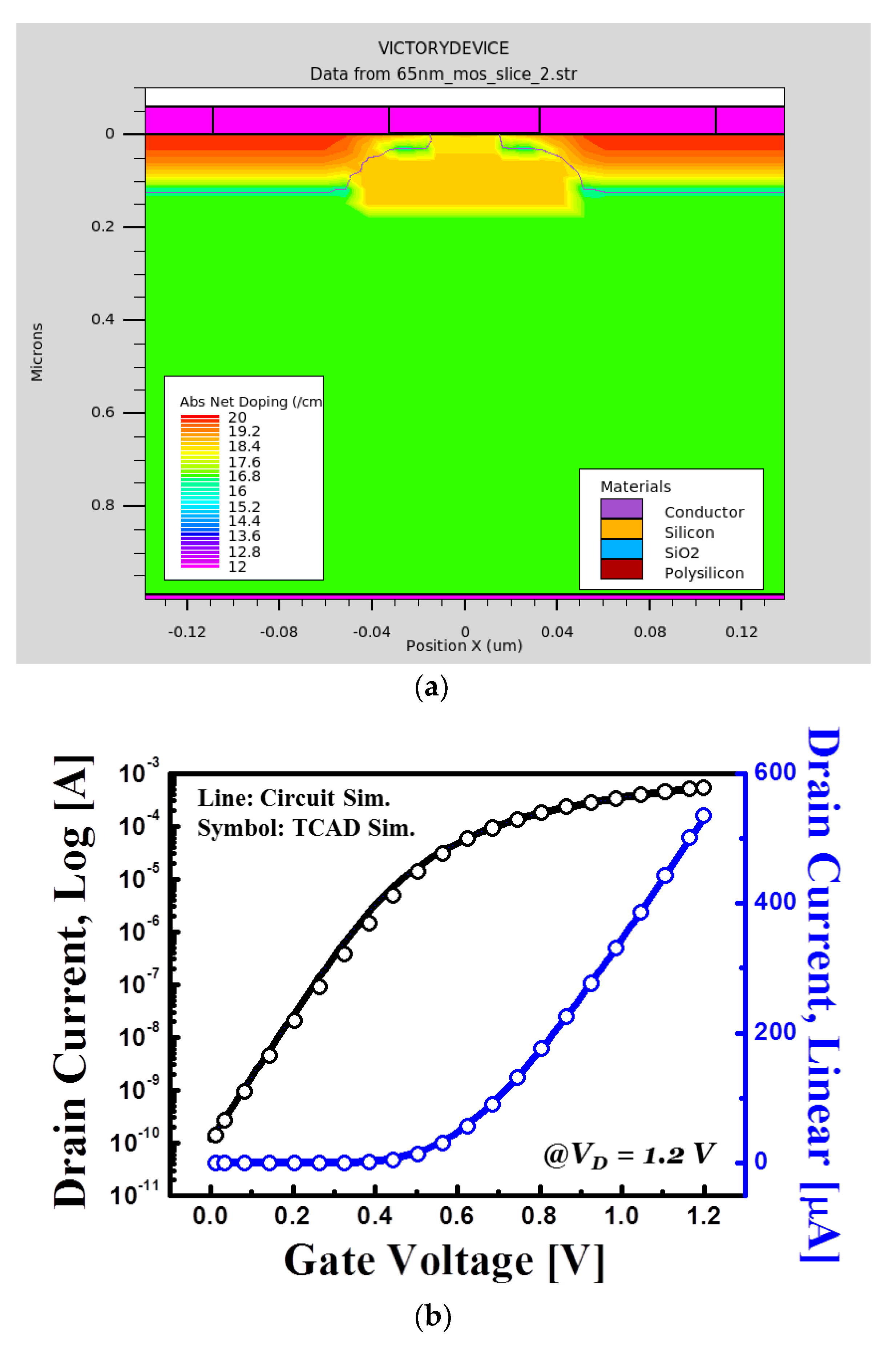
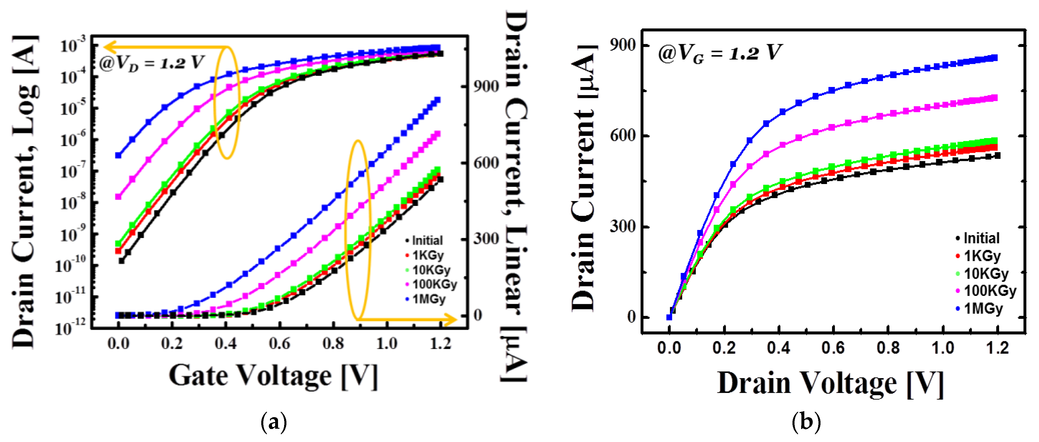
4. Compact Transistor Modeling with Radiation Effects
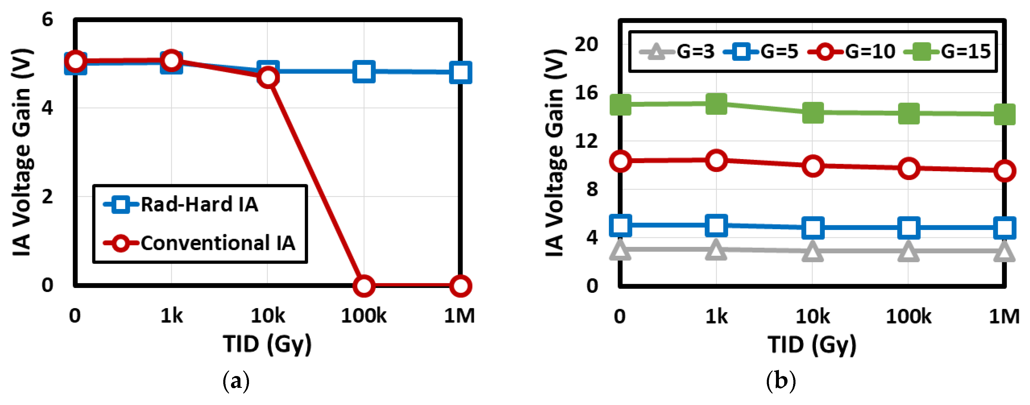
5. Simulation Results with Compact Transistor Models
6. Conclusions
Author Contributions
Funding
Acknowledgments
Conflicts of Interest
References
- Martin, V.; Bertalot, L.; Drevon, J.M.; Reichle, R.; Simrock, S.; Vayakis, G.; Walsh, M.; Verbeeck, J.; Cao, Y.; Van Uffelen, M. Electronic components exposed to nuclear radiation in ITER diagnostic systems: Current investigations and perspectives. In Proceedings of the EPS Conference on Plasma Diagnostics (ECPD), Frascati, Italy, 14–17 April 2015; pp. 1–7. [Google Scholar]
- Leroux, P.; Van Koeckhoven, W.; Verbeeck, J.; Van Uffelen, M.; Esqué, S.; Ranz, R.; Damiani, C.; Hamilton, D. Design of a MGy radiation tolerant resolver-to-digital convertor IC for remotely operated maintenance in harsh environments. Fusion Eng. Des. 2014, 89, 2314–2319. [Google Scholar] [CrossRef]
- Verbeeck, J.; Cao, Y.; Van Uffelen, M.; Casellas, L.M.; Damiani, C.; Morales, E.R.; Santana, R.R.; Meek, R.; Hais, B.; Hamilton, D.; et al. Qualification method for a 1 MGy-tolerant front-end chip designed in 65 nm CMOS for the read-out of remotely operated sensors and actuators during maintenance in ITER. Fusion Eng. Des. 2015, 96–97, 1002–1005. [Google Scholar] [CrossRef]
- Haddad, N.F.; Kelly, A.T.; Lawrence, R.K.; Li, B.; Rodgers, J.C.; Ross, J.F.; Warren, K.M.; Weller, R.A.; Mendenhall, M.H.; Reed, R.A. Incremental enhancement of SEU hardened 90 nm CMOS memory cell. IEEE Trans. Nucl. Sci. 2011, 58, 975–980. [Google Scholar] [CrossRef]
- Clark, L.T.; Mohr, K.C.; Holbert, K.E.; Yao, X.; Knudsen, J.; Shah, H. Optimizing radiation hard by design SRAM cells. IEEE Trans. Nucl. Sci. 2007, 54, 2028–2036. [Google Scholar] [CrossRef]
- Gatti, U.; Calligaro, C.; Pikhay, E.; Roizin, Y. Radiation-hardened techniques for CMOS flash ADC. In Proceedings of the IEEE International Conference on Electronics Circuits and Systems (ICECS), Marseille, France, 7–10 December 2014. [Google Scholar]
- Gromov, V.; Annema, A.J.; Kluit, R.; Visschers, J.L. A radiation hard bandgap reference circuit in a standard 0.13 μm CMOS technology. IEEE Trans. Nucl. Sci. 2007, 54, 2727–2733. [Google Scholar] [CrossRef]
- Dang, L.D.T.; Kim, J.S.; Chang, I.J. We-Quatro: Radiaiton-hardened SRAM cell with parametric process variation tolerance. IEEE Trans. Nucl. Sci. 2017, 64, 2489–2496. [Google Scholar] [CrossRef]
- Galib, M.M.H.; Chang, I.J.; Kim, J.S. Supply voltage decision methodology to minimize SRAM standby power under radiation environment. IEEE Trans. Nucl. Sci. 2015, 62, 1349–1356. [Google Scholar] [CrossRef]
- Dang, L.D.T.; Kang, M.; Kim, J.S.; Chang, I.J. Studying the variation effects of radiation hardened Quatro SRAM bit-cell. IEEE Trans. Nucl. Sci. 2016, 63, 2399–2401. [Google Scholar] [CrossRef]
- Verbeeck, J.; Van Uffelen, M.; Steyaert, M.; Leroux, P. 17 bit 4.35 mW 1 kHz delta sigma ADC and 256-to-1 multiplexer for remote handling instrumentation equipment. Fusion Eng. Des. 2013, 88, 1942–1946. [Google Scholar] [CrossRef]
- Cao, Y.; Cock, W.D.; Steyaert, M.; Leroux, P. A 4.5 MGy TID-tolerant CMOS bandgap reference circuit using a dynamic base leakage compensation technique. IEEE Trans. Nucl. Sci. 2013, 60, 2819–2824. [Google Scholar] [CrossRef]
- Virmontois, C.; Goiffon, V.; Magnan, P.; Girard, S.; Inguimbert, C.; Petit, S.; Rolland, G.; Saint-Pé, O. Displacement damage effects due to neutron and proton irradiations on CMOS image sensors manufactured in deep submicron technology. IEEE Trans. Nucl. Sci. 2010, 57, 3101–3108. [Google Scholar] [CrossRef]
- Barnaby, H.J. Total-ionizing-dose effects in modern CMOS technologies. IEEE Trans. Nucl. Sci. 2006, 53, 3103–3121. [Google Scholar] [CrossRef]
- Martin, H.; Martin-Holgado, P.; Morilla, Y.; Entrena, L.; San-Millan, E. Total ionizing dose effects on a delay-based physical unclonable function implemented in FPGAs. Electronics 2018, 7, 163. [Google Scholar] [CrossRef]
- Wu, R.; Huijsing, J.H.; Makinwa, K.A.A. Precision Instrumentation Amplifiers and Read-out Integrated Circuits; Springer: New York, NY, USA, 2013. [Google Scholar]
- Xi, X.; Dunga, M.; He, J.; Liu, W.; Cao, K.M.; Jin, X.; Ou, J.J.; Chan, M.; Niknejad, A.M.; Hu, C. BSIM4.3.0 MOSFET Model, User’s Manual; Department of Electrical Engineering and Computer Sciences, University of California: Berkeley, CA, USA, 2003. [Google Scholar]
- Jeong, Y.J.; Jeon, J.; Lee, S.; Kang, M.; Jhon, H.; Song, H.J.; Park, C.E.; An, T.K. Development of organic semiconductors based on quinacridone derivatives for organic field-effect transistors: High-voltage logic circuit applications. IEEE J. Electron Devices Soc. 2017, 5, 209–213. [Google Scholar] [CrossRef]
- Kang, M.; Lee, K.; Chae, D.H.; Park, B.-G.; Shin, H. The compact modeling of channel potential in sub-30-nm NAND flash cell string. IEEE Electron Device Lett. 2012, 33, 321–323. [Google Scholar] [CrossRef]
- Kang, M.; Park, I.H.; Chang, I.J.; Lee, K.; Seo, S.; Park, B.-G.; Shin, H. An accurate compact model considering direct-channel interference of adjacent cells in sub-30-nm NAND flash technologies. IEEE Electron Device Lett. 2012, 33, 1114–1116. [Google Scholar] [CrossRef]


| Radiation Effects | Cause | Effects to Analog Circuits |
|---|---|---|
| Total ionizing dose (TID) |
|
|
| Single event effect (SEE) |
|
|
| Displacement damage (DD) |
|
|
| IA Topologies | Capacitive-Feedback IA | Current-Feedback IA | Three-op-amp IA |
|---|---|---|---|
| TID tolerance | O (Gain ∝ capacitor ratio) | X (Gain ∝ CMOS Gm ratio) | O (Gain ∝ resistor ratio) |
| SEE tolerance | X (Capacitor voltage changes) | O (DC bias on feedback) | O (DC bias on feedback) |
| Specification | TID = 0 Gy | TID = 1 MGy |
|---|---|---|
| Process | 65-nm standard CMOS | |
| Supply voltage (V) | 1.2 | |
| Voltage gain (V/V) * | 5.008 | 4.812 |
| Bandwidth (kHz) ** | 240 | 80 |
| Power consumption (μW) ** | 34.6 | 98.3 |
| Input referred noise (μV/√Hz) ** | 0.94 | 1.12 |
| Power supply rejection ratio (dB) *** | 81 | 77.7 |
© 2018 by the authors. Licensee MDPI, Basel, Switzerland. This article is an open access article distributed under the terms and conditions of the Creative Commons Attribution (CC BY) license (http://creativecommons.org/licenses/by/4.0/).
Share and Cite
Jeong, K.; Ro, D.; Lee, G.; Kang, M.; Lee, H.-M. A Radiation-Hardened Instrumentation Amplifier for Sensor Readout Integrated Circuits in Nuclear Fusion Applications. Electronics 2018, 7, 429. https://doi.org/10.3390/electronics7120429
Jeong K, Ro D, Lee G, Kang M, Lee H-M. A Radiation-Hardened Instrumentation Amplifier for Sensor Readout Integrated Circuits in Nuclear Fusion Applications. Electronics. 2018; 7(12):429. https://doi.org/10.3390/electronics7120429
Chicago/Turabian StyleJeong, Kyungsoo, Duckhoon Ro, Gwanho Lee, Myounggon Kang, and Hyung-Min Lee. 2018. "A Radiation-Hardened Instrumentation Amplifier for Sensor Readout Integrated Circuits in Nuclear Fusion Applications" Electronics 7, no. 12: 429. https://doi.org/10.3390/electronics7120429
APA StyleJeong, K., Ro, D., Lee, G., Kang, M., & Lee, H.-M. (2018). A Radiation-Hardened Instrumentation Amplifier for Sensor Readout Integrated Circuits in Nuclear Fusion Applications. Electronics, 7(12), 429. https://doi.org/10.3390/electronics7120429