1. Introduction
Image processing has an important role in space applications enhancing the images captured by spacecrafts and robotic vehicles [
1]. However, space radiation can affect electronic devices and image sensors causing different malfunctions in the image processing system. These malfunctions can be produced by energetic particles that collide with vulnerable parts in the device leading to, for example, single event upsets (SEUs), a type of soft error that changes the value of a flip-flop or memory cell [
2].
The effects of the soft errors depend, amongst other things, on the device that is implementing the image processing algorithm. Microprocessors, for example, are widely used in the image processing field, so soft errors in some critical parts of the processor such as the program counter register can cause unexpected crashes or hangs [
3]. Likewise, field-programmable gate arrays (FPGAs) are also used to accelerate image processing algorithms since their logic blocks can be configured to exploit parallelism or specific data features [
4]. Depending on the technology used to manufacture the FPGA, they can be more or less susceptible to the mentioned radiation effects. In particular, SRAM-based FPGAs consist of two-dimensional arrays of logic cells and programmable blocks that can be configured by loading a bitstream into the SRAM cells of their configuration memory. Consequently, if an energetic particle strikes an SRAM cell, the loaded design functionalities can change permanently until the device is partial or completely reconfigured [
5].
Certain image processing operations based on local filters such as median or rank filters, need to process the image locally instead of pixel by pixel, so the entire image has to be stored in memory for further pixel reading/writing operations. As an alternative, some particular pixel caching pipelines composed of registers and first-in first-out (FIFO) line buffers can be used to process the pixel stream as it arrives from the camera. These line-buffer-based pipelines allow the local filter to process several image rows in parallel. However, local filters and pixel caching designs implemented in SRAM-based FPGAs may have malfunctions due to the mentioned configuration memory errors [
6], so an error detection or correction technique is required depending on the criticality of the application.
In this paper, a novel method to protect line-buffer-based image processing pipelines against SRAM-based FPGA configuration memory errors is presented. The technique uses two additional 8-bit registers to store pixels temporarily for later output comparisons. There are other techniques used to protect pipelines or shift registers based on modular redundancy [
7], cyclic redundancy check (CRC) [
8], or duplication and encoding [
9], but an XOR-signature scheme has been chosen for comparison with our proposed scheme due to its overhead-detection tradeoff, and its similar store-and-compare procedure with the proposed technique [
10]. The proposed and the XOR-based techniques have been compared in terms of FPGA resource usage and error detection capabilities through exhaustive fault-injection campaigns. Experimental results show that the error detection capabilities of the proposed technique are similar to the XOR-based technique, but our design uses considerably less FPGA resources. In addition to this, the proposed technique is designed in a manner that the identification of the damaged part of the pipeline can be easily inferred, so once the error is detected, a partial reconfiguration can be performed to remove the error.
The rest of the paper is organized as follows. In
Section 2, a brief introduction to local filtering and pixel caching is presented.
Section 3 explains the proposed error detection techniques for line-buffer-based image processing pipelines. These techniques are evaluated in
Section 4. Finally,
Section 5 concludes the paper.
2. Pixel Caching
In digital images, local filters are defined as operations in which the output pixel value is a function of the pixel values within a window centred on the currently analyzed input pixel [
11,
12]. In
Figure 1, the local filtering procedure is illustrated for a 3 × 3 square window.
As mentioned before, the two-dimensional window is applied to an image region and replaces its original center pixel value with the resulting filtered value of the pixels contained within the window. In order to generate the output filtered image, the window must be moved along the entire image to process each input pixel. In FPGAs, moving the window along the image means storing the whole image frame in memory for subsequent pixel readings. However, the sliding window procedure can also be achieved using a
N-by-
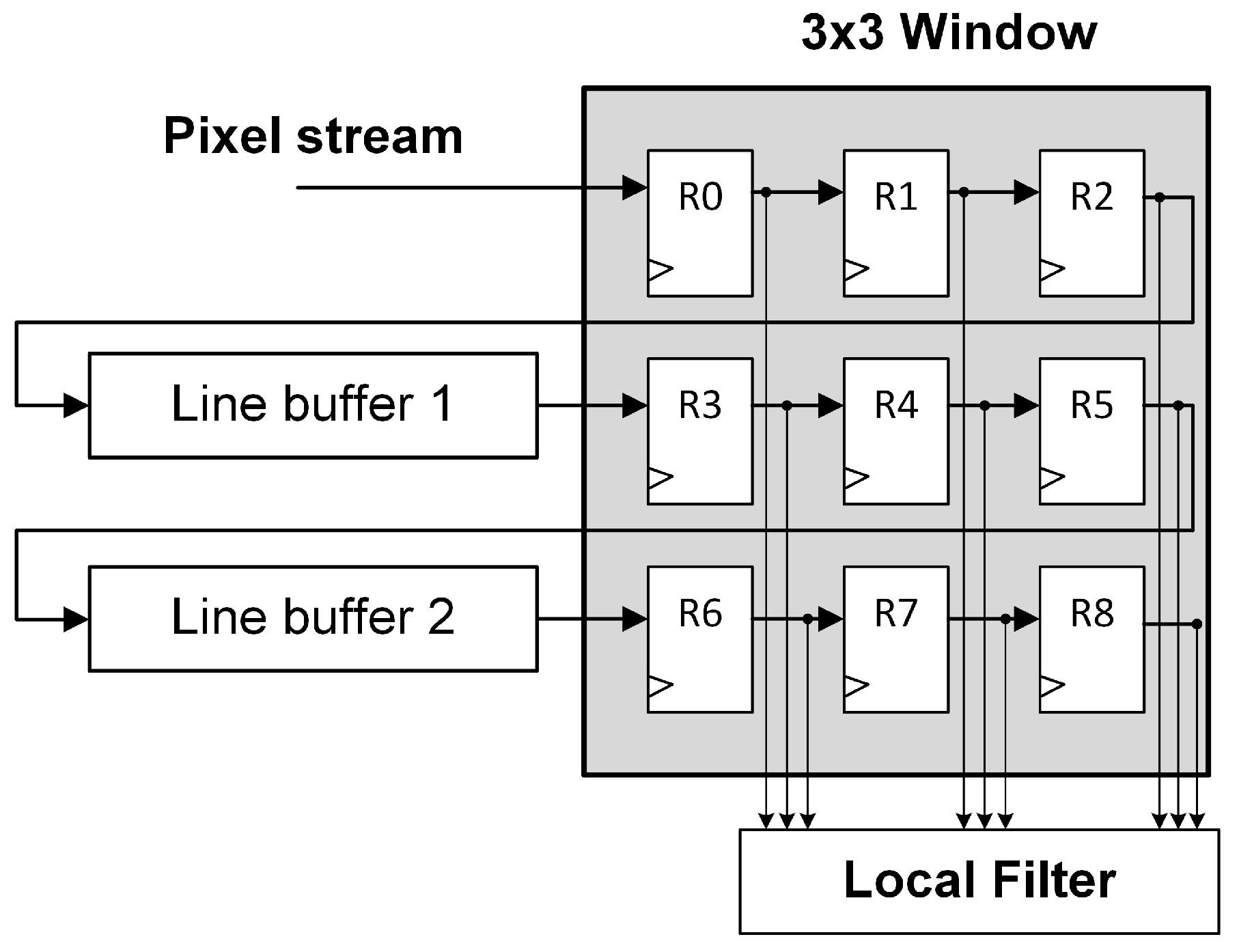
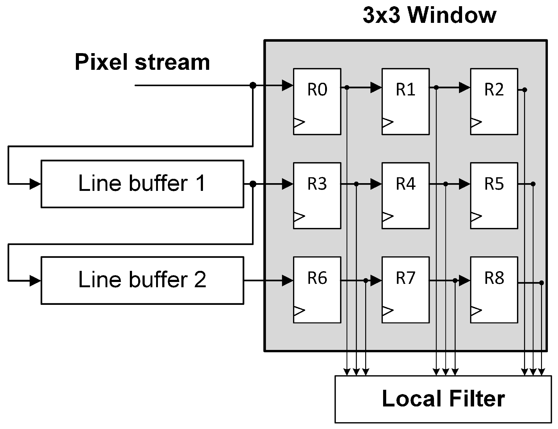
N pixel stream that sequentially passes through the local filter. In other words, moving the window along the image is equivalent to streaming the image through the window. This procedure is commonly known as pixel caching, and it is based on the fact that each pixel is reused in multiple window positions. There are several pixel caching structures [
13], but they all consist of line buffers and registers. The main difference between those structures is how the connections of the mentioned line buffers are performed. FIFO line buffers can be connected in series or in parallel with the window as shown in
Figure 2 and
Figure 3.
The structures presented in
Figure 2 and
Figure 3 are functionally equivalent. They temporarily store the pixel stream in order to enable a 3 × 3 local filter operation. As can be noticed, these structures does not deal with the image borders. For instance, those pixels at the end of a row are followed by the pixels at the beginning of the next row. Therefore, the border pixels will usually be invalid. There are several approaches to deal with border pixels such as duplication, mirroring with duplication, or mirroring without duplication [
13]. However, the original structures presented in
Figure 2 and
Figure 3 have been studied since, in most applications, the useful information in the image is typically located in the center of the image.
In order to test both line-buffer-based pipelines, a standard 8-bit 128 × 128 pixels grayscale image has been chosen (see
Figure 4). As will be explained later, the presented protection techniques are independent of the image size, so the relative resource overhead added to protect the original design decreases as the image size increases. Therefore, a reasonably small image size has been chosen to evaluate the pipelines in a realistic but unfavourable case scenario.
The standard Lena image in
Figure 4 has been selected to test the pipelines because its grayscale properties make it widely used in the image processing field [
14]. The size of the line buffers and registers is dependent on the image color depth, so for an 8-bit grayscale image, the size of both line buffers and registers must be 8-bits. If, for example, a three-channel RGB color image was used, the pipelines would have to be replicated in parallel for each channel. Then, the proposed error detection scheme can be used to individually protect each of them. This protection technique is presented below.
3. Proposed Techniques
As mentioned in the Introduction, configuration memory errors in SRAM-based FPGAs modify the design functionalities permanently until the original bitstream is reloaded. For this reason, it is more practical to detect the error and then perform a partial or complete reconfiguration of the device to rewrite the affected configuration bits. In contrast to complete reconfiguration, partial reconfiguration avoids reloading the whole bitstream on the device by changing parts of the configuration memory frames while the FPGA is working, so the application does not have to be stopped [
15]. Therefore, protection techniques that provide enough information about the damaged part of the design are helpful in facilitating the partial reconfiguration of the device.
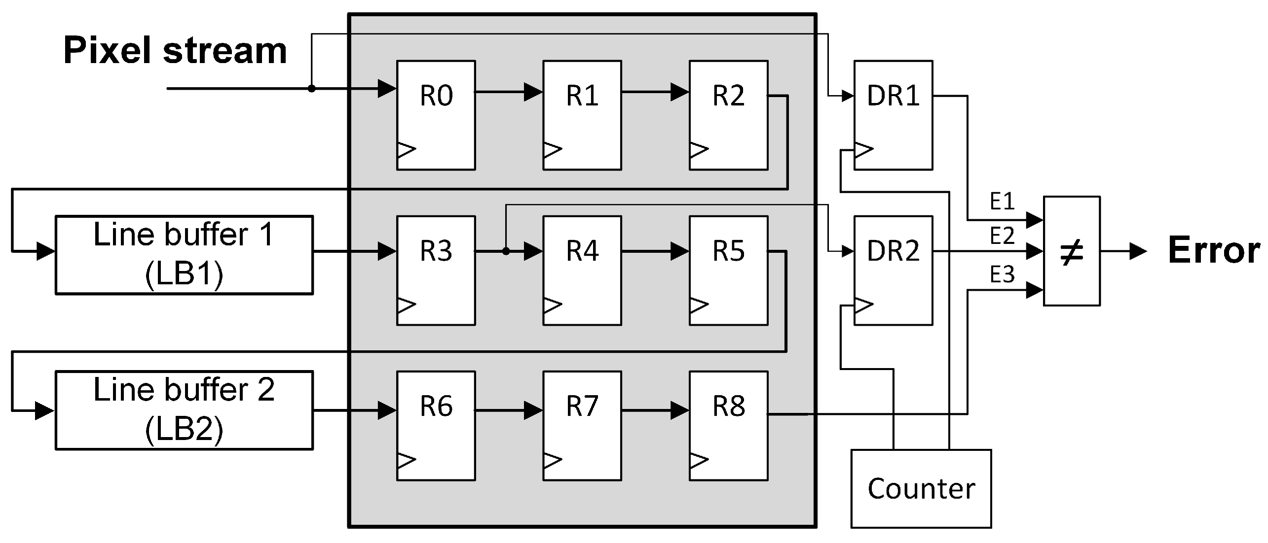
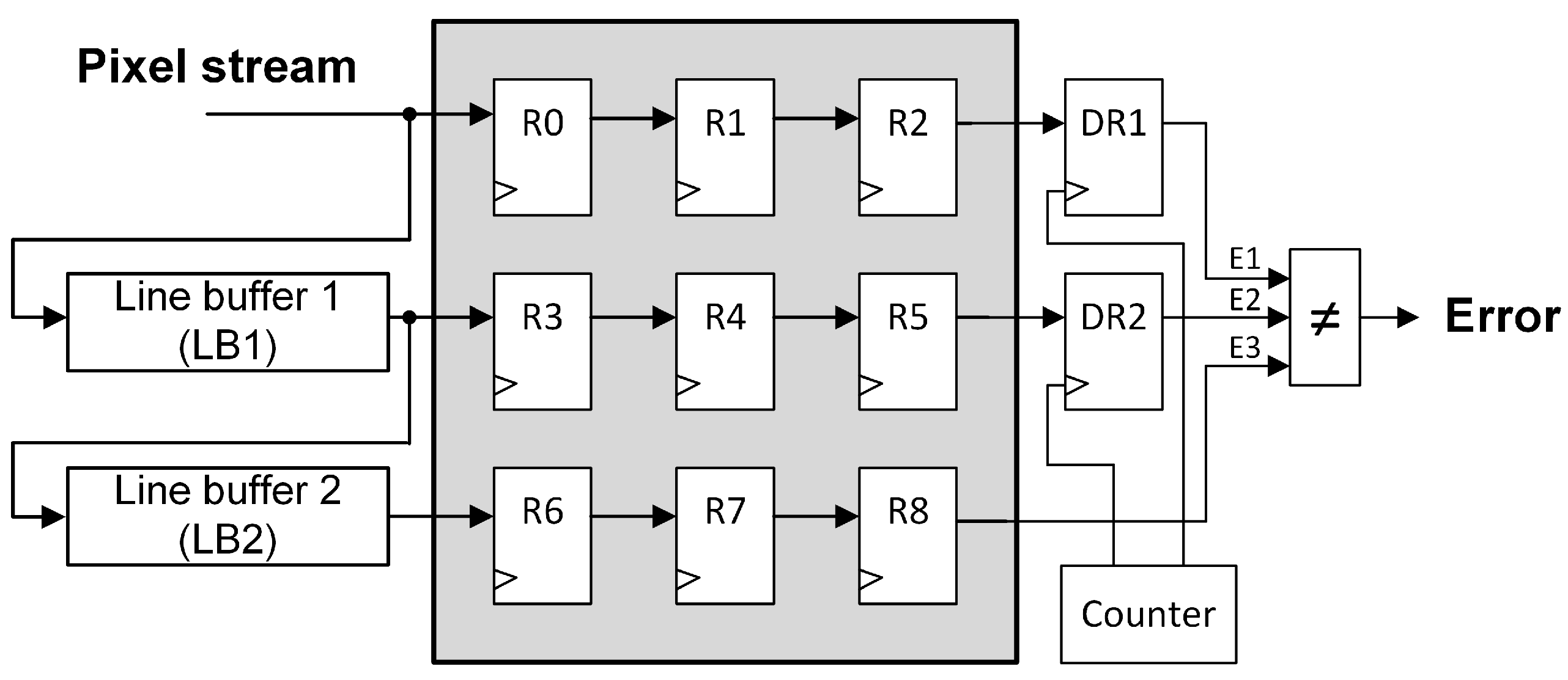
Figure 5 illustrates the proposed protection technique for the series structure shown in
Figure 2, while the protected parallel structure is presented in
Figure 6 (output register connections to “Local Filter” block have been omitted for a better visualization). As can be observed, both techniques are based on including a couple of 8-bit detection registers (
DR1 and
DR2), a counter, and a three-input comparator to the original unprotected design.
It should be noticed that both error detection registers are different from the window registers. Every register in
Figure 5 and
Figure 6 is a synchronous 8-bit register, but
DR1 and
DR2 are also controlled by a pixel counter that enables the reading/writing operations. This mechanism is needed to perform the comparison of the three output signals (
E1,
E2, and
E3) at some particular time periods. For example, in the protected parallel pipeline, the pixel at time
t is stored in
R0 and
LB1, then, at time (
) this pixel is stored in
DR1. The same pixel will be stored in
DR2 at (
+
line buffer length), and will be outputted by
R8 (
line buffer length) clock cycles later. At this precise moment, the error signals comparison has to be performed to detect if a configuration memory error has modified the pixel value during its travel through the pipeline. Therefore, for the selected 128 × 128 pixels grayscale image, one pixel every
clock cycles is checked. The proposed error detection technique is based on the fact that a configuration memory error modifies permanently the configuration of the design, so once the error has damaged the pipeline, most of the subsequent pixel values will be corrupted.
As can be observed in
Figure 5 and
Figure 6, the error detection registers have been connected to different parts of the pipelines. The series structure is a long unique delay line, so the connections are at the beginning, the middle, and the end of the pipeline in order to check if the pixel has been corrupted during its trip through the pipeline. In the parallel structure, the connections have been made at the end of the branches to detect errors in each of them. These connections also enable the identification of the damaged part of the pipeline. Using the three error detection output signals
E1,
E2, and
E3, a table can be created to evaluate the different possible scenarios and the part of the design that has to be reconfigured to remove the configuration memory error. These errors affect equally both logic elements and routing, so the partial reconfiguration has to be performed in the damaged components shown in
Table 1 and their route-related configuration bits. Moreover, the counter always has to be reconfigured along with the possible damaged parts of the pipeline since all the erroneous output scenarios can be caused by an error on it.
Table 1 summarizes the possible damaged parts of the studied pipelines depending on the values of the output error detection signals. For example, in the series pipeline, if a configuration memory error affects the window register
R4, then the pixels stored in
DR1 and
DR2 will be equal, but the pixel could be corrupted as it passes through
R4, so the pixel that outcomes from
R8 may not be equal to them. This means that
E1 and
E2 would have the same values but
E3 would be different from them. Conversely, the same scenario in the parallel pipeline means that only
DR2 would store a different value since the output of
R5 is not connected to the rest of the pipeline, so
E2 would have a different value from
E1 and
E3. The rest of the scenarios presented in
Table 1 can be similarly deduced. With the information provided in
Table 1, a partial reconfiguration of the damaged part of the pipeline can be performed to remove the error, instead of reconfiguring the entire FPGA. The quantitative benefits of partial reconfiguration against complete reconfiguration are not discussed in this paper, but they are considered as future work.
4. Technique Evaluation
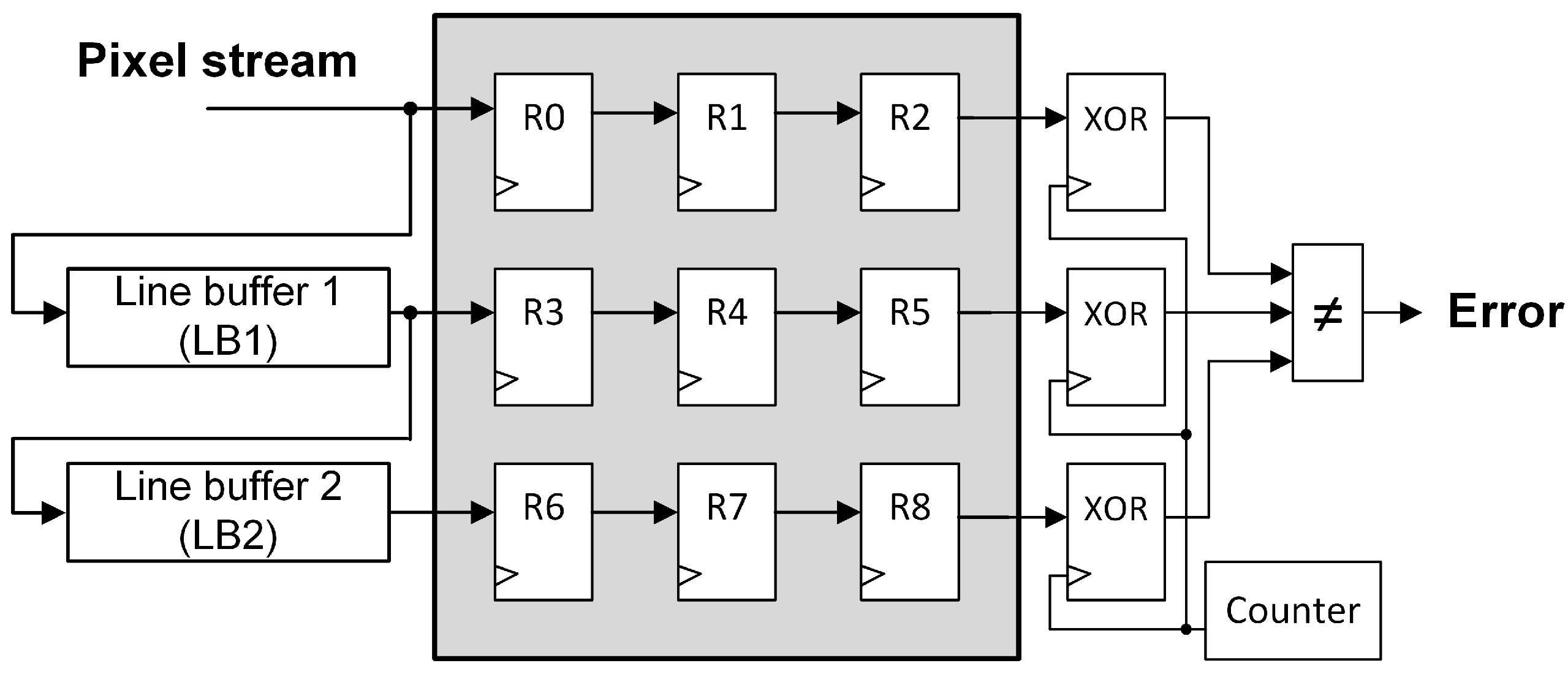
In order to compare performance in terms of resource utilization and error detection rate, an XOR-based signature technique has been chosen. This technique creates a signature of the input image using an XOR gate and a couple of 8-bit registers. The input image pixels are XORed and the result is stored for a later comparison to the similarly calculated output pixels signature. If an error alters the pixel values that pass through the pipeline, a signature mismatch occurs and the error is detected. The described XOR-based signature calculation module is shown in
Figure 7. In this figure,
Reg 1 is a simple 8-bit synchronous register, however,
Reg 2 also uses a read/write enable signal controlled by a counter to temporarily store the signature, as happened with the error detection registers
DR1 and
DR2 from the proposed techniques.
This module (named “XOR” in
Figure 8 and
Figure 9) has to be placed before and after the series pipeline to calculate the input and the output image signatures for later comparison. However, in the parallel pipeline, three XOR modules have to be used to be able to detect errors in the three pipeline branches. This connection is similar to the one performed in
Figure 6 for the proposed technique.
The proposed error detection structures presented in
Section 3 and the XOR-signature technique have been implemented in the SRAM-based FPGA part of a Xilinx Zynq-7000 All Programmable System on a Chip (SoC) obtaining the utilization reports presented in
Table 2 and
Table 3.
In
Table 2, the number of look-up tables (LUTs) and flip-flops (FFs) used by each series structure is presented, while the parallel pipeline resources are shown in
Table 3. The percentages in these tables show the overhead of LUTs or FFs added to the unprotected design to implement each protection technique. In the parallel structure, the XOR-based scheme needs three XOR signature generation modules so, as can be observed in
Table 3, significantly more resources are required. In the series pipeline, the number of LUTs is slightly higher in the proposed technique. This is due to the use of a two-input comparator in the XOR-based scheme instead of a three-input comparator but, in general, the total FPGA resource usage of the proposed technique is lower.
The error detection rate of the techniques has been measured through fault-injection. First, the techniques are validated against the standard 8-bit grayscale Lena image presented in
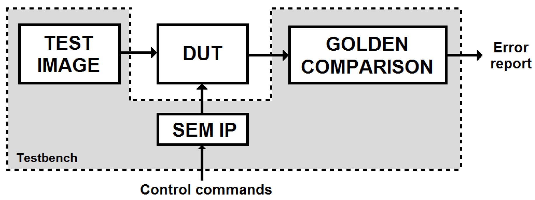
Figure 4 to obtain the “golden” output pixel values that should outcome from the pipeline if no error is injected. These golden outputs are then stored for later golden comparisons. Once the golden outputs are obtained, an exhaustive fault-injection campaign is executed using the Xilinx Soft Error Mitigation (SEM) IP Controller [
16]. The SEM IP is an independent circuit that has to be loaded along with the design under test (DUT) in order to perform read/write operations in the DUT-related configuration bits through the internal configuration access port (ICAP). The fault-injection campaign is sequentially performed in an injection-correction loop. In each iteration, a configuration bit is flipped, the test image is processed, and the golden comparison results are stored. Finally, the bit flip is corrected by the SEM IP and the loop is repeated until all the DUT-related configuration bits are covered. It is worth mentioning that SEUs have been injected since they are the worst case scenario for the error detection techniques considered in this paper. This is because more errors imply more opportunities to detect a malfunction in the pipeline.
For a better understanding of the experimental set-up, the fault-injection framework is presented in
Figure 10. This figure illustrates the different modules that are loaded in the SRAM-based FPGA. Those modules that are grouped together inside the grey-shaded “Testbench” box are not affected by the fault injector.
The fault-injection campaign has been performed for the unprotected original design, the XOR-based protection scheme, and the proposed protection technique, obtaining the results summarized in
Table 4 and
Table 5.
Table 4 presents the error detection capabilities for the series structure of the line-buffer-based pipeline, while
Table 5 shows the results for the parallel pipeline.
It can be observed in these tables that the detection rate is approximately the same in both pipelines and between both studied techniques. However, the proposed technique seems to be more effective than the XOR-based scheme due to its fewer false positives. This is particularly noticeable in the parallel pipeline, in which the percentage of false positive detections is more than twice the proposed technique. False positives are strongly related to the number of FPGA resources used for the error detection part, so an error affecting these configuration bits can trigger the “error detected” signal while the pipeline outputs are still correct. By comparing
Table 2 and
Table 3, it can be noticed that the XOR-based scheme requires more LUTs and FFs for the parallel pipeline than for the series pipeline since it needs a third XOR module to perform the error detection. As can be observed in
Table 5, these additional resources imply more false positive detections that will lead to more FPGA reconfigurations. Consequently, the availability of the FPGA will be increased when our proposed technique is implemented.
In order to measure the quality of the outputted image when the error is not detected, the averaged Mean Square Error (MSE) of the undetected corrupted images has also been calculated for each pipeline scheme and included in
Table 4 and
Table 5. It can be observed that there is a significant reduction of the MSE in both protection schemes compared to the unprotected pipelines and that the averaged MSE obtained for the proposed protection schemes is slightly lower than the XOR-based technique. This means that, when an error is not detected by our proposed technique, the outputted corrupted image will still have (on average) better quality than the image outputted by the XOR-based scheme and, therefore, it should have a lower impact on subsequent image processing algorithms.
5. Conclusions and Future Work
In this paper, a novel method to protect line-buffer-based image processing pipelines against SRAM-based FPGA configuration memory errors is presented. Our proposed method is used to protect two types of line-buffer pipelines (series and parallel). They store the image pixels temporarily using two additional 8-bit registers. These pixels are later compared and, if a pixel mismatch is found, the error is detected and then a partial or complete reconfiguration can be performed.
The proposed technique has been compared in terms of FPGA resource usage and error detection rate with an XOR-based signature scheme commonly used to protect pipelines. Both detection techniques have been implemented in a Xilinx SRAM-based FPGA and fault-injection campaigns have been performed using a Xilinx injection IP core.
Experimental results show that the proposed technique presents lower FPGA resource usage, similar error detection rate, and fewer false positive detections in comparison with the XOR-based scheme. In addition to this, the proposed technique has also been designed in a manner that the identification of the damaged part of the pipeline can be easily inferred, so the partial reconfiguration of the damaged module is facilitated. This means that, using our proposed error detection method, the image processing system does not have to be stopped and rebooted, as usually happens when a classic complete reconfiguration is performed. Implementing and measuring the effectiveness of the partial reconfiguration in terms of time and power consumption is considered as future work.


