Article

A Novel High-Performance Low-Cost Double-Upset Tolerant Latch Design

1
State Key Laboratory of Functional Materials for Informatics, Shanghai Institute of Microsystem and Information Technology, Chinese Academy of Sciences, Shanghai 200050, China
2
University of Chinese Academy of Sciences, Beijing 100049, China
3
Shanghai Huahong Grace Semiconductor Manufacturing Corporation, Shanghai 201203, China
*
Author to whom correspondence should be addressed.
Electronics 2018, 7(10), 247; https://doi.org/10.3390/electronics7100247
Submission received: 23 August 2018 / Revised: 4 October 2018 / Accepted: 10 October 2018 / Published: 12 October 2018
(This article belongs to the Section Microwave and Wireless Communications)

Abstract

:
Single event double upsets (SEDUs) caused by charge sharing have been an important contributor to the soft error in integrated circuits. Most of the up-to-date double-upset (DU) tolerant latches suffer from high costs in terms of delay, power and area. In this paper, we propose a novel high-performance low-cost double-upset tolerant (HLDUT) latch. Simulation waveforms have validated the double-upset tolerance of the proposed latch. Besides, detailed comparisons demonstrate that our design saves 805.24% delay-power-area product (DPAP) on average compared with other considered up-to-date double-upset tolerant latches, which means the proposed latch is a promising candidate for future highly reliable low-cost applications.

1. Introduction

With technology advancing, the charge needed to trigger the upset of the logic state of a circuit node has dramatically decreased due to the scaling of supply voltage and the reduction of the internal node capacitance, making the circuit more vulnerable to single-event effects (SEEs) [1,2,3]. SEEs have caused severe reliability problems in large-scale integration (LSI) systems for both aerospace and terrestrial applications. When a high-energy particle hits a silicon-based circuit system, electron-hole pairs generated along its trail in the silicon will be separated and collected if the trail is in close proximity to the depletion region [4]. If the charge collected is sufficient to upset the original logic state of the struck node, a large current/voltage transient fault (TF) can be generated. With regard to a combinational logic circuit, the TF produced in it is viewed as single event transient (SET). Worse still, when a TF transmitted from a combinational logic circuit is captured in a latch or flip-flop, it will be a single event upset (SEU) and thus a soft error is produced. Besides, an SEU can also be created directly in a sequential circuit [5].
Since the traditional latch shown in Figure 1 can be easily upset by an SEU and cannot recover itself, a number of robust latches have been reported to deal with the single-event upset (SEU) [6,7,8]. Applying dual modular redundancy or dual-interlocked storage cell (DICE) [6], HiPeR (High Performance Robust) latch presented in [7], and HLR-CG1 (High performance, Low cost and Robust Clock Gating) latch proposed in [8] can tolerate the disturbance of SEU. However, for advanced CMOS technologies, the proximity of devices by scaling can result in charge collection and sharing at multiple nodes from a single high-energy particle strike [9]. These existing schemes proposed for tolerating SEU or single upset (SU) can no longer be robust in face of double upsets (DUs). Well isolation, guard rings and layout techniques were utilized to solve the multiple upsets caused by charge sharing, but benefits of these techniques are quite limited [9,10]. In order to solve this severe problem, researchers have proposed plenty of latches which can effectively tolerate the DUs [11,12,13,14,15,16,17]. The latch designed in [12] employed a modified triple path dual-interlocked storage cell (TPDICE) [11] and Muller C-element (MCE), acquiring better tolerance. As for DNCS (Double-Node Charge Sharing) latch in [13] and CLCT (Circuit and Layout Combination Technique) latch in [14], both latches utilized interlocked structure and MCE to obtain the robustness. However, the latch in [14] was not fully SEDU tolerant in the circuit design level, and further, layout technique was used to harden the latch. The Delta DICE in [15], DONUT (Double Node Upset Tolerant) in [16], and DNURL (Double-Node-Upset-Resilient Latch) in [17] were derived by the applications of feedback loop. However, it is worth noticing that these latches were carried out with large cost penalties in terms of delay, power consumption and area.
In this paper, a novel high-performance low-cost double-upset tolerant (HLDUT) latch is proposed. It utilizes a high-speed transmission path to get high performance, and clock gating (CG) to acquire low-power consumption property. Furthermore, inverters 2P1N and 1P2N, and clocked three-input MCE are employed to tolerate the soft error. In Figure 2, the schematic and symbol of the inverters 2P1N and 1P2N, and clocked three-input MCE are portrayed. If the A and B in 2P1N inverter are in different logic states, the pull-up network will be disabled. Similarly, if the B and C in 1P2N inverter are in different logic states, the pull-down network will be turned off.
The rest of the paper is organized as follows. Section 2 presents the structure, behavior, implementation and verification of the proposed HLDUT latch. In Section 3, detailed comparisons between the proposed and the referential latches are carried out. Conclusions are given in Section 4.

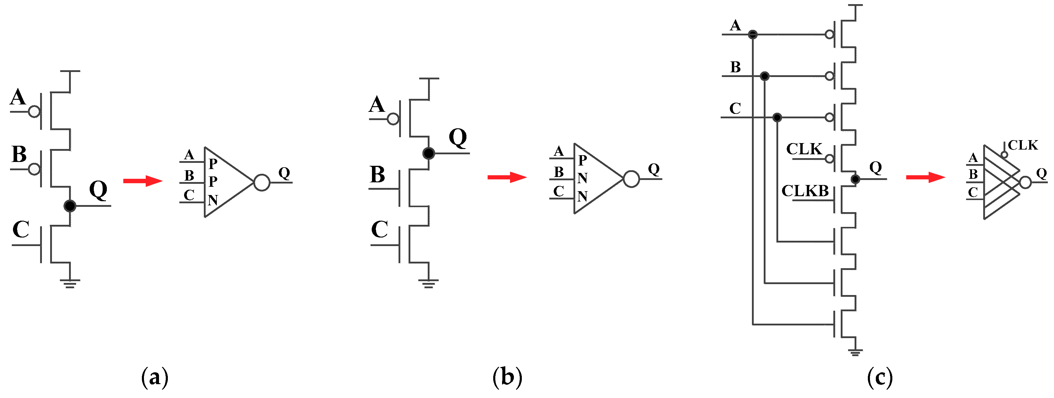
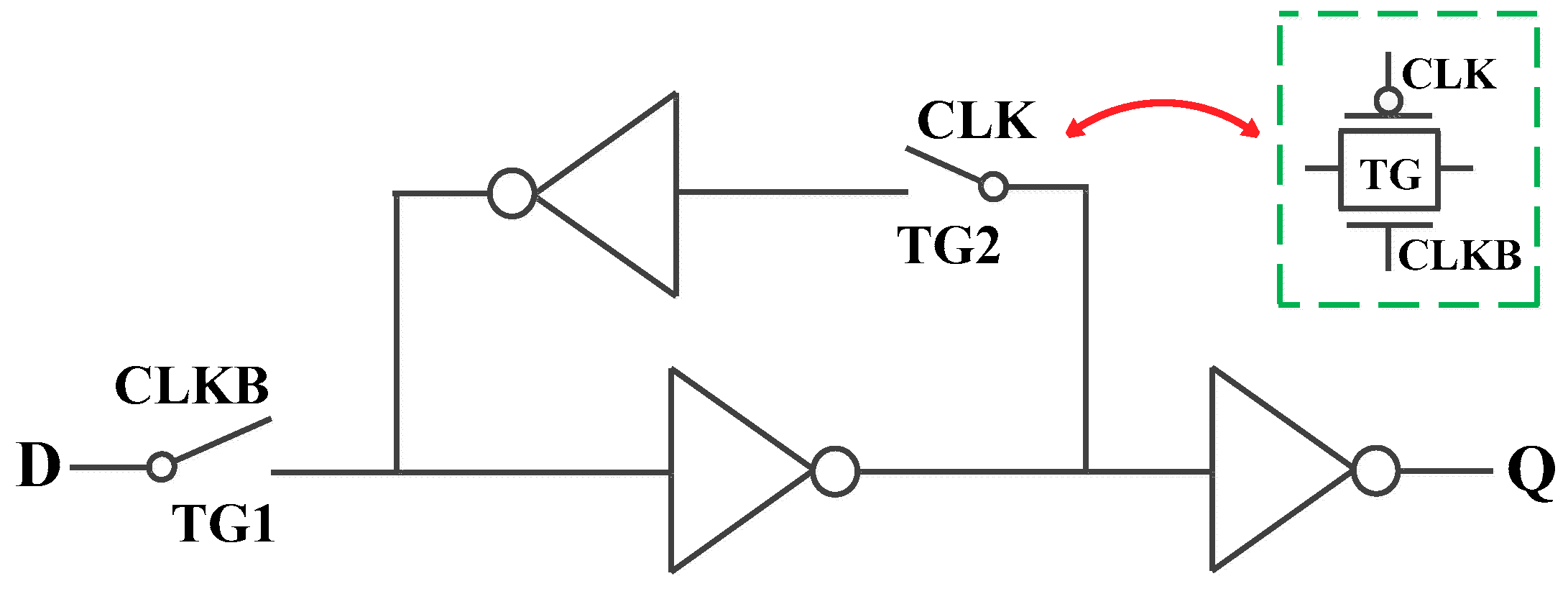
2. Proposed HLDUT Latch

2.1. Circuit Structure and Behavior

As is shown in Figure 3, the proposed HLDUT latch is constructed from a novel storage cell, a clocked three-input MCE, and four transmission gates (TG), TG1–TG4. The storage cell comprises three clocked 2P1N inverters (I1, I3 and I5), and three 1P2N inverters (I2, I4 and I6). By connecting input port D and output port Q through TG4, a high-speed path is created.
When the clock signal CLK is at a high logic state and CLKB is at the low, the latch is in transparent mode. TG1–TG4 are turned on, I1, I3 and I5 are disabled, and the clocked three-input MCE is turned off. Signal at the input port will be transmitted to the output port Q, and the internal nodes of the storage cell, biasing the logic states of the other storage nodes. In this case, the delay time from input D to output Q is also optimized because of the current competition is prevented at the output Q due to the three-input MCE being disabled. Besides, power dissipation can be cut down by preventing the current competitions at the outputs of the inverters I1, I3 and I5. When D = 0, S1, S3 and S5 are set to 0, and further S2, S4 and S6 are biased to 1. In this case, 0 will be obtained at the output. When D = 1, S1, S3 and S5 are set to 1, and further S2, S4 and S6 are biased to 0. Then the output will be in high logic state.
When CLK is set to be low and CLKB is biased to be high, the latch is in hold mode. TG1–TG4 are turned off, and inverters I1, I3, I5 and the clocked three-input MCE are enabled. The signals at output Q are determined by the data propagating from the storage cell.
In the presence of soft error in the hold mode, different cases are discussed. When a single node inside the storage cell is affected by an SEU, the soft error will not be transmitted to the output because of the block of the MCE and the node affected will soon be biased to its right logic state. In case of DUs affecting a pair of nodes inside the latch, there are two possible cases. Case1: a node inside the storage cell and Q are affected. In this case, the storage cell works the same as the case where a single internal node is affected, and the output Q will restore its right logic state. Case 2: two nodes inside the storage cell are affected.
As for case 2, C62 = 15 different node pairs can be found. Assume SX represents the internal nodes. From the internal connections, these node pairs can be classified into three categories:
(1)
<SX, SX+1>: <S1, S2>, <S2, S3>, <S3, S4>, <S4, S5>, <S5, S6>, <S6, S1>;
(2)
<SX, SX+2>: <S1, S3>, <S2, S4>, <S3, S5>, <S4, S6>, <S5, S1>, <S6, S2>;
(3)
<SX, SX+3>: <S1, S4>, <S2, S5>, <S3, S6>.
Besides, they can also be sorted into two types according to the two distinct tolerant mechanisms of the proposed latch. Type 1: the storage cell is resilient from the feedback when affected by DUs. Type 2: the storage cell cannot recover itself when a pair of internal nodes is upset, but the clocked three-input MCE will block the soft error.
Assuming D = Q = 1 before the change of CLK from 1 to 0, we get S1 = S3 = S5 = 1, and S2 = S4 = S6 = 0.
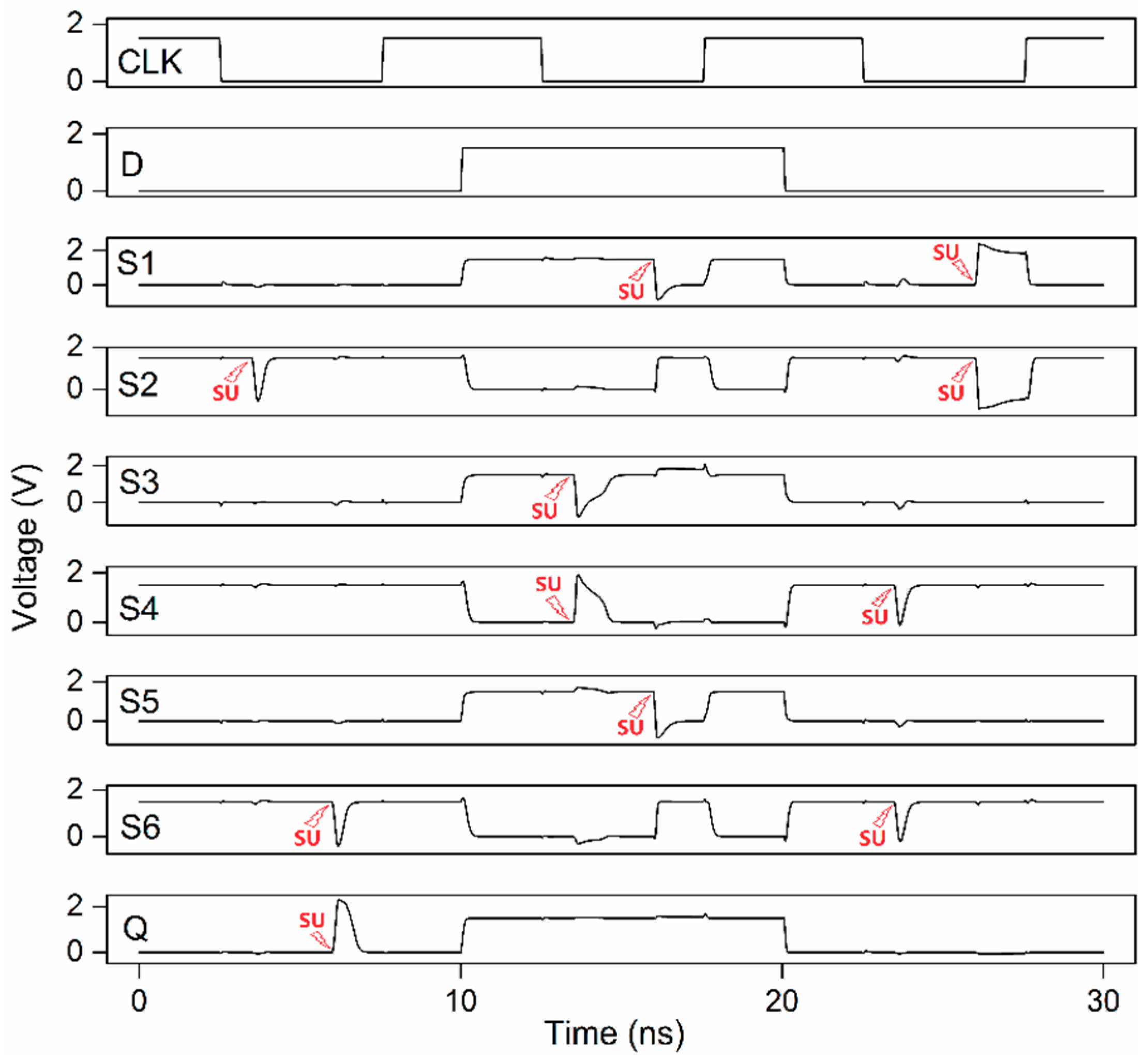
  • At first, we take the upset of node pair <S1, S2> in (1) into consideration. If nodes S1 and S2 are affected (i.e., S1 is discharged to 0 and S2 is charged to 1), the NMOS biased by S2 in I1 and the PMOS in I2 are turned on, while the PMOS transistors biased by S2 in I3 and I5, and the NMOS transistors biased by S1 in I4 and I6, are turned off. Since I3 and I5 are 2P1N inverters, and I4 and I6 are 1P2N inverters, S3, S4, S5 and S6 will be in high impedance state and their logic state will be kept temporarily. Thus, the PMOS and NMOS transistors in I1 and I2 are turned on, S1 and S2 will be unstable. The storage nodes except for S1 and S2 are not affected, thus S1 will be biased by S4 and S6 to its original logic 1 state, while S2 will be biased by S5 and S3 to its original logic 0 state. In this situation, node pair <S1, S2> belongs to type 1. Analyses are similar to that of node pairs <S3, S4> and <S5, S6> when they are affected by DUs, which means they belong to type 1.
  • If node pair <S2, S3> is affected by DUs (i.e., S2 is charged to 1 and S3 is discharged to 0), the NMOS biased by S2 in I1 and the PMOS in I4 are turned on, while the PMOS transistors biased by S2 in I3 and I5, and the NMOS transistors biased by S3 in I2 and I6, are turned off. Due to the fact that the PMOS and NMOS transistors in I1 and I4 are turned on temporarily, S1 and S4 are unstable. If the DUs are strong to upset the S1 and S4, the nodes S1, S2, S3 and S4 are affected, and they cannot recover to their original logic states. The PMOS transistors biased by S4 and S2 in I5 and the NMOS transistors in I6 are turned off, making S5 and S6 get into high impedance state and their logic state will be kept. Since S2, S4 and S6 are not in the same logic state, the soft error will be blocked by the clocked three-input MCE. The output Q is not affected, and the right logic state is maintained. Hence, node pair <S2, S3> belongs to type 2. Analyses are similar to that of node pairs <S4, S5>, <S6, S1>, and all of the node pairs in (2) and (3) when they are affected by DUs, which means they all belong to type 2.
In the case where D = Q = 0 before the change of CLK from 1 to 0, analyses are similar to that of the situation when D = Q = 1, and the latch retains its correct data at output Q in face of DUs. In this situation, node pairs <S1, S2>, <S3, S4> and <S5, S6> belong to type 2, while the other 12 node pairs belong to type 1.

2.2. Implementation and Verification

The proposed HLDUT latch has been implemented in 110 nm CMOS technology of HHGrace. The nominal supply voltage for this process is 1.5 V. With regard to the transistor sizes in the design, they are listed as follows: (1) for the storage cell and TG1–TG3, the PMOS and NMOS transistors are set to W/L = 800/120 nm and W/L = 230/120 nm, respectively; (2) for the clocked three-input MCE and TG4, the PMOS and NMOS transistors are set to W/L = 1.16 µm/120 nm and W/L = 770/120 nm, respectively. Post-layout simulations have been performed with HSPICE. A double-exponential current source, the rise and fall time constants of which are set to 50 and 164 ps respectively, has been utilized in the simulations [7,8,12,17,18,19]. To validate the SU and DU tolerance, the injected charge of the worst case is chosen to be up to 342 fC for a single upset.
From the simulation results in Figure 4, it can be seen that the proposed HLDUT latch has the same basic function with the traditional latch presented in Figure 1. At 3.5 ns, an SU is applied on node S2, and at 6 ns, 13.5 ns, 16 ns, 23.5 ns and 26 ns, two simultaneous SUs are applied on node pairs <S6, Q>, <S3, S4>, <S1, S5>, <S4, S6> and <S1, S2> respectively. The simulation results demonstrate that the proposed HLDUT latch can effectively tolerant SU and DUs. As shown in Figure 4, when node pair <S6, Q> is affected by DUs at 6 ns (i.e., S6 is discharged to 0 and Q is charged to 1), the PMOS transistors biased by S6 in I1 and I3 are turned on, while the NMOS biased by S6 in I5 is turned off. Since S4 and S2 are not affected and I1 and I3 are 2P1N inverter, the soft error will be blocked by the pull-up network of I1 and I3. Besides, S5 will be in a high impedance state and its logic state will be kept temporarily. Therefore, the storage nodes except for S6 are not affected; thus, S6 will be biased by S5 to its original logic 1 state. Finally, Q will be biased by the clocked three-input MCE to its original logic 0 state. Considering that the DU recovery analyses have been given in the former section in the case where D = Q = 1, we will focus on the case where D = Q = 0. When node pair <S4, S6> is affected by DUs at 23.5 ns (i.e., S4 and S6 are discharged to 0), the PMOS transistors biased by S4 in I1 and I5, and the PMOS transistors biased by S6 in I1 and I3 are turned on, while the NMOS transistors biased by S4 and S6 in I3 and I5 respectively, are turned off. Since S2 is not affected, and I3 and I5 are 2P1N inverters, S3 and S5 will be in high impedance state and their logic state will be kept temporarily. From the simulation waveform, we find S1 is affected by a small glitch and it recovers soon to its original logic 0 state. Finally, S4 and S6 are biased by S3 and S5, respectively, to the original logic 1 state. When node pair <S1, S2> is affected by DUs at 26 ns (i.e., S1 is charged to 1 and S2 is discharged to 0), the NMOS transistors biased by S1 in I4 and I6, and the PMOS transistors biased by S2 in I3 and I5 are turned on, while the NMOS transistor biased by S2 in I1 and the PMOS transistor biased by S1 in I2 are turned off. Since I3 and I5 are 2P1N inverters, and I4 and I6 are 1P2N inverters, S3, S4, S5 and S6 will be in high impedance state and their logic state will be kept temporarily. However, S1 and S2 cannot recover to their original logic state. Since S2, S4 and S6 are not in the same logic state, the soft error will be blocked by the clocked three-input MCE. The output Q is not affected, and the right logic state is maintained.
In addition, we also try to obtain the critical charge (Qcrit) for our proposed latch through HSPICE simulation. Upset cases in Figure 4 are reconsidered and 10 pC injected charge is given to every SU. It is observed that the output of the proposed HLDUT latch still keeps its right logic states under these extreme conditions. This result demonstrates that it is the number of upsets rather than the injected charge that dominate the SU and DU tolerance of the proposed HLDUT latch. Our former analyses of the SU and DU tolerance also support this point of view. It is worth noting that the rise and fall time constants applied in the simulations are not accurate parameters. From the simulated result that the output of the proposed HLDUT latch still keeps its right logic states when every SU in Figure 4 is given 10 pC, we can find that the rise and fall time constants, which are the important factors for the injected charge, are not key in our design. However, for the circuits hardened by combining the layout placement or increasing the critical charge, the rise and fall time constants should be simulated further to get more accurate results to validate the robustness of the circuits.

3. Evaluation

To compare fairly, all the considered latches are implemented by similar conditions and transistor sizes. The cost evaluations, with respect to delay time, power dissipation, area and delay-power-area product (DPAP), of the proposed latch and referential latches are presented in Table 1. The delay time is calculated by the average of the rise and fall delay from the input D to the output Q. With regard to the power dissipation, it is evaluated by a 50% input switching activity. The area is derived by equivalent unit size transistors (UST) [12,13,17]. DPAP is obtained by
DPAP = Delay × Power × Area.
As it stands, our proposed HLDUT latch has the lowest delay, thanks to the application of the high-speed path. For the same token, DNURL [17] also obtains a low delay. Even though HLR-CG1 [8] employs a high-speed transmission gate, it still suffers from a higher delay because there is current competition at its output. The SU tolerant latch HiPeR [7] features the lowest power dissipation and DPAP among all the other considered latches. With regard to those DU (let alone SU) tolerant latches, the proposed HLDUT latch exhibits the lowest power dissipation and DPAP while CLCT [14] has the lowest area.
To get detailed comparisons, the relative overheads in terms of delay, power, area and DPAP are presented in Table 2 ΔD shows the relative delay comparisons between the proposed HLDUT latch and other considered latches. Similarly, we can get the meaning of the ΔP, ΔA, and ΔDPAP. Δ is calculated by
Δ = [(compared latch − proposed latch)/proposed latch] × 100%.
As is presented in Table 2, the proposed HLDUT latch saves 191.2%, 53.6%, 80.2%, 760.7%, 470.0%, 270.8%, 342.9% and 8.8% delay compared with the traditional, HiPeR [7], HLR-CG1 [8], DNCS [13], CLCT [14], Delta DICE [15], DONUT [16] and DNURL [17], respectively. Compared with other DU (let alone SU) tolerant latches, the proposed HLDUT latch is also a power-efficient design, even though it exhibits 25.6% and 27.6% power penalty over the traditional and HiPeR [7]. Besides, it can be derived that area penalty is inevitable if we want better soft error tolerance. Nevertheless, the proposed high-performance low-cost double-upset tolerant latch saves 805.24% DPAP on average compared with other considered up-to-date DU tolerant latches, which means it is a promising candidate for future highly reliable low-cost applications.

4. Conclusions

The technology scaling has made the single event double upsets (SEDUs) a severe reliability problem for both aerospace and terrestrial applications. Considering that most of the up-to-date double-upset tolerant latches suffer from high costs, we have presented a novel high-performance low-cost double-upset tolerant (HLDUT) latch in this paper. Simulation waveforms have validated the double-upset tolerance of the proposed latch. Besides, detailed comparisons demonstrate that our design saves 805.24% DPAP on average compared with other considered up-to-date double-upset tolerant latches, which means the proposed latch is a promising candidate for future highly reliable low-cost applications.

Author Contributions

J.J. contributed to the design, analysis and writing of the paper. W.Z., J.X., and S.Z. contributed to the overall study, simulation, and revision of the paper.

Funding

This research received no external funding.

Conflicts of Interest

The authors declare no conflict of interest.

References

  1. Narasimham, B.; Gupta, S.; Reed, D.; Wang, J.K.; Hendrickson, N.; Taufique, H. Scaling trends and bias dependence of the soft error rate of 16 nm and 7 nm FinFET SRAMs. In Proceedings of the IRPS, Burlingame, CA, USA, 11–15 March 2018. [Google Scholar]
  2. Bohr, M.T.; Yong, I.A. CMOS scaling trends and beyond. IEEE Micro 2017, 37, 20–29. [Google Scholar] [CrossRef]
  3. Ibe, E.; Taniguchi, H.; Yahagi, Y.; Shimbo, K.; Toba, T. Impact of scaling on neutron induced soft error in SRAMs from an 250 nm to a 22 nm design rule. IEEE Trans. Electron Devices 2010, 57, 1527–1538. [Google Scholar] [CrossRef]
  4. Ferlet-Cavrois, V.; Massengill, L.W.; Gouker, P. Single event transients in digital CMOS—A review. IEEE Trans. Nucl. Sci. 2013, 60, 1767–1790. [Google Scholar] [CrossRef]
  5. Baumann, R.C. Radiation-induced soft errors in advanced semiconductor technologies. IEEE Trans. Device Mater. Rel. 2005, 5, 305–316. [Google Scholar] [CrossRef]
  6. Calin, T.; Nicolaidis, M.; Velazco, R. Upset hardened memory design for submicron CMOS technology. IEEE Trans. Nucl. Sci. 1996, 43, 2874–2878. [Google Scholar] [CrossRef]
  7. Omana, M.; Rossi, D.; Metra, C. High-performance robust latches. IEEE Trans. Comput. 2010, 59, 1455–1465. [Google Scholar] [CrossRef]
  8. Nan, H.; Choi, K. High performance, low cost, and robust soft error tolerant latch designs for nanoscale CMOS technology. IEEE Trans. Circuits Syst. I Reg. Pap. 2012, 59, 1445–1457. [Google Scholar] [CrossRef]
  9. Balbekov, A.O.; Gorbunov, M.S.; Zebrev, G.I. Circuit-level layout-aware modeling of single-event effects in 65-nm CMOS ICs. IEEE Trans. Nucl. Sci. 2018, 65, 1914–1919. [Google Scholar] [CrossRef]
  10. Chen, R.; Zhang, F.; Chen, W.; Ding, L.; Guo, X.; Shen, C.; Luo, Y.; Zhao, W.; Zheng, L.; Guo, H.; et al. Single-event multiple transients in conventional and guard-ring hardened inverter chains under pulsed laser and heavy-ion irradiation. IEEE Trans. Nucl. Sci. 2017, 64, 2511–2518. [Google Scholar] [CrossRef]
  11. Blum, D.R.; Delgado-Frias, J.G. Schemes for eliminating transient width clock overhead from set-tolerant memory-based systems. IEEE Trans. Nucl. Sci. 2006, 53, 1564–1573. [Google Scholar] [CrossRef]
  12. Jiang, J.; Xu, Y.; Ren, J.; Zhu, W.; Lin, D.; Kong, W.; Zou, S. Low-cost single event double-upset tolerant latch design. Electron. Lett. 2018, 54, 554–556. [Google Scholar] [CrossRef]
  13. Katsarou, K.; Tsiatouhas, Y. Soft error interception latch: Double node charge sharing SEU tolerant design. Electron. Lett. 2015, 51, 330–332. [Google Scholar] [CrossRef]
  14. Hui, X.; Yun, Z. Circuit and layout combination technique to enhance multiple nodes upset tolerance in latches. IEICE Electron. Exp. 2015, 12, 1–7. [Google Scholar] [CrossRef]
  15. Eftaxiopoulos, N.; Axelos, N.; Zervakis, G.; Tsoumanis, K.; Pekmestzi, K. Delta DICE: A double node upset resilient latch. In Proceedings of the IEEE International Midwest Symposium on Circuits Systems, Fort Collins, CO, USA, 2–5 August 2015; pp. 1–4. [Google Scholar]
  16. Eftaxiopoulos, N.; Axelos, N.; Pekmestzi, K. DONUT: A double node upset tolerant latch. In Proceedings of the IEEE Computer Society Annual Symposium on VLSI, Montpellier, France, 10–15 July 2015; pp. 509–514. [Google Scholar]
  17. Yan, A.B.; Huang, Z.; Yi, M.; Xu, X.; Ouyang, Y.; Liang, H. Double-node-upset-resilient latch design for nanoscale CMOS technology. IEEE Trans. VLSI Syst. 2017, 25, 1978–1982. [Google Scholar] [CrossRef]
  18. Dharchoudhury, A.; Kang, S.M.; Cha, H.; Patel, J.H. Fast timing simulation of transient faults in digital circuits. In Proceedings of the IEEE/ACM International Conference on Computer-Aided Design, San Jose, CA, USA, 6–10 November 1994; pp. 719–722. [Google Scholar]
  19. Lu, Y.; Lombardi, F.; Pontarelli, S.; Ottavi, M. Design and analysis of single-event tolerant slave latches for enhanced scan delay testing. IEEE Trans. Device Mater. Reliab. 2014, 14, 333–343. [Google Scholar]
Figure 1. Schematic of the traditional latch. The switch is the symbol of the transmission gate (TG). When CLK = 1 and CLKB = 0, TG1 is turned on, and TG2 is turned off. When CLK = 0 and CLKB = 1, TG1 is turned off, and TG2 is turned on.
Electronics 07 00247 g001
Figure 2. Schematic and symbol of (a) 2P1N inverter; (b) 1P2N inverter; (c) three-input Muller C-element (MCE) with clock gating (CG).
Electronics 07 00247 g002
Figure 3. Schematic of the proposed HLDUT latch.
Electronics 07 00247 g003
Figure 4. Simulation waveforms for HLDUT latch.
Electronics 07 00247 g004
Table 1. Cost comparisons of all considered latches.
LatchSU Tolerant?DU Tolerant?Delay (ps)Power (μW)Area (UST)DPAP (×104)
The traditional××84.992.9149.61.23
HiPeR [7]×44.832.8391.91.17
HLR-CG1 [8]×52.615.4885.52.46
DNCS [13]251.246.91171.129.70
CLCT [14]166.395.05148.912.51
Delta DICE [15]108.2310.59198.622.76
DONUT [16]129.2810.31164.621.94
DNURL [17]31.766.89268.55.88
HLDUT29.193.91179.32.05
Table 2. Detailed cost comparisons between the proposed latch and other considered latches.
LatchΔDΔPΔAΔDPAP
The traditional191.2%−25.6%−72.3%−40.0%
HiPeR [7]53.6%−27.6%−48.7%−42.9%
HLR-CG1 [8]80.2%40.2%−52.3%20.0%
DNCS [13]760.7%76.7%−4.6%1348.8%
CLCT [14]470.0%29.2%−17.0%510.2%
Delta DICE [15]270.8%170.8%10.8%1010.2%
DONUT [16]342.9%163.7%−8.2%970.2%
DNURL [17]8.8%76.2%49.7%186.8%

