Abstract
In this paper, we extensively analyzed the drain-induced barrier lowering (DIBL) and leakage current characteristics of the proposed partial isolation field-effect transistor (PiFET) structure. We then compared the PiFET with the conventional planar metal-oxide semiconductor field-effect transistor (MOSFET) and silicon on insulator (SOI) structures, even though they have the same doping profile. Two major features of the PiFET are potential condensation and potential modulation by a buried insulator. The potential modulation near the drain region can control the electric field in the overlapped region of the drain and gate, because it causes a high gate-fringing field. Therefore, we suggest guidelines with respect to the optimal PiFET structure.
1. Introduction
As the design rule of the dynamic random-access memory (DRAM) cell shrinks, it has become very difficult to obtain sufficient data retention times, because of the short channel effect and leakage current [1]. One of the solutions for these issues is the silicon on insulator (SOI) metal-oxide semiconductor field-effect transistor (MOSFET) [2,3,4]. However, it suffers from a critical low threshold voltage, a back-gate interface issue, a floating body effect, and a high price, even though it shows low power consumption, a self-limited shallow junction, and an improved drain-induced barrier lowering (DIBL) [5,6,7,8,9]. Therefore, a partial isolation field-effect transistor (PiFET) structure has been proposed. The PiFET is a type of transistor in which, unlike in the SOI MOSFET, the buried insulator is penetrated to a certain depth in the channel direction under the drain doping region, and does not deplete the entire channel [10,11]. Therefore, the kink effect due to the floating body effect, which is one of the most significant weaknesses of the SOI MOSFET, is structurally completely blocked. In this paper, we analyzed the various types of PiFET structures according to the slopes, dielectric constants, and silicon film thicknesses. We also defined two effects that determine the performance of the PiFET via the potential contour map near the drain. We considered the following factors: off-current, short-channel effect (SCE), on-current, threshold voltage, and Gm.max, as they are the most important determinants of DRAM cell performance. The mechanism of improving DIBL and the gate-induced drain leakage (GIDL) characteristics is discussed in the subsequent sections, based on a technology computer-aided design (TCAD) device simulation. The simulator is well tuned to predict drain leakage current, such as the GIDL component, by applying the Hurkx band-to-band tunneling model [12,13]. From the result, we propose a PiFET structure to achieve better DIBL characteristics, VTH controllability, and a low off-current for DRAM cell operation.
2. Experimental Methods
In this study, the PiFET structure has a channel length of 0.1 μm and an oxide thickness of 6 nm, according to the buried insulator material, with a relative dielectric constant of 3.9 (SiO2), 7.5 (Si3N4), and 25 (HfO2). The S/D peak doping and uniform body doping concentration of the PiFETs, planar MOSFET, and SOI MOSFET are 1.1 × 1019 cm−3 and 7 × 1017 cm−3, respectively. To analyze the electrical characteristics of the PiFET, a sentaurus TCAD device simulator was used. Figure 1 shows the IDS-VGS characteristics for the VDS of 0.1 [V] and 1.6 [V] in the planar MOSFET and the PiFET. The simulated drain current and the measured drain current of the PiFET structures, which are fabricated with 0.1 μm DRAM technology, are well fitted [10].
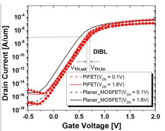
Figure 1.
IDS-VGS characteristics for a VDS of 0.1 [V] and 1.6 [V], and the definition of DIBL. The red symbol shows the measured drain current of the fabricated PiFET structure with 0.1 μm DRAM technology.
The threshold voltage is estimated based on the constant current (10−7 A/μm) method. The VTH in the PiFET, according to VDS, is higher than that in the planar MOSFET, meaning the PiFET has the better DIBL characteristics. We also found that the PiFET has a lower off-current than that in the planar MOSFET when the VGS = 0 V or less.
3. Results and Discussion
3.1. Five Slope
The thickness of the buried insulator of an SOI MOSFET is limited for improved electrical properties, but the buried insulator thickness of the PiFET can be easily controlled for better electrical properties [8,9]. As shown in Figure 2, buried insulator types for PiFET were divided into five slopes, in order to investigate the electrical characteristics according to the lateral encroachment levels in the channel direction. The lateral encroachment of the buried insulator of slope 5 is shorter in the group than in the other slopes. Figure 3 shows the DIBL and the threshold voltage according to the PiFET structures having various types of slopes compared to the planar MOSFET, and the SOI MOSFET at VGS = 0 V and VDS = 1.6 V. The PiFET having slope 5 exhibits better DIBL and a higher threshold voltage than the conventional MOSFETs and the PiFETs, which have gentle slopes 1–4, since the electric field near the source region is smaller. These results are also consistent with those of the planar MOSFETs and SOI MOSFETs. The smaller electric field is formed near the source region in the PiFET having slope 5, mainly because most of the electric field between the drain and the source condenses into the buried insulator, at the bottom of the drain region. This potential condensation phenomenon causes a large threshold voltage, even under low drain voltage conditions. Thus, to maintain a high VTH and DIBL, we found that the buried insulator penetrating into the drain region should be minimized below the channel region. Also, the off-currents, according to slope type of the PiFET, remained almost constant, because the electric field near the overlapped region of the gate and the drain region remains almost constant regardless of the slope type.
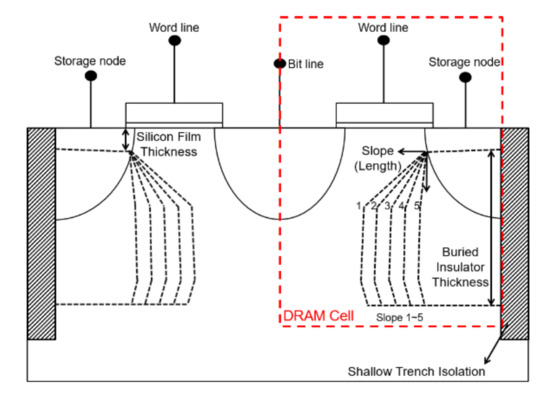
Figure 2.
Several types of PiFET structures, according to the silicon film thickness and the slope.
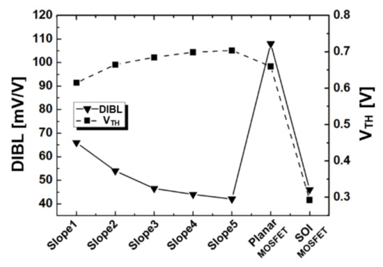
Figure 3.
Simulation results for DIBL and threshold voltage for the planar MOSFET, the SOI MOSFET, and PiFETs with a silicon film thickness of 15 nm and the buried insulators (slopes 1–5) of the SiO2 material.
3.2. Various Dielectric Constants
Figure 4 shows the simulation results of the potential contour near the drain region for the PiFETs and the planar MOSFET, when VGS = 0 V and VDS = 1.6 V. The electrical characteristics, according to the dielectric constants of the buried insulator, could be explained by potential condensation and potential modulation phenomenon occurring near the drain region [14]. In the potential contours shown in Figure 4b–d, the potential modulation means that the starting point of the potential drop is shifted from an n− doped region to an n+ doped region, near the drain region. The potential modulation occurs near the drain region because the penetration of the buried insulator induces a potential drop at a high-doped drain region. Namely, since the potential drop in the buried insulator of the PiFETs remains relatively constant, it results in a strong voltage change near the contact above the buried insulator. Therefore, the depletion region is formed, even in the n+ doped region, where it is difficult for the voltage change to occur in the planar MOSFET. As shown in Figure 4b–d, as the dielectric constant increases, a high drain potential edge is also pushed forward and moves toward the n+ drain region, due to an interaction increase of the boundary surface between the silicon and buried insulator. In other words, the high dielectric constant of the buried insulator deepens the potential modulation. It is found that the potential modulation results in an expanding depletion region near the n+ doped region by a high gate-fringing field. Although a high gate fringing field can cause unintended fringing field-induced barrier-lowering (FIBL) effects, reducing the channel-to-drain barrier, it can reduce the electric field across the gate oxide between the gate and drain regions [15,16]. As shown in Figure 5a, the peak of the vertical field of the overlapped region between the drain and gate of the PiFETs decreases, and is shifted from an n− doped region to an n+ doped region, due to the increased gate-fringing field. This means that the band-to-band tunneling (BTBT) in the overlapped region between the gate and the drain is reduced [17,18,19,20]. Therefore, the PiFET structure can effectively reduce the off-current by GIDL. Meanwhile, Figure 5b shows the potential drop of the PiFETs and planar MOSFET at the channel surface by potential modulation. A deep potential modulation phenomenon in the drain region can consequently contribute to improving the DIBL characteristics, by effectively blocking the electric field transmitted to the source.
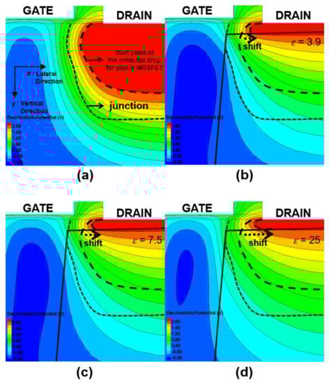
Figure 4.
Two-dimensional potential contour profiles (at VGS = 0.0 V, VDS = 1.6 V) of 0.2 steps near the drain region in (a) planar MOSFET, (b–d) PiFETs with slope 5 and silicon film thickness of 15 nm. (b) k = 3.9, (c) k = 7.5, (d) k = 25.
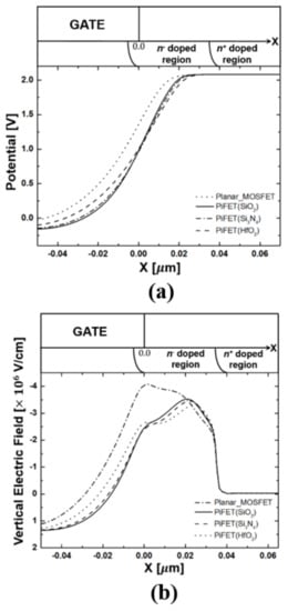
Figure 5.
(a) Vertical electric field distribution and (b) lateral potential distribution on the silicon surface near the drain region for the planar MOSFET and the PiFETs when VGS = − 0.5 V and VDS = 1.6 V.
Figure 6 shows the DIBL and the threshold voltage dependence on the dielectric constant of the buried insulator with slope 5. The PiFET, with a high dielectric constant of 25, has a relatively small electric field inside the buried insulator, thereby reducing the potential drop occurring near the buried insulator formed under the drain. This means that a large electric field penetrates the channel region. That is, as the dielectric constant of the buried insulator with a constant slope increases, the potential condensation phenomenon is weakened. Although the potential modulation phenomenon is strengthened in the PiFET structure of a buried insulator having a higher dielectric constant, the potential condensation phenomenon is the most crucial factor for improving the DIBL in the PiFET structure; it is even more important in PiFET structures with low dielectric constants. Therefore, the PiFET with a high dielectric constant exhibits DIBL and VTH characteristics that are less improved than those of the PiFET having a low dielectric constant; however, the PiFETs exhibit DIBL and a high VTH superior to conventional MOSFETs. Figure 7 shows the drain current in the subthreshold region of the PiFETs and the planar MOSFET. Tunneling of the electrons from gate to drain occurs with difficulty, due to the high gate-fringing field, as shown in Figure 5a. The PiFET having a dielectric constant of 25 exhibits a small drain current compared with the PiFETs with low dielectric constant and planar MOSFET in the region where VGS = 0 V or less. The results in Figure 6 and Figure 7 show that PiFET structures can provide an improved leakage current characterization mechanism for DRAM cell operation. This is because the leakage current characteristics, such as DIBL and GIDL, are likely to be degraded due to the DRAM cell operation when the storage node of the DRAM cell is in a high voltage state.
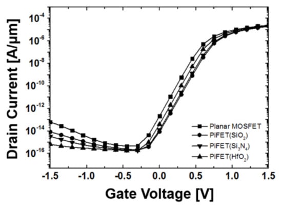
Figure 6.
IDS-VGS indicating off-current characteristics for the planar MOSFET, the PiFET with a silicon film thickness of 15 nm, and the buried insulators of the SiO2, Si3N4, and HfO2 materials.
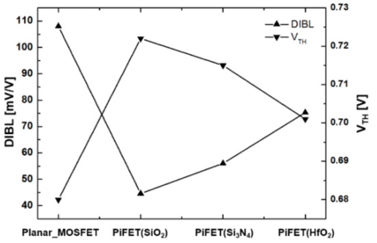
Figure 7.
Simulation results for the DIBL and the threshold voltage for the planar MOSFET and PiFETs with a silicon film thickness of 15 nm and the buried insulators of SiO2, Si3N4, and HfO2 materials.
Figure 8 shows the VDS-IDS characteristics according to the dielectric constant of PiFETs. Even with the high voltage in the drain region, the potential modulation and the potential condensation phenomenon in the PiFET structure minimizes the reduction of the effective channel length. Consequently, the saturation current is kept constant compared to the planar MOSFET, and the PiFET having a low dielectric constant of 3.9 has the most constant saturation current. Figure 9 shows the DIBL characteristics, according to the gate channel lengths of PiFET, SOI MOSFET, and the planar MOSFET. As the gate channel length is reduced, the planar MOSFET and the PiFET with a dielectric constant of 25 show a dramatically increased slope with increasing DIBL, while the PiFET with a dielectric constant of 3.9 maintains a DIBL of less than 150.
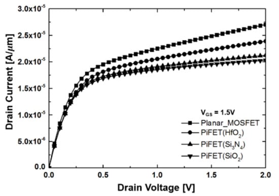
Figure 8.
IDS-VDS characteristics for the planar MOSFET; the PiFET with a silicon film thickness of 15 nm; and the buried insulators of the SiO2, Si3N4, and HfO2 material.
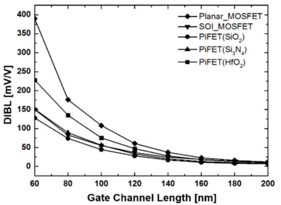
Figure 9.
Simulation results of the DIBL characteristic of planar MOSFET, SOI MOSFET, and PiFETs, each with a silicon film thickness of 15 nm, as well as the buried insulators of the SiO2, Si3N4, and HfO2 materials.
3.3. Silicon Film Thickness
Figure 10 shows the DIBL and VTH characteristics for the PiFET, having a buried insulator of slope 5 with a dielectric constant of 3.9, according to the silicon film thickness. While the SOI MOSFET exhibits improved DIBL characteristics, the threshold voltage is drastically reduced due to the thinner silicon film thickness, which reduces the fully depleted channel region area. However, the PiFET with a thin silicon film exhibits improved characteristics in both the DIBL and the threshold voltage without a fully depleting channel region as the silicon film thickness is reduced. As shown in Figure 11a,b, these improved characteristics also occur because the starting point of the potential drop shifts to the deep n+ doped region when the silicon film thickness is 10 nm, compared to when it is 20 nm. These results indicate that the thin silicon film thickness of PiFET can also induce the potential modulation at the n+ doped region immediately above the buried insulator. Therefore, a large potential drop occurs near the drain region, and the peak vertical electric field decreases near the overlapped region between the drain and gate region, resulting from the high gate-fringing field in the case of thin silicon film thickness, as shown in Figure 12a,b. We thus found that it is possible to enhance the potential modulation phenomenon without a buried insulator with a high dielectric constant, by maintaining the thin silicon film thickness. Figure 13 shows the off-current and Gm.max, according to the silicon film thickness of the PiFET. Actually, the on-current of the PiFETs is almost constant, because the PiFET structure is not related to the area of the source region, although a small drain region limited by the silicon film thickness can slightly reduce the on-current. However, as the silicon film thickness decreases, the off-current sharply decreases. We therefore do not need to seriously consider the Gm.max reduction problem.
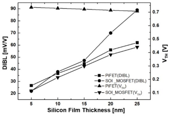
Figure 10.
DIBL and threshold voltage dependence of silicon film thickness on the SOI MOSFET and the PiFET with slope 5.
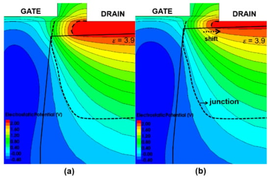
Figure 11.
Two-dimensional potential contour profile (at VGS = 0.0 V, VDS = 1.6 V) of the 0.2 step near the drain region in (a) PiFET (silicon film thickness = 20 nm) and (b) PiFET (silicon film thickness = 10 nm) with slope 5.
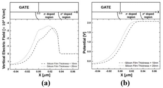
Figure 12.
(a) Vertical electric field distribution and (b) lateral potential distribution on the silicon surface near the drain region for the PiFETs when VGS = − 0.5 V and VDS = 1.6 V.
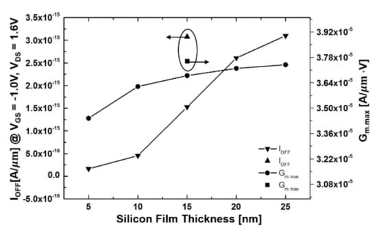
Figure 13.
IOFF and Gm.max dependence of silicon film thickness on the PiFET with slope 5.
4. Conclusions
From the simulation analysis of partial isolation Field-Effect Transistor (PiFET), we found that the potential condensation and potential modulation phenomenon near the drain region caused by the buried insulator considerably improve the DIBL characteristics. In particular, we made the novel discovery that the gate-fringing field effect caused by the potential modulation phenomenon improved the GIDL characteristic by suppressing the BTBT component with a low vertical electric field. Therefore, the PiFET structure is a promising device for improving the properties in the memory cell when designing with precise consideration of the silicon film thicknesses, as well as the shape of the slope of the buried insulator. In addition, the optimized dielectric materials can be chosen as low dielectric constant materials.
Author Contributions
Conceptualization, Y.K.K.; Visualization, J.S.L. and G.K.; Resources, Y.P.C., H.J.K. and Y.J.P; Supervision, T.P. and M.J.L.
Funding
This research was supported in part by the Korea Electric Power Corporation (Grant number: R17XA05-78), in part by the National Research Foundation of Korea (NRF) grant funded by the Korea government (MSIT) (Gant number: 2018R1A2B6008216), in part by the R&D Special Zone Development Project (Technology Transfer Business Project: 17GJI003) funded by the Ministry of Science, and the ICT & INNOPOLIS Foundation.
Conflicts of Interest
The authors declare no conflict of interest.
References
- Chang, L.; Choi, Y.-K.; Ha, D.; Ranade, P.; Xiong, S.; Bokor, J.; Hu, C.; King, T.-J. Extremely scaled silicon nano-CMOS device. Proc. IEEE 2003, 91, 1860–1873. [Google Scholar] [CrossRef]
- Veeraraghavan, S.; Fossum, J.G. Short-Channel Effects in SO1 MOSFET’s. IEEE Trans. Electron Devices 1989, 36, 522–528. [Google Scholar] [CrossRef]
- Risho, K. Buried Layer Engineering to Reduce the Drain-Induced Barrier Lowering of Sub-0.05 µm SOI-MOSFET. Jpn. J. Appl. Phys. 1999, 38, 2294–2299. [Google Scholar]
- Wang, J.; Kistler, N.; Woo, J.; Viswanathan, C.R. Mobility-Field Behavior of Fully Depleted SO1 MOSFET’s. IEEE Electron Device Lett. 1994, 15, 117–119. [Google Scholar] [CrossRef]
- Veeraraghavan, S.; Fossum, J.G. A Physical Short-channel Model for the Thin-Film SOI MOSFET Applicable to Device and Circuit CAD. IEEE Trans. Electron Devices 1988, 35, 1866–1874. [Google Scholar] [CrossRef]
- Koh, R.; Kato, H.; Matsumoto, H. Capacitance Network Model of the Short Channel Effect for 0.1 µm Fully Depleted SOI MOSFET. Jpn. J. Appl. Phys. 1996, 35, 996–1000. [Google Scholar] [CrossRef]
- Kumar, M.J.; Chaudhry, A. Two-Dimensional Analytical Modeling of Fully Depleted DMG SOI MOSFET and Evidence for Diminished SCEs. IEEE Trans. Electron Devices 2004, 51, 569–574. [Google Scholar] [CrossRef]
- Chaudhry, A.; Kumar, M.J. Investigation of the Novel Attributes of a Fully Depleted Dual-Material Gate SOI MOSFET. IEEE Trans. Electron Devices 2004, 51, 1463–1467. [Google Scholar] [CrossRef]
- Joachim, H.O.; Yamaguchi, Y.; Ishikawa, K.; Inoue, Y.; Nishimura, T. Simulation and Two-Dimensional Analytical Modeling of Subthreshold Slope in Ultrathin-Film SOI MOSFET’s Down to 0.1 um Gate Length. IEEE Trans. Electron Devices 1993, 40, 1812–1817. [Google Scholar] [CrossRef]
- Lee, M.J.; Cho, J.H.; Lee, S.D.; Ahn, J.H.; Kim, J.W.; Park, S.W.; Park, Y.J.; Min, H.S. Partial SOI Type Isolation for Improvement of DRAM Cell Transistor Characteristics. IEEE Trans. Electron Devices 2005, 26, 332–334. [Google Scholar]
- Kim, Y.K.; Lee, J.S.; Kim, G.; Park, T.; Kim, H.J.; Cho, Y.P.; Park, Y.J.; Lee, M.J. The optimized Partial Insulator Isolation MOSFET (PiFET). J. Semicond. Technol. Sci. 2017, 17, 729–732. [Google Scholar] [CrossRef]
- Jin, S.; Lee, M.J.; Yi, J.H.; Choi, J.H.; Kang, D.G.; Chung, I.Y.; Park, Y.J.; Min, H.S. New Direct Evaluation Method to Obtain the Data Retention Time Distribution of DRAM. IEEE Trans. Electron Devices 1992, 39, 2244–2350. [Google Scholar] [CrossRef]
- Hurkx, G.A.M.; Klaassen, D.B.M.; Knuvers, M.P.G. A New Recombination Model for Device Simulation Including Tunneling. IEEE Trans. Electron Devices 2006, 53, 331–338. [Google Scholar] [CrossRef]
- Jang, E.; Shin, S.; Jung, J.W.; Kim, K.R. Gate induced drain leakage reduction with analysis of gate fringing field effect on high-κ/metal gate CMOS technology. Jpn. J. Appl. Phys. 2015, 54, 06FG10. [Google Scholar] [CrossRef]
- Cheng, B.; Cao, M.; Rao, R.; Inani, A.; Voorde, P.V.; Greene, W.M.; Stork, J.M.; Yu, Z.; Zeitzoff, P.M.; Woo, J.C. The Impact of High-k Gate Dielectrics and Metal Gate Electrodes on Sub-100 nm MOSFET’s. IEEE Trans. Electron Devices 1999, 46, 1537–1544. [Google Scholar] [CrossRef]
- Ernst, T.; Tinella, C.; Raynaud, C.; Cristoloveanu, S. Fringing fields in sub-0.1 μm fully depleted SOI MOSFETs: Optimization of the device architecture. Solid-State Electron. 2002, 46, 373–378. [Google Scholar] [CrossRef]
- Mizuno, T.; Kobori, T.; Saitoh, Y.; Sawada, S.; Tanaka, T. Gate-Fringing Field Effects on High Performance in High Dielectric LDD Spacer MOSFET’s. IEEE Trans. Electron Devices 1992, 39, 982–989. [Google Scholar] [CrossRef]
- Feng, W.S.; Chan, T.Y.; Hu, C. MOSFET Drain Breakdown Voltage. IEEE Trans. Electron Devices 1986, 7, 572–574. [Google Scholar]
- Chen, J.; Chan, T.Y.; Chen, I.C.; Ko, P.K.; Hu, C. Subbreakdown Drain Leakage Current in MOSFET. IEEE Trans. Electron Devices 1987, 8, 449–450. [Google Scholar] [CrossRef]
- Chen, J.; Assaderaghi, F.; Ko, P.K.; Hu, C. The Enhancement of Gate-Induced-Drain-Leakage (GIDL) Current in Short-Channel SO1 MOSFET and its Application in Measuring Lateral Bipolar Current Gain β. IEEE Trans. Electron Devices 1992, 13, 515–517. [Google Scholar]
© 2018 by the authors. Licensee MDPI, Basel, Switzerland. This article is an open access article distributed under the terms and conditions of the Creative Commons Attribution (CC BY) license (http://creativecommons.org/licenses/by/4.0/).