Article

VCMA-MRAM In-Memory Stochastic Sampling for Edge Boltzmann Machine Inference

1
School of Materials Science and Engineering, Shanghai University, Shanghai 200444, China
2
Institute of Integrated Circuits, Shanghai University, Shanghai 201800, China
3
Nanofabrication Facility, Suzhou Institute of Nano-Tech and Nano-Bionics, Chinese Academy of Sciences, Suzhou 215123, China
*
Authors to whom correspondence should be addressed.
Electronics 2026, 15(8), 1622; https://doi.org/10.3390/electronics15081622
Submission received: 22 March 2026 / Revised: 6 April 2026 / Accepted: 9 April 2026 / Published: 13 April 2026
(This article belongs to the Section Electronic Materials, Devices and Applications)

Abstract

Edge intelligence is often limited by the computation–energy trade-off in resource-constrained devices. Boltzmann machines (BMs) provide strong unsupervised learning capability, yet their reliance on Gibbs sampling makes digital implementations costly in both computation and energy. In this paper, we present a voltage-controlled magnetic anisotropy magnetic tunnel junction (VCMA-MTJ)-based MRAM system that performs in-memory stochastic sampling for state generation and updates in restricted/deep Boltzmann machines (RBMs/DBMs). By exploiting the intrinsic stochastic switching of VCMA-MTJs, the proposed system achieves probabilistic sampling with an energy as low as ∼10 fJ per sample. Implemented on a microcontroller-based edge platform, it enables real-time multi-sensor anomaly detection with an F1-score of 0.9854 and stable operation. The proposed hardware–algorithm co-design achieves in situ stochastic computing and storage within a single MRAM cell, providing an ultra-low-power substrate for probabilistic inference at the edge.

1. Introduction

Restricted Boltzmann Machines (RBMs) and Deep Boltzmann Machines (DBMs) are promising generative models for edge intelligence applications. They offer strong unsupervised learning capabilities and excel in anomaly detection. Specifically, they learn the distribution of normal system states and extract representative features to accurately identify abnormal behaviors [1,2,3]. However, both training and inference typically rely on Markov Chain Monte Carlo (MCMC) methods—especially Gibbs sampling—which require thousands of iterative updates with large-scale matrix–vector operations. This iterative and stochastic sampling process leads to substantial latency, computation cost, and energy consumption, posing a major obstacle to deployment on resource-constrained edge devices. To mitigate this bottleneck, magnetic tunnel junctions (MTJs) have emerged as attractive hardware primitives for energy-efficient implementations, owing to their strengths in probabilistic computing and in-memory computing [4,5,6].
In recent years, magnetic random-access memory (MRAM), a technology platform built upon MTJs, has been considered a potential replacement for conventional embedded Flash (eFlash) and even some SRAM use cases, thanks to its non-volatility, high endurance, fast read/write speed, and low power consumption [7,8,9]. Because Boltzmann machines fundamentally depend on stochastic sampling, MTJs serve as natural hardware enablers: they can generate probabilistic bits via intrinsic stochastic magnetization reversal while providing non-volatile storage through deterministic switching, thereby tightly coupling computation and storage in memory [10]. Exploiting this randomness, MTJs have been applied as stochastic samplers for RBM-based digit recognition [11], combined with FPGAs as p-bits to enable energy-efficient inference and learning in DBMs [12], and used as building blocks of Ising machines for NP-hard problems such as integer factorization [13,14]. Among MTJ variants, voltage-controlled magnetic anisotropy (VCMA) MTJs are particularly appealing for edge applications. Their key advantage is voltage-controlled probabilistic switching, which enables direct and fine-grained tuning of the sampling probability. By applying voltage pulses to modulate the free-layer magnetic anisotropy, VCMA-MTJs can achieve ultra-low energy per sample, higher operating speed, and a compact, scalable cell structure compared with other MTJ counterparts [15].
Despite these significant advantages, achieving accurate probabilistic bit (p-bit) behavior in VCMA-MTJs requires precise pulse generation. Delays and variations in pulse timing due to spatial differences across the MRAM array, coupled with intrinsic device-to-device variability, can lead to systematic sampling errors and severely degrade system performance. To overcome these practical hardware non-idealities and unlock the potential of probabilistic computing at the edge, this work proposes a complete VCMA-MTJ-based in-memory computing system with a hardware–algorithm co-design methodology. By leveraging the intrinsic true-random stochastic switching and non-volatility of VCMA-MTJs, our approach tightly couples computation and storage. This synchronous paradigm inherently supports the Gibbs sampling required by RBMs/DBMs, while eliminating the severe static energy leakage associated with asynchronous sampling and bypassing the latency bottlenecks of traditional von Neumann architectures. Furthermore, to ensure reliable physical operation, we incorporate an on-chip configurable pulse generator and apply a clustering-based calibration methodology to suppress variation-induced errors.
The main contributions of this paper are explicitly summarized as follows:
  • MRAM Design & Energy Efficiency: We design a 192 Kbit VCMA-MTJ-based MRAM macro featuring a synchronous, configurable pulse voltage scheme. By avoiding the continuous static leakage of asynchronous architectures, the proposed memory achieves ultra-low-power probabilistic sampling. It operates with an intrinsic cell energy of ∼10 fJ and a quantified macro-level energy of ∼30.8 pJ per update. This delivers a 1 to 2 orders of magnitude energy reduction compared to both pure software PRNG implementations and asynchronous hardware baselines.
  • Architecture & Circuit Design: We propose a hardware–algorithm co-designed architecture tailored for generative probabilistic models on edge devices. By integrating an on-chip configurable pulse generator, the system performs highly accurate, voltage-controlled in-memory stochastic sampling. This inherently retains model states in non-volatile memory and entirely eliminates the extensive data movement and Boolean logic computation costs required by traditional digital systems.
  • System-Level Validation & Calibration: We establish an end-to-end hardware prototype integrating an MCU and the fabricated VCMA-MRAM chip to deploy a multi-sensor anomaly detection task. To combat inherent device-to-device variability, we introduce a clustering-based calibration step; ablation control experiments confirm that this method effectively suppresses systematic false alarms, restoring the hardware F1-score to 0.9854 and remarkably outperforming pseudo-random software baselines by leveraging correlation-free physical true-randomness.

2. Background

2.1. Probability-Flipping Characteristics of VCMA-MTJ

Figure 1a shows the schematic structure of the VCMA-MTJ. The magnetization switching of its free layer is modulated by applied voltage pulses through the voltage-controlled magnetic anisotropy effect, enabling probabilistic switching behavior [16,17,18,19]. Figure 1b characterizes the switching probability under applied voltage pulses of varying amplitudes. The switching probability exhibits a sigmoidal dependence on the pulse voltage (Figure 1c). The data are fitted with
y = 1 1 + e ( a x + b ) ,
resulting in a = 7.99 and b = 10.68 , with a fitting error of r = 2.6 × 10 3 .
This voltage-tunable probabilistic switching allows VCMA-MTJs to directly implement the Bernoulli sampling required in Boltzmann machines. Specifically, the conditional probabilities for sampling hidden and visible units are given by
p h j = 1 v = σ b j + i = 1 m v i W i j ,
p v i = 1 h = σ a i + j = 1 n h j W i j ,
where v i and h j denote the states of the ith visible neuron and the jth hidden neuron, respectively; a i and b j are the corresponding biases; W i j is the weight; and σ ( · ) is the sigmoid function.
To effectively execute this in hardware, we map the algorithmic activation function directly to the physical device physics. Leveraging the binary nature of the neuron states ( v i , h j { 0 , 1 } ), the MCU simply accumulates the weights corresponding to the active neurons. This resulting sum is linearly scaled and applied via the DAC as the physical programming voltage pulse ( V b ) to the target VCMA-MTJ. Because the device’s intrinsic flipping probability naturally follows a sigmoidal curve (Equation (1)), the MTJ seamlessly acts as a stochastic hardware neuron. Its post-pulse magnetization state directly represents the sampled binary state of the neuron (‘0’ or ‘1’). The physical sampling operation thus directly implements the positive phase p ( h v ) mapping of Equation (2), while the reconstruction phase p ( v h ) of Equation (3) is similarly achieved by adjusting the applied voltage based on the hidden layer states.

2.2. MRAM Structure

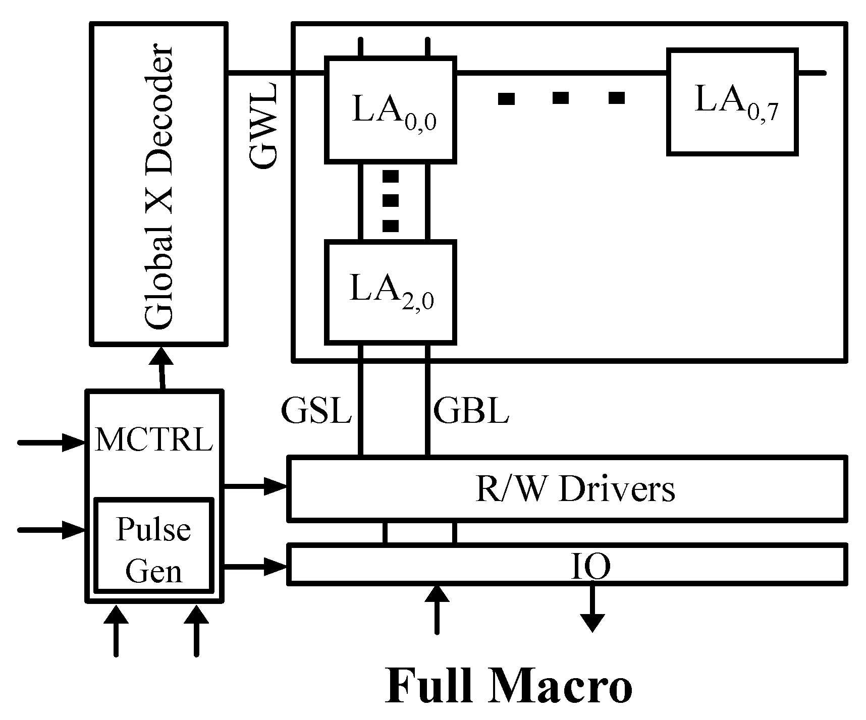
Figure 2 shows the macro organization of the proposed VCMA-MTJ MRAM chip. A total storage capacity of 192 Kbit is implemented by a tiled memory core composed of a 6 × 8 grid of local-array (LA) tiles, where each tile contains a 64 × 64 bitcell array.
At the macro level, the architecture is functionally partitioned into three regions. (1) The global control block (MCTRL) orchestrates command decoding and operation sequencing, and configures the on-chip pulse generator for write/read timing. The pulse generator’s pulse width error is tightly controlled within 0.05 ns, ensuring high precision in timing and minimizing error in write and read operations. (2) The peripheral circuitry integrates the read/write (R/W) drivers and the I/O interface, and delivers the required electrical conditions to the memory core through global distribution networks, including the global wordline control (GWL) and global line networks (GSL/GBL). (3) The core region consists of the LA tile matrix accessed by the global decoder and peripheral drivers.
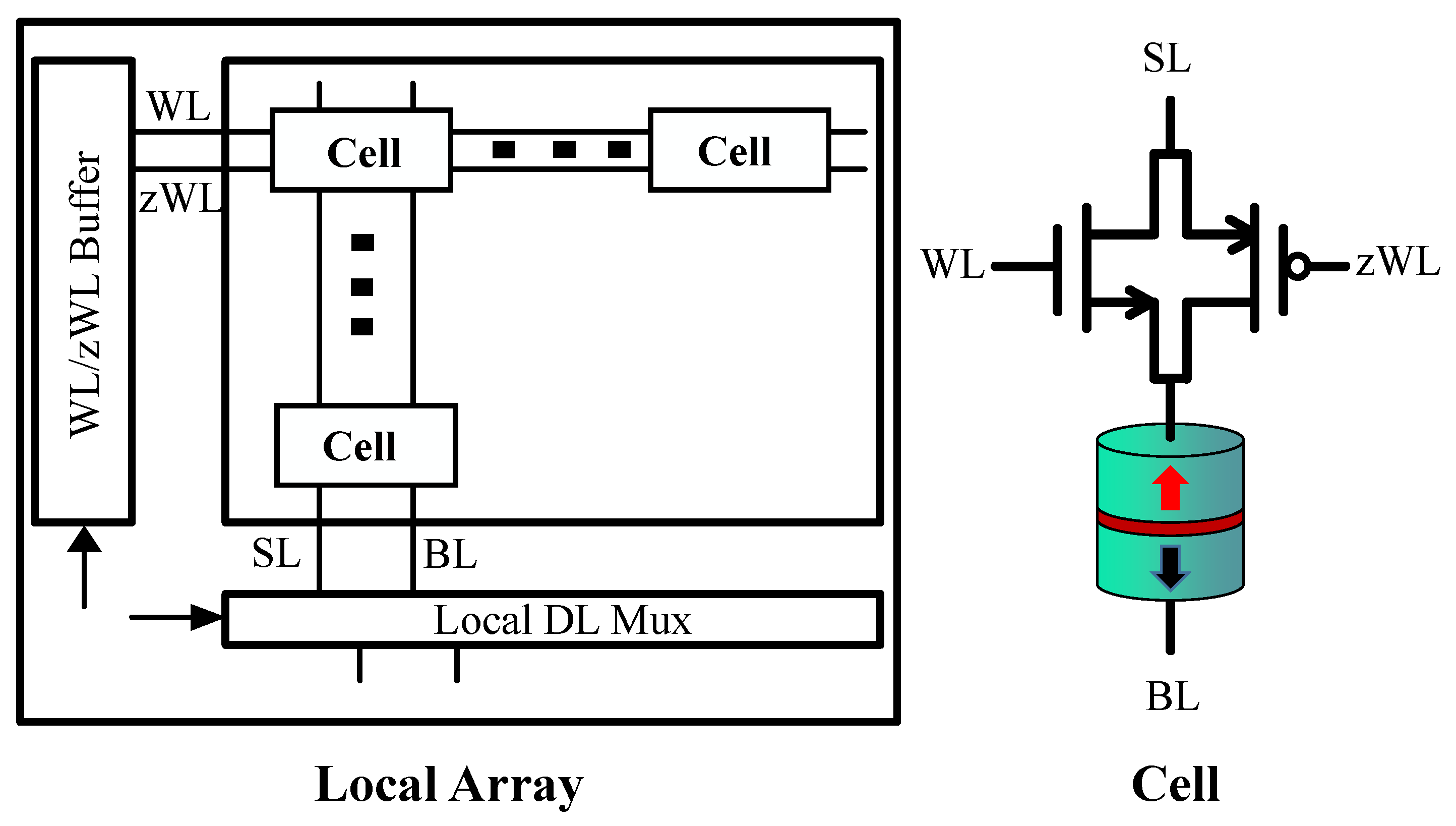
Figure 3 details the structure of an LA tile. In addition to the 64 × 64 cell array, each tile incorporates a local WL/zWL buffer that generates complementary wordline controls for the access devices, as well as a local data-line multiplexer (Local DL Mux) that interfaces the selected column(s) to the peripheral R/W drivers. These local circuits enable scalable tiling by limiting high-capacitance global routing to tile boundaries, while performing final selection and signal conditioning locally.
Each bitcell adopts a two-transistor–one-MTJ (2T1M) topology, as illustrated in Figure 3 (right). The MTJ top electrode is connected to the source line (SL) to receive VCMA write pulses, while the bottom electrode is coupled to the bitline (BL) through a transmission-gate access device controlled by WL and its complement (zWL). During an access, WL/zWL activates the transmission gate to connect the selected MTJ to the column line; the write/read signals are then delivered via the tile interface (through the local multiplexer and the global line networks), without requiring a fixed one-to-one assumption between global and local line naming. In typical operation, the global decoder selects a target tile/row, while the local multiplexer selects the target column(s), enabling distributed addressing with reduced global interconnect capacitance.

3. System Architecture and Network Deployment

3.1. System Design Overview

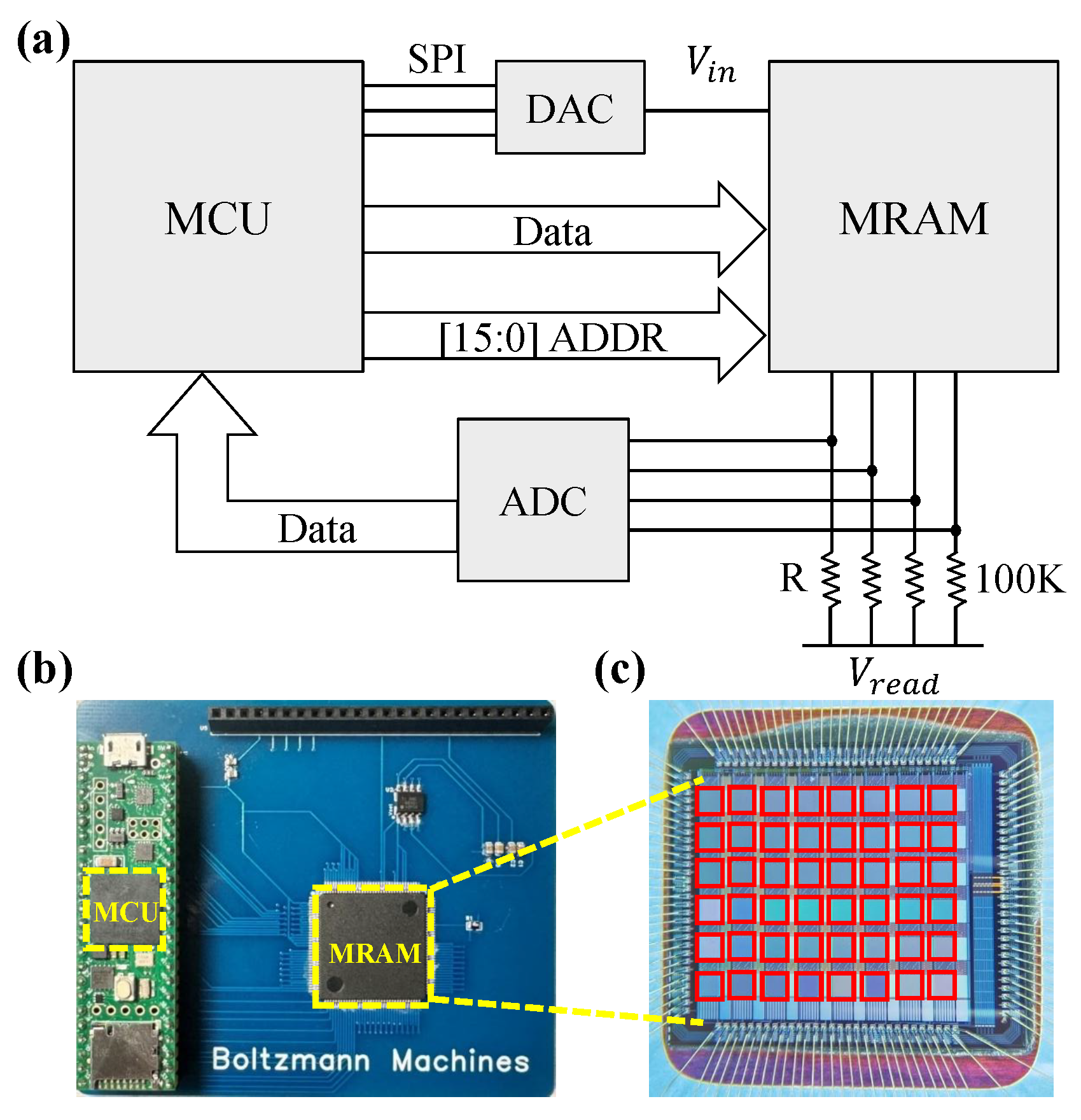
To emulate an MRAM-based embedded control system, we adopt the architecture shown in Figure 4a. The MCU interfaces with the MRAM chip through data and address buses and provides a tunable write voltage via a DAC. Figure 4b,c provides the hardware implementation of the prototype, including the MCU–MRAM test board and the magnified microscope image of the fabricated chip, respectively. To clarify the practical interaction between the MCU and the MRAM during inference, the operational workflow is structured into the following key phases:
  • Configuration Phase (Write Mode): The MCU initializes the system or loads input data. By setting the DAC to a high write voltage (2.4 V), the VCMA-MTJ states are deterministically set to represent the initial visible or hidden layer configurations.
  • Stochastic Sampling Phase (Sampling Mode): During inference, the MCU retrieves the binary states (0 or 1) of the current layer. Leveraging the binary state property, the MCU performs a lightweight accumulation of the relevant weights instead of intensive matrix-vector multiplications. This sum is mapped to a sampling voltage and applied as a 0.49 ns pulse. The VCMA-MTJ then performs the “sampling” operation in-memory via its stochastic switching, effectively generating the next layer’s states.
  • State Retrieval Phase (Read Mode): The updated states of the VCMA-MTJs are sensed via a low-voltage (0.4 V) readout circuit. The comparative result is fed back to the MCU to update the network status or for the next iteration of Gibbs sampling.
As summarized in Table 1, each MRAM address thereby seamlessly transitions between these three core modes to execute the full probabilistic algorithm.

3.2. RBM/DBM Implementation with MRAM

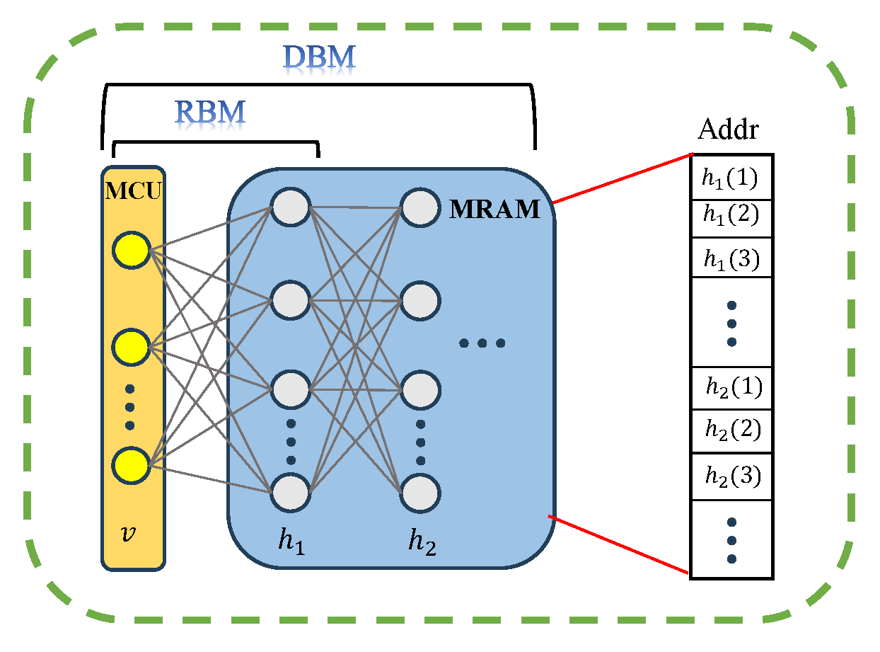
RBMs and DBMs consist of a visible (input) layer and one or more hidden layers. They have no intra-layer connections, while inter-layer connections are fully connected and can be pruned when required. The key distinction is that DBMs include multiple hidden layers, enabling the representation of more complex patterns. As illustrated in Figure 5, the input data acquired by the MCU are mapped to the visible layer, which drives the first hidden layer implemented by the VCMA-MRAM array to perform in-memory sampling. Each MTJ is addressed as a neuron and performs stochastic sampling according to its sigmoidal voltage–probability characteristic; the sampled states are naturally stored as MTJ magnetization states. This sampling can be executed in parallel across multiple addresses, where each address Addr [ i ] ( i = 0 , 1 , 2 , ) corresponds to one MTJ device (i.e., one hidden-layer neuron). During training, visible-layer samples can also be stored in MRAM to support reconstruction. Consequently, the RBM/DBM operation requires the MCU to sequentially read sampled states from the address space of the current hidden layer and to issue sampling commands to the addresses associated with the next layer. While this prototype evaluates an RBM, the RBM serves as the core functional unit of a DBM. Since the layer-wise stochastic sampling process is physically identical, the current hardware validation effectively demonstrates the platform’s scalability to deeper Boltzmann architectures.

3.3. Clustering Analysis for Performance Optimization

For low WER and accurate P-bit behavior in VCMA-MTJs, precise pulse generation is critical. However, pulse delays and variations, caused by spatial differences across the MRAM array and device-to-device variability, can lead to errors in sampling, affecting system performance. Existing variation-aware techniques, such as iterative write-and-verify loops or global voltage guardbanding, often incur severe latency and energy overheads during runtime operation. To address this without compromising efficiency, we applied an offline clustering approach based on the measured sigmoid voltage-probability characteristics of the devices.
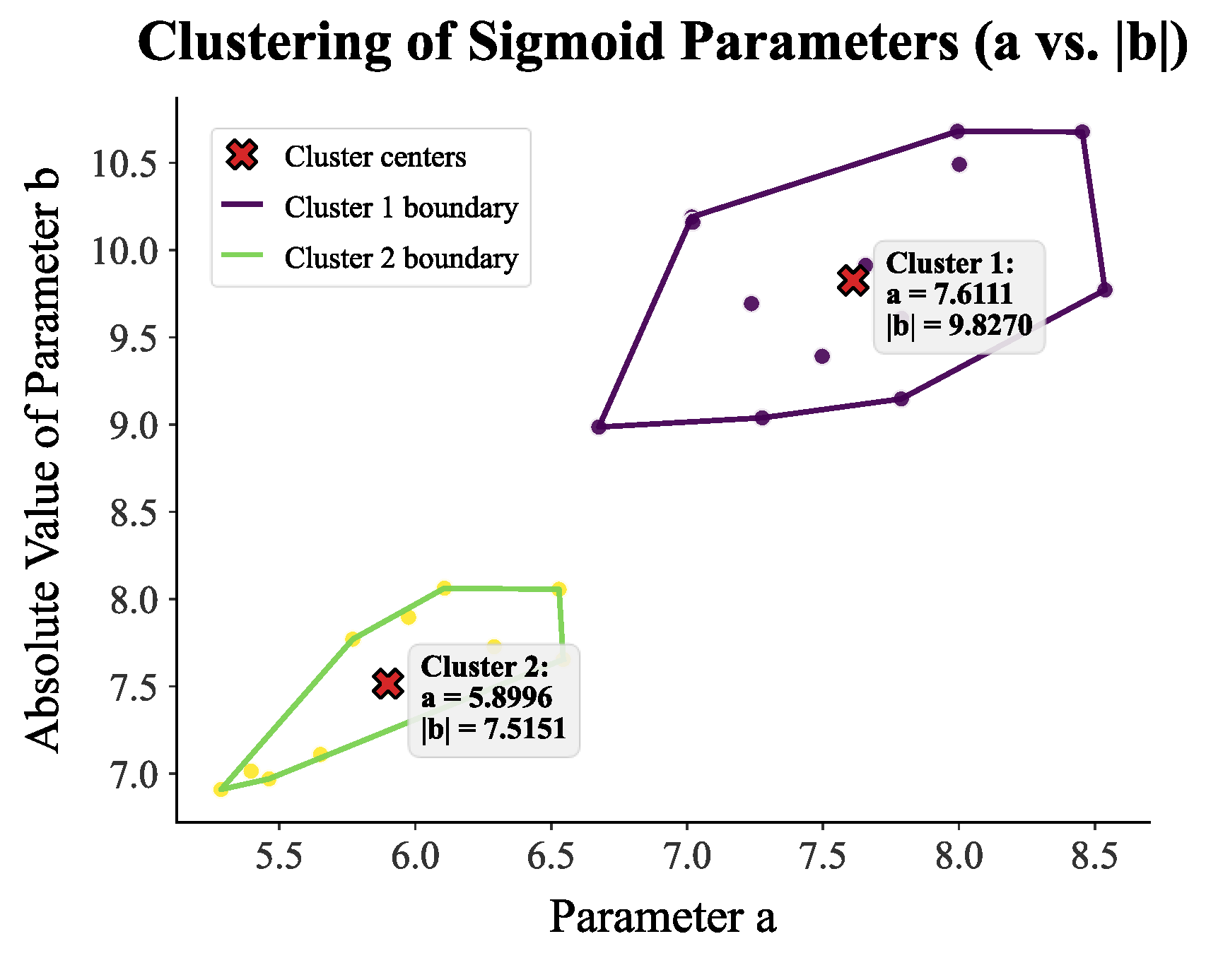
Grouping elements based on their inherent physical or spectral similarities to combat noise and variation is a proven strategy in complex robust systems. For instance, advanced clustering techniques like Enhanced Affinity Propagation Clustering (EAPC) have been successfully utilized to group data based on inherent characteristics, mitigating variability and improving classification in noisy hyperspectral imaging systems [20]. Inspired by this fundamental principle, devices in our array are grouped according to their intrinsic control parameters, such as ( a , | b | ) , which describe their specific sigmoid curve behavior (Figure 6).
Because this calibration is performed as a one-time offline step during system initialization, it assigns optimized baseline control parameters tailored to each specific group without adding any latency or computational overhead to the subsequent hardware training and inference phases. This clustering method effectively reduces errors from device-to-device variability. By dynamically adjusting control parameters based on clustered device characteristics, it enhances the overall reliability and efficiency of the MRAM-based system, maintaining high performance under variability constraints.

4. Results and Discussions

4.1. Experimental Setup and Software Baseline

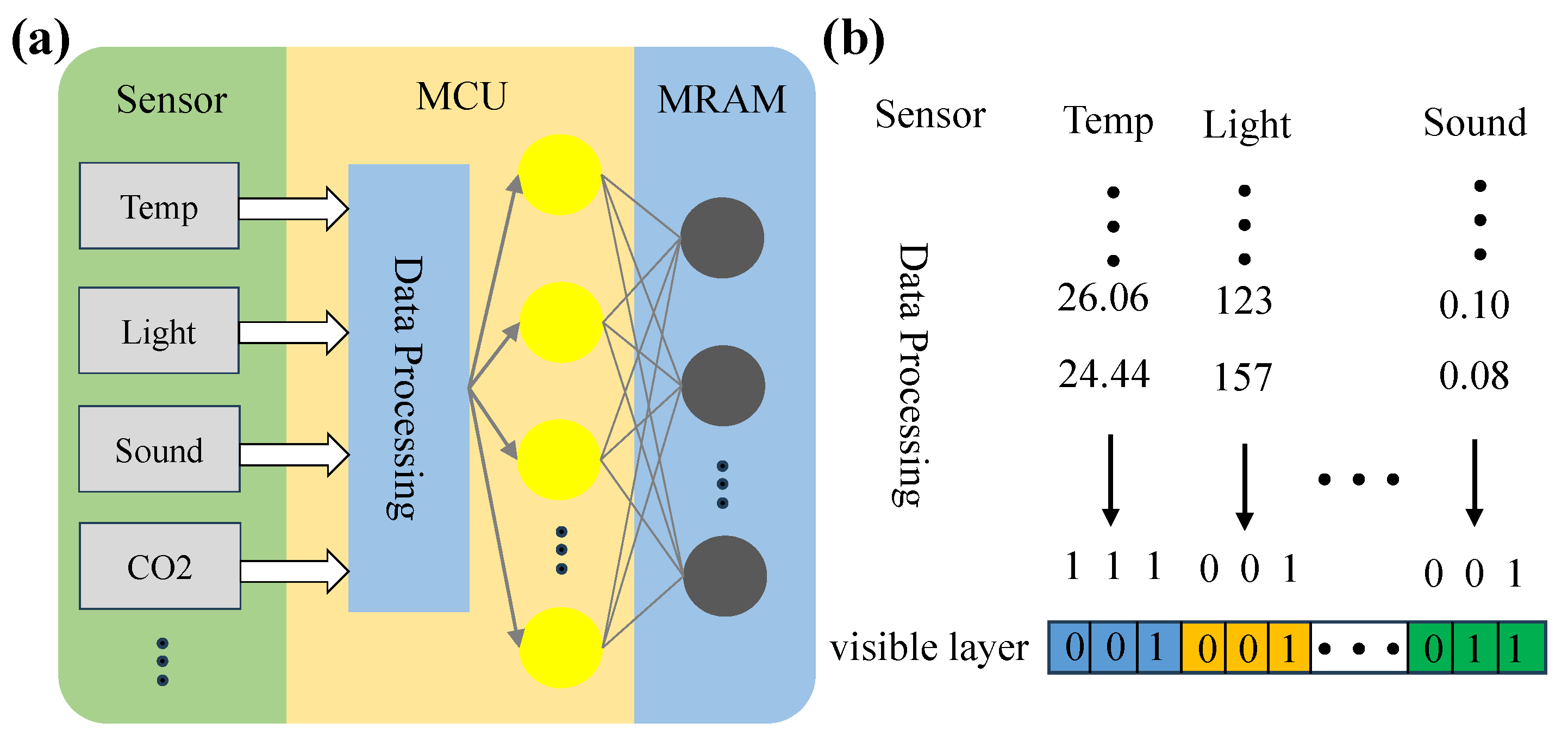
After electrical characterization and parameter group calibration of the VCMA-MTJs, we deployed an RBM onto the MRAM-based hardware platform to enable real-time sensor processing and room occupancy anomaly detection. The system ingests multi-dimensional environmental sensor streams and performs online inference to discriminate occupancy states (“occupied” vs. “unoccupied”) (Figure 7a). Experiments use the public Room Occupancy Estimation dataset [21], which provides temperature, humidity, light, and CO2 measurements, among others, and is suitable for occupancy recognition.
To match the binary neurons in Boltzmann machines, continuous sensor values are discretized using a threshold-based encoding. Three thresholds (10%, 45%, and 80%) map each sensor reading to a 3-bit code, converting 16 sensor channels into a 48-dimensional binary input vector (Figure 7b). This representation is naturally compatible with MRAM’s binary storage. The hidden layer contains 24 units to match the characterized MTJ array. The processing pipeline is: sensor acquisition, binarization, RBM reconstruction, reconstruction-error evaluation, and occupancy decision based on whether the error exceeds a preset threshold; the inferred state then triggers the MCU to execute the corresponding scenario mode.
To benchmark the RBM under hardware-realistic stochastic sampling, we first established an ideal software baseline by executing the RBM training and inference on a standard host PC. The software model was configured with 24 hidden units. The model was trained using the Contrastive Divergence (CD-1) algorithm with a learning rate of 0.01 for 60 iterations. Furthermore, because hidden-layer sampling introduces randomness, we repeated inference 200 times on the test set to analyze the distribution (mean and standard deviation) of the evaluation metrics. As summarized in Table 2, stochastic sampling does not noticeably reduce stability; the standard deviation of the F1-score is 0.0017 across repeated runs. This consistency indicates that the RBM inference is robust to sampling-induced variations.

4.2. On-Hardware Results

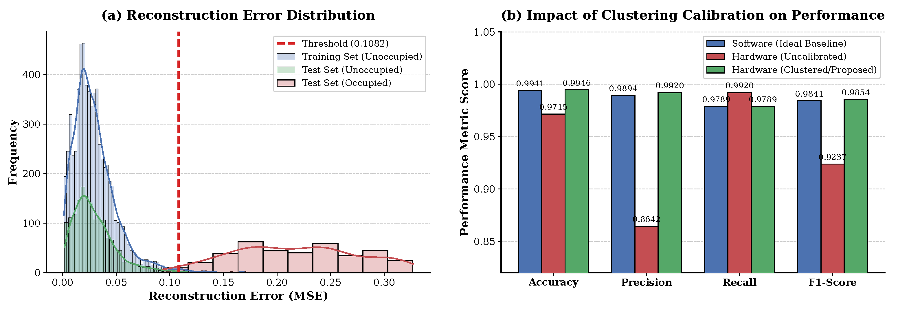
To evaluate the practical viability of our proposed architecture, we execute full RBM training and inference directly on the hardware platform. During the inference phase, the MCU sequentially fetches test samples from the MRAM array to serve as visible-layer inputs. It then orchestrates the Gibbs sampling updates for the hidden layer by leveraging the intrinsic stochasticity of the VCMA-MTJ array. Once the in-memory sampling is complete, the MCU calculates the reconstruction error (Mean Squared Error, MSE) for each sample. As illustrated in Figure 8a, anomaly detection is governed by a dynamic threshold, which is empirically set to 98% of the maximum reconstruction error observed during the training phase. Consequently, test samples yielding an MSE below this threshold are classified as normal (“unoccupied”), whereas those exceeding the threshold are flagged as anomalies (“occupied”). Finally, the MCU aggregates these classification results and transmits the confusion matrix to a host PC for performance evaluation.
A critical challenge in executing reliable probabilistic inference on emerging non-volatile memory arrays is managing the inherent device-to-device variations. To quantitatively substantiate the necessity of our proposed clustering analysis, we conducted an in-depth ablation control experiment directly on the physical MRAM array, as presented in Figure 8b. In an uncalibrated baseline scenario, device variations (previously characterized in Figure 6) are left uncompensated, and a single global average control voltage is uniformly applied to all VCMA-MTJs. Experimental measurements reveal a severe degradation in overall system utility under this naive scheme, with the F1-score dropping to 0.9237. Interestingly, this degradation manifests as a sharp plunge in Precision (0.8642) accompanied by a marginal increase in Recall (0.9920). This counterintuitive phenomenon mathematically reflects the underlying hardware physics: uncompensated device variations act as persistent systematic noise during the Gibbs sampling process. This noise artificially inflates the baseline reconstruction error for all inputs. As a result, the uncalibrated system becomes overly sensitive. It falsely flags many normal states as anomalies (causing a plummeted Precision), even though it misses almost no true anomalies (maintaining a high Recall).
To mitigate these hardware-induced false alarms, we apply the proposed clustering-based calibration methodology. By grouping devices according to their measured physical characteristics and assigning tailored baseline control parameters to each cluster, variation-induced systematic sampling errors are effectively suppressed. As shown in Figure 8b, the calibrated hardware system successfully restores the Precision to 0.9920 and achieves an impressive overall F1-score of 0.9854. Remarkably, this physical hardware performance slightly outperforms the ideal software baseline (Accuracy: 0.9941, Precision: 0.9894, Recall: 0.9789, F1-score: 0.9841). This physically profound result can be attributed to the fundamental difference in entropy sources: while software algorithms rely on pseudo-random number generators (PRNGs) that suffer from hidden periodicities and temporal correlations, our hardware utilizes the true-random thermal noise of VCMA-MTJs. This correlation-free, high-quality physical stochasticity enables more effective state-space exploration during Gibbs sampling, allowing the hardware network to escape local minima and yield superior generative inference. Ultimately, this validates that strategically calibrated spintronic arrays not only match but can actively enhance probabilistic machine learning workloads.

4.3. Energy Consumption Analysis

Evaluating energy efficiency is critical for resource-constrained edge intelligence systems. To provide a rigorous assessment of our proposed paradigm, it is necessary to distinguish the intrinsic memory-compute macro energy from the off-chip prototype overhead (e.g., the discrete MCU, DAC, and PCB traces). The latter are artifacts of the current discrete test vehicle and would be eliminated in a fully integrated System-on-Chip (SoC). In such a custom implementation, the generic external DAC would be replaced by an ultra-low-power, low-resolution embedded DAC co-designed with the pulse generator. Therefore, our analysis focuses on the core array and macro-level consumption, where the 5.1 pJ allocated to the pulse generator explicitly accounts for this optimized on-chip digital-to-analog conversion overhead.
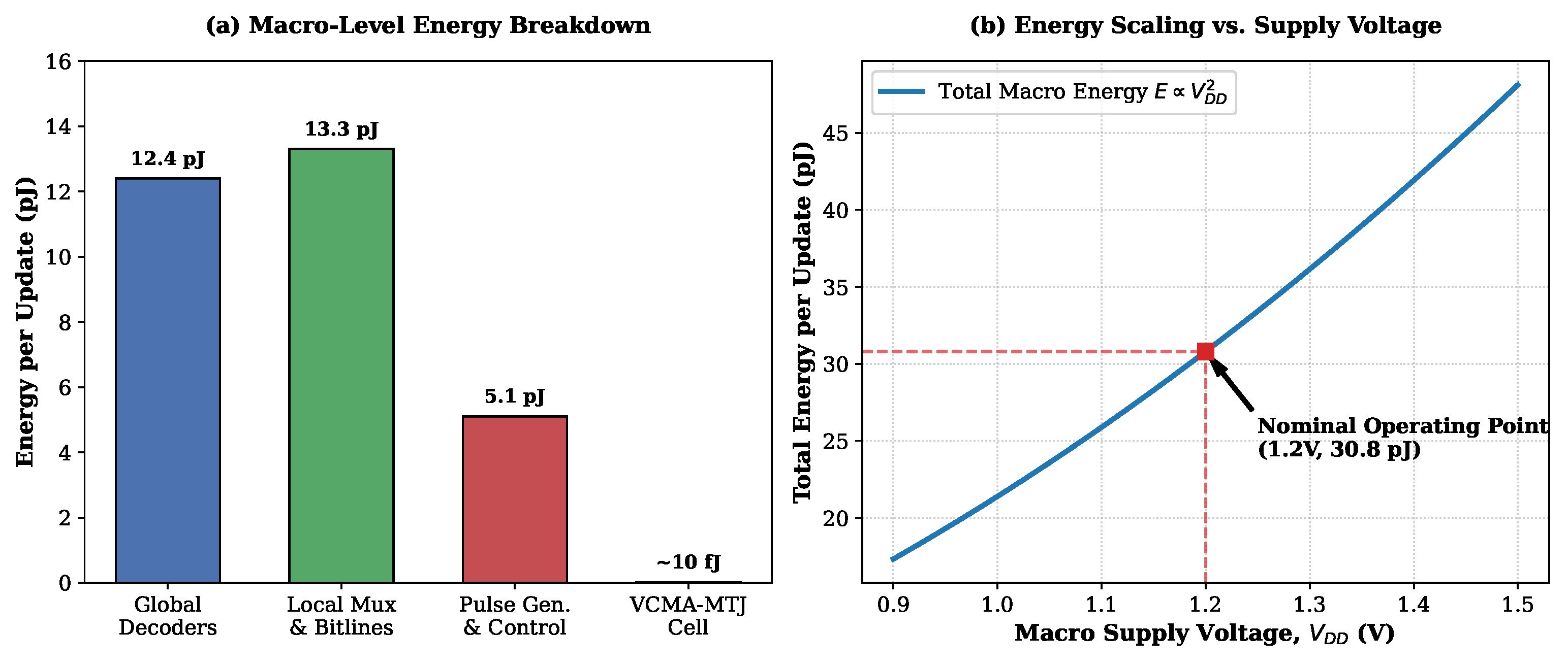
To accurately quantify the macro-level efficiency, we performed a comprehensive circuit-level power breakdown. At the device level, the intrinsic sampling energy is dominated by the sub-nanosecond voltage pulse applied to the VCMA-MTJ cell, which is exceptionally low and calculated at ∼10 fJ per sample. When scaling up to the full MRAM macro, the dynamic power of on-chip peripheral circuits must be accounted for. As illustrated in Figure 9a, the energy breakdown reveals that the global decoders, local data-line multiplexers, and the configurable pulse generator consume 12.4 pJ, 13.3 pJ, and 5.1 pJ, respectively. Consequently, the total energy consumption is analytically derived to be 30.8 pJ per stochastic update at a nominal core voltage of 1.2 V. Furthermore, as governed by the dynamic energy scaling law ( E V D D 2 ) shown in Figure 9b, this macro-level energy is highly dependent on the supply voltage, offering further optimization headroom in advanced technology nodes.
To further contextualize this efficiency, we establish a pure software baseline running on general-purpose edge microcontrollers. Implementing the equivalent Gibbs sampling in software requires executing multi-cycle pseudo-random number generators (PRNGs) and activation functions. Based on official datasheets for modern ultra-low-power edge MCUs, dynamic power consumption typically ranges from ∼3 μA/MHz (e.g., Ambiq Apollo4) to ∼35 μA/MHz (e.g., STM32L4) [22,23,24]. At a nominal core voltage of 1.2 V, this fundamental physical cost translates to 3.6 pJ to 42 pJ per clock cycle. Because a software-based PRNG and thresholding operation demands tens to hundreds of instruction cycles, the energy required for a single sampling update inevitably exceeds 10 3 pJ. Beyond energy efficiency, this hardware–algorithm co-design offers significant advantages in system latency and throughput. In this architecture, the MCU does not participate in the single-bit sampling process; the stochastic generation is an intrinsic physical event. Operating at an experimental system clock of 100 MHz with a 32-bit memory interface, the platform achieves an MRAM read/write throughput of 3.2 Gbps.
This massive algorithmic overhead is explicitly corroborated by recent retrospective benchmarking [13], which quantified the system-level energy cost of a classic hybrid probabilistic computer (relying on an MCU for synaptic routing alongside asynchronous stochastic MTJs [4]) at 1027 pJ per update. Furthermore, FPGA-assisted asynchronous architectures exhibit even higher dissipation (1691 pJ) due to continuous static leakage [12]. To comprehensively evaluate our approach, Table 3 summarizes the energy consumption across various state-of-the-art probabilistic sampling platforms. As demonstrated, our synchronous VCMA-MTJ macro (∼30.8 pJ) is highly competitive with the latest synchronous ASIC implementations based on VCMA-MTJs (34.4 pJ [13]). Crucially, while the design in [13] is restricted to generating fixed 50% probability outputs, our architecture achieves a lower energy footprint while fully supporting the tunable stochasticity required for Boltzmann machine inference. More explicitly, compared to hybrid probabilistic computers relying on MCUs (1027 pJ [4]) and FPGA-assisted asynchronous MTJ architectures (1691 pJ [12]), our proposed design achieves a massive energy reduction of approximately 33 × and 54 × , respectively. It also successfully mitigates the large logic area overhead required by purely digital true-random chaotic oscillators [25]. Ultimately, by replacing power-hungry Boolean logic with intrinsic physical stochasticity within a synchronous array, our hardware–algorithm co-design provides a highly explicit efficiency gain, delivering a 1 to 2 orders of magnitude energy reduction compared to both pure software execution and asynchronous hardware baselines.

5. Conclusions

In this work, we presented a hardware–algorithm co-design paradigm leveraging voltage-controlled magnetic tunnel junctions (VCMA-MTJs) as intrinsic entropy sources for highly efficient probabilistic computing. To overcome the inherent device-to-device variations that typically plague emerging non-volatile memories, we introduced a clustering-based calibration methodology. Our physical control experiments demonstrated that uncompensated hardware variations act as systematic noise, artificially inflating reconstruction errors and severely degrading system precision. However, by grouping devices according to their physical characteristics and assigning tailored control parameters, our calibrated hardware effectively suppressed these variation-induced false alarms. The proposed calibration successfully restored the system’s F1-score to 0.9854, tightly aligning the physical hardware performance with the ideal software baseline.
Furthermore, we comprehensively quantified the energy efficiency of the proposed synchronous MRAM macro. By replacing power-hungry Boolean logic and eliminating the massive static leakage of asynchronous physical sampling, the proposed architecture reduces the macro-level energy to approximately 30.8 pJ per stochastic update. This architecture achieves an energy reduction of 1 to 2 orders of magnitude compared to both pure software PRNG implementations and asynchronous hardware baselines. Ultimately, this work validates that strategically calibrating and integrating VCMA-MTJ arrays can unlock highly efficient, variation-tolerant in-memory Gibbs sampling, paving the way for advanced energy-based machine learning on resource-constrained edge devices.

Author Contributions

Conceptualization, X.D.; methodology, X.D.; software, X.D.; validation, X.D., Y.L. and B.F.; formal analysis, X.D., B.F. and L.W.; investigation, X.D. and B.F.; resources, Y.L., B.F. and L.W.; data curation, X.D.; writing—original draft preparation, X.D.; writing—review and editing, B.F. and L.W.; visualization, X.D.; supervision, B.F. and L.W.; project administration, B.F. and L.W. All authors have read and agreed to the published version of the manuscript.

Funding

The work was supported by Frontier Technologies R&D Program of Jiangsu (No. BF2025031) and the National Natural Science Foundation of China (Nos. 52371206, 12474127, and U24A6001). This work was supported in part by CAS Young Talent Program and the Gusu Leading Talents Program (No. ZXL2023172).

Data Availability Statement

The data presented in this study are available in the article.

Conflicts of Interest

The authors declare no conflicts of interest.

References

  1. Aslan, N.; Dogan, S.; Koca, G.O. Automated classification of brain diseases using the Restricted Boltzmann Machine and the Generative Adversarial Network. Eng. Appl. Artif. Intell. 2023, 126, 106794. [Google Scholar] [CrossRef]
  2. Lü, X.; Long, L.; Deng, R.; Meng, R. Image feature extraction based on fuzzy restricted Boltzmann machine. Measurement 2022, 204, 112063. [Google Scholar] [CrossRef]
  3. Luo, X.; Feng, Y. An underwater acoustic target recognition method based on restricted Boltzmann machine. Sensors 2020, 20, 5399. [Google Scholar] [CrossRef] [PubMed]
  4. Borders, W.A.; Pervaiz, A.Z.; Fukami, S.; Camsari, K.Y.; Ohno, H.; Datta, S. Integer factorization using stochastic magnetic tunnel junctions. Nature 2019, 573, 390–393. [Google Scholar] [CrossRef] [PubMed]
  5. Jung, S.; Lee, H.; Myung, S.; Kim, H.; Yoon, S.K.; Kwon, S.W.; Ju, Y.; Kim, M.; Yi, W.; Han, S.; et al. A crossbar array of magnetoresistive memory devices for in-memory computing. Nature 2022, 601, 211–216. [Google Scholar] [CrossRef] [PubMed]
  6. Zhang, R.; Li, X.; Wan, C.; Hoffmann, R.; Hindenberg, M.; Xu, Y.; Liu, S.; Kong, D.; Xiong, S.; He, S.; et al. Probabilistic greedy algorithm solver using magnetic tunneling junctions for traveling salesman problem. Nat. Commun. 2025, 17, 189. [Google Scholar] [CrossRef] [PubMed]
  7. Wang, C.; Wang, Z.; Li, S.; Zhang, Z.; Zhang, Y. Variation aware evaluation approach and design methodology for SOT-MRAM. IEEE Trans. Circuits Syst. I Regul. Pap. 2024, 71, 1651–1664. [Google Scholar] [CrossRef]
  8. Verma, G.; Soni, S.; Nisar, A.; Kaushik, B.K. Multi-bit MRAM based high performance neuromorphic accelerator for image classification. Neuromorphic Comput. Eng. 2024, 4, 014008. [Google Scholar] [CrossRef]
  9. Jahannia, B.; Ghasemi, S.A.; Farbeh, H. An energy efficient multi-retention STT-MRAM memory architecture for IoT applications. IEEE Trans. Circuits Syst. II Express Briefs 2023, 71, 1431–1435. [Google Scholar] [CrossRef]
  10. Yuan, X.; Jian, J.; Chai, Z.; An, S.; Gao, Y.; Zhou, X.; Zhang, J.F.; Zhang, W.; Min, T. Markov Chain Signal Generation Based on Single Magnetic Tunnel Junction. IEEE Electron Device Lett. 2023, 44, 1963–1966. [Google Scholar] [CrossRef]
  11. Li, X.; Wan, C.; Zhang, R.; Zhao, M.; Xiong, S.; Kong, D.; Luo, X.; He, B.; Liu, S.; Xia, J.; et al. Restricted Boltzmann machines implemented by spin–orbit torque magnetic tunnel junctions. Nano Lett. 2024, 24, 5420–5428. [Google Scholar] [CrossRef] [PubMed]
  12. Singh, N.S.; Kobayashi, K.; Cao, Q.; Selcuk, K.; Hu, T.; Niazi, S.; Aadit, N.A.; Kanai, S.; Ohno, H.; Fukami, S.; et al. CMOS plus stochastic nanomagnets enabling heterogeneous computers for probabilistic inference and learning. Nat. Commun. 2024, 15, 2685. [Google Scholar] [CrossRef] [PubMed]
  13. Duffee, C.; Athas, J.; Shao, Y.; Melendez, N.D.; Raimondo, E.; Katine, J.A.; Camsari, K.Y.; Finocchio, G.; Khalili Amiri, P. An integrated-circuit-based probabilistic computer that uses voltage-controlled magnetic tunnel junctions as its entropy source. Nat. Electron. 2025, 8, 784–793. [Google Scholar] [CrossRef]
  14. Huang, W.; Zhang, K.; Wang, J.; Liu, Y.; Zhang, B.; Zhang, Y.; Zhao, W.; Zeng, L.; Zhang, D. A Novel P-bit Unit Based on VGSOT-MTJ for Reconfigurable Ising Machine With Fully Parallel Spin Updating Design. IEEE Electron Device Lett. 2025, 46, 1889–1892. [Google Scholar] [CrossRef]
  15. Shao, Y.; Khalili Amiri, P. Progress and application perspectives of voltage-controlled magnetic tunnel junctions. Adv. Mater. Technol. 2023, 8, 2300676. [Google Scholar] [CrossRef]
  16. Suhail, H.; He, H.; Yang, J.; Shu, Q.; Wang, C.Y.; Yang, S.Y.; Hsin, Y.C.; Shih, C.Y.; Lee, H.H.; Wu, D.; et al. The first CMOS-integrated voltage-controlled MRAM with 0.7 ns switching time. In Proceedings of the 2023 International Electron Devices Meeting (IEDM), San Francisco, CA, USA, 9–13 December 2023; IEEE: New York, NY, USA, 2023; pp. 1–4. [Google Scholar]
  17. Kang, W.; Ran, Y.; Zhang, Y.; Lv, W.; Zhao, W. Modeling and exploration of the voltage-controlled magnetic anisotropy effect for the next-generation low-power and high-speed MRAM applications. IEEE Trans. Nanotechnol. 2017, 16, 387–395. [Google Scholar] [CrossRef]
  18. Alzate, J.G.; Amiri, P.K.; Upadhyaya, P.; Cherepov, S.; Zhu, J.; Lewis, M.; Dorrance, R.; Katine, J.; Langer, J.; Galatsis, K.; et al. Voltage-induced switching of nanoscale magnetic tunnel junctions. In Proceedings of the 2012 International Electron Devices Meeting, San Francisco, CA, USA, 10–13 December 2012; IEEE: New York, NY, USA, 2012; pp. 29.5.1–29.5.4. [Google Scholar]
  19. Ikeda, S.; Miura, K.; Yamamoto, H.; Mizunuma, K.; Gan, H.; Endo, M.; Kanai, S.; Hayakawa, J.; Matsukura, F.; Ohno, H. A perpendicular-anisotropy CoFeB–MgO magnetic tunnel junction. Nat. Mater. 2010, 9, 721–724. [Google Scholar] [CrossRef] [PubMed]
  20. Daniel, V.A.A.; Vijayalakshmi, K.; Pawar, P.P.; Kumar, D.; Bhuvanesh, A.; Christilda, A.J. Enhanced affinity propagation clustering with a modified extreme learning machine for segmentation and classification of hyperspectral imaging. e-Prime Adv. Electr. Eng. Electron. Energy 2024, 9, 100704. [Google Scholar] [CrossRef]
  21. Singh, A.P.; Chaudhari, S. Room Occupancy Estimation; UCI Machine Learning Repository: Irvine, CA, USA, 2018. [Google Scholar] [CrossRef]
  22. Ambiq Micro. Apollo4 Blue Plus SoC Datasheet. 2023. Available online: https://ambiq.com/apollo4-blue-plus/ (accessed on 1 March 2026).
  23. STMicroelectronics. STM32L476xx Ultra-Low-Power Arm Cortex-M4 32-Bit MCU+FPU Datasheet; STMicroelectronics: Geneva, Switzerland, 2021; Rev. 7. [Google Scholar]
  24. Mittal, S. A survey of techniques for approximate computing. ACM Comput. Surv. (CSUR) 2016, 48, 62. [Google Scholar] [CrossRef]
  25. Lee, W.; Kim, H.; Jung, H.; Choi, Y.; Jeon, J.; Kim, C. Correlation free large-scale probabilistic computing using a true-random chaotic oscillator p-bit. Sci. Rep. 2025, 15, 8018. [Google Scholar] [CrossRef] [PubMed]
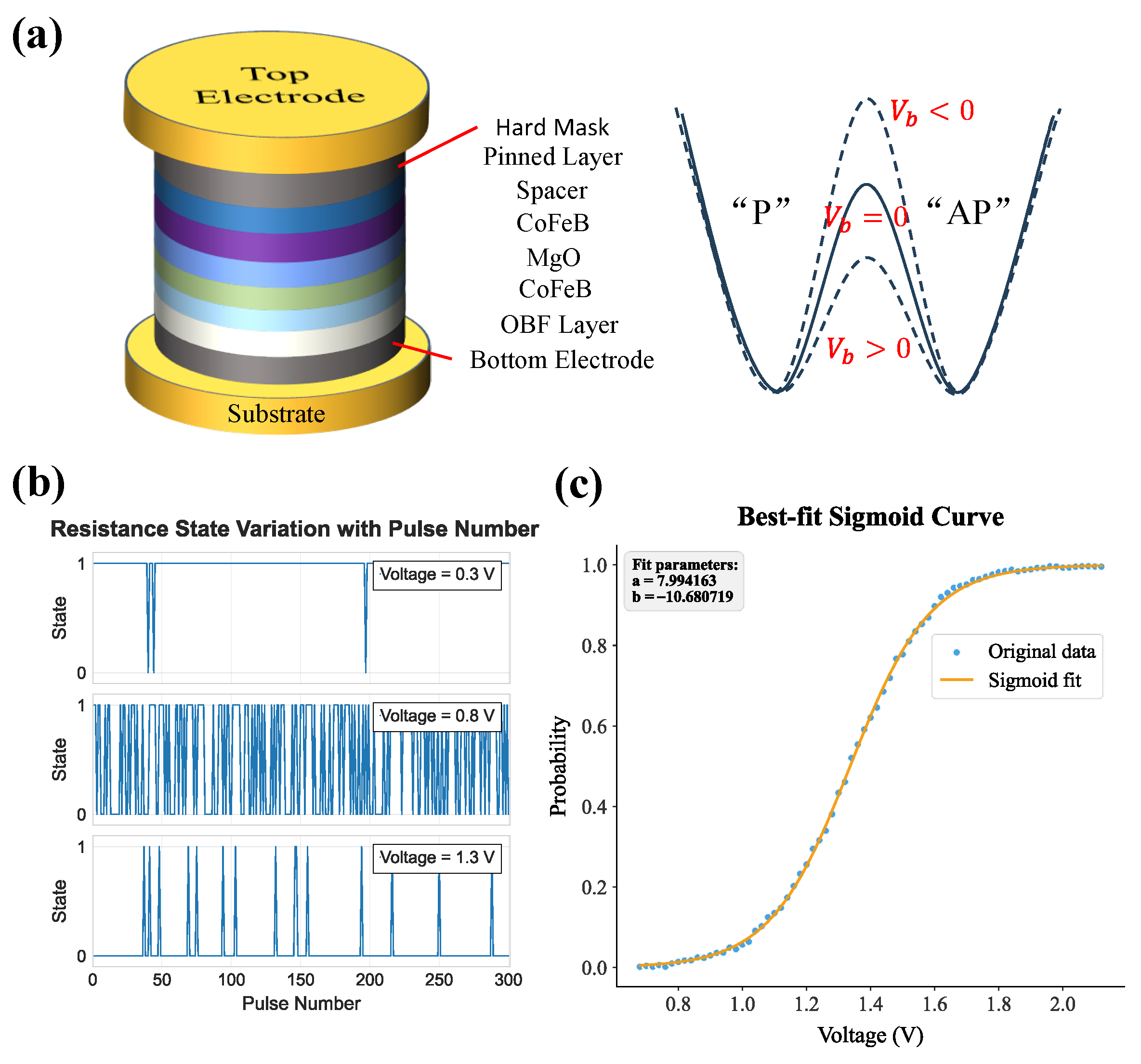
Figure 1. (a) Schematic of the VCMA-MTJ device structure and the energy landscape illustrating voltage-induced stochastic switching. Applying a voltage pulse ( V b ) lowers the energy barrier between the P and AP states. (b) Measured time-domain stochastic switching of the MTJ under 0.5-ns voltage pulses. (c) The switching probability versus voltage is fitted with a sigmoidal function, yielding a = 7.99 and b = 10.68 .
Electronics 15 01622 g001
Figure 2. Top-level macro architecture of the proposed VCMA-MTJ MRAM chip.
Electronics 15 01622 g002
Figure 3. Local-array organization and bitcell schematic. The illustration shows the architecture of a single memory block and the schematic of the 2T1M-based cell used throughout the array.
Electronics 15 01622 g003
Figure 4. (a) System architecture. (b) The entire hardware system is integrated on a single PCB, including MRAM and MCU. (c) The magnified microscope image of MRAM.
Electronics 15 01622 g004
Figure 5. RBM/DBM network schematic, showing full connectivity between visible and hidden layers, with hidden neurons stored in MRAM.
Electronics 15 01622 g005
Figure 6. Cluster analysis separates devices into two groups, G1 (purple dots) and G2 (yellow dots), with centroids at (7.61, 9.83) and (5.90, 7.52), respectively.
Electronics 15 01622 g006
Figure 7. (a) Multi-sensor room occupancy detection platform schematic: MCU-preprocessed multi-sensor data is fed into the RBM, and the MCU calculates reconstruction error between RBM output and input. (b) Data pre-processing flow.
Electronics 15 01622 g007
Figure 8. (a) Distribution of reconstruction errors on the training set and the anomaly decision threshold set at 98% of the maximum error. (b) Comparison of hardware-based and software-simulated performance metrics.
Electronics 15 01622 g008
Figure 9. Circuit-level energy evaluation of the proposed MRAM macro. (a) Energy breakdown of the active on-chip components per stochastic update. (b) Analytical energy scaling curve demonstrating the quadratic dependence on the macro supply voltage ( V D D ), with the nominal operating point marked at 30.8 pJ.
Electronics 15 01622 g009
Table 1. Operation parameters and flipping probability of VCMA-MTJ.
OperationAmplitude (V)Width (ns)Probability of Flipping
Read0.40.490
Write2.40.491
Samplingv0.49 Sigmoid ( v )
Table 2. Distribution of performance metrics.
Evaluation MetricsAverageStandard Deviation
Accuracy0.99400.0006
Precision0.98920.0033
Recall0.97880.0002
F1-score0.98400.0017
Table 3. Energy consumption comparison for probabilistic (Gibbs) sampling.
Reference/YearHardware PlatformEntropy Source & Update MechanismMacro/System EnergyDevice/Cell Energy
Software BaselineGeneral Edge MCUSoftware PRNG + Activation>1000 pJN/A
Borders et al. (2019) [4]MCU + s-MTJStochastic MTJ (Asynchronous)1027 pJ
Singh et al. (2024) [12]FPGA + s-MTJStochastic MTJ (Asynchronous)1691 pJ
Kim et al. (2024) [25]Digital ASICChaotic Oscillator (True-random)4.26 pJ
Duffee et al. (2025) [13]ASIC + V-MTJVCMA-MTJ (Synchronous)34.4 pJ0.43 pJ (430 fJ)
This WorkCustom MRAM MacroVCMA-MTJ (Synchronous)∼30.8 pJ∼0.01 pJ (10 fJ)
Note: N/A and – denote not applicable and data not available in the cited literature, respectively. Macro/System Energy accounts for the generation of random numbers and necessary peripheral support circuits (e.g., decoders, multiplexers, and pulse generators). Device/Cell Energy refers solely to the intrinsic physical switching energy of the entropy source. For Borders et al. (2019), the 1027 pJ system-level energy is derived from the retrospective benchmarking analysis in [13].
Disclaimer/Publisher’s Note: The statements, opinions and data contained in all publications are solely those of the individual author(s) and contributor(s) and not of MDPI and/or the editor(s). MDPI and/or the editor(s) disclaim responsibility for any injury to people or property resulting from any ideas, methods, instructions or products referred to in the content.