
Article

A Simplified Equivalent Circuit Model of a Phase-Shift Series Resonant Converter

Department of Electrical Engineering, Korea National University of Transportation, Chungju 27469, Republic of Korea
*
Author to whom correspondence should be addressed.
Electronics 2026, 15(7), 1491; https://doi.org/10.3390/electronics15071491
Submission received: 13 March 2026 / Revised: 30 March 2026 / Accepted: 31 March 2026 / Published: 2 April 2026

Abstract

The series resonant converter (SRC) is widely used in power conversion systems that require high efficiency and high-power density. However, under light-load conditions, the resonant current decreases, and a higher switching frequency is often required to regulate the output voltage, which leads to efficiency degradation. To mitigate this issue, phase-shift control can be applied to the SRC, and an appropriate small-signal model is essential for accurate dynamic analysis and controller design. Conventional extended describing function (EDF)-based small-signal models provide high accuracy, but their complex equivalent circuits make analytical derivation of the transfer functions difficult and limit intuitive physical interpretation. To overcome this limitation, this paper proposes a non-coupled third-order equivalent-circuit model for the phase-shift SRC. The proposed model reduces the complexity of the conventional EDF-based fifth-order model while preserving the essential low-frequency dynamic characteristics. By employing approximations based on the relationship between the modulation frequency and the switching frequency, together with the superposition principle and equivalent transformations, the model removes the coupling among state variables and enables analytical derivation of the transfer functions. The proposed model is verified through comparisons of the low-frequency small-signal frequency responses with the conventional fifth-order model, PLECS simulations, and experimental measurements.

1. Introduction

Recently, resonant converters have been widely adopted as key power-conversion topologies in applications requiring high efficiency and high-power density, such as electric vehicles (EVs), energy storage systems (ESSs), and renewable-energy interfaced systems [1,2,3,4,5].
Among various resonant-converter topologies, the series resonant converter (SRC) has been widely used due to its simple structure and inherent soft-switching capability. However, in SRC, the resonant-tank current depends on the load current, and thus it decreases as the load is reduced. As a result, under light-load conditions, the resonant-tank current may be insufficient to sustain soft switching. Moreover, as the operation moves toward light-load conditions, a higher switching frequency is often required to regulate the output voltage, which can lead to loss of soft switching, increased switching losses, and degraded overall efficiency [6,7].
To address these issues, this study employs phase-shift control in the SRC so that the output voltage can be regulated under light-load conditions without excessively increasing the switching frequency or incurring additional switching losses [8,9]. For stable output voltage regulation and accurate analysis of the dynamic characteristics of the SRC with phase-shift control, a precise small-signal model is required. To this end, various small-signal modeling approaches capable of accurately capturing beat-frequency dynamics arising from the interaction between the switching frequency and the resonant tank natural frequency have been proposed [10,11,12,13,14,15,16,17,18,19,20]. First, the conventional state-space averaging method exists as one of the representative modeling approaches [10,11,12]. However, this approach is difficult to apply to the small-signal modeling of resonant converters. This is because the state variables produced by the switching network inherently exhibit large-amplitude sinusoidal AC waveforms dominated by harmonic components, so the small-ripple approximation does not hold even when a small DC component is present. In addition, since the average values of these signals approach zero, it is also challenging to derive an averaged model. To address this limitation, small-signal modeling methods based on the extended describing function (EDF) concept have been proposed [13,14,15,16,17]. In EDF, nonlinear variables are approximated by their fundamental components; then, based on harmonic-balance theory, the fast-varying cosine and sine terms are eliminated, and the system is represented in a linear time-invariant form using slowly varying harmonic coefficients. Small-signal models derived using the EDF concept include sine and cosine terms in the state variables, which complicates the model structure and makes it difficult to obtain analytical expressions for the transfer functions. In addition, various modeling approaches such as sampled-data methods, generalized averaging concepts, and methods combining state-space analysis with discrete-time analysis have been presented [18,19,20,21].
These methods can predict the beat-frequency dynamics with reasonable accuracy. However, their relatively involved mathematical formulations limit intuitive physical insight from a circuit perspective. The proposed third-order small-signal equivalent-circuit model exploits the property that the resonant capacitor behaves as an inductor when the modulation frequency is sufficiently lower than the switching frequency and thus analyzes the circuit by replacing the resonant capacitor with an equivalent inductor. In addition, by applying the superposition principle, the coupling terms among state variables are eliminated, and an equivalent non-coupled model is established. This approach reduces the model order, simplifies the transfer-function derivation, and facilitates not only analytical expressions but also physical interpretation of the equivalent circuit.
Various simplified small-signal models have been reported in the literature, including the studies cited above. However, they differ in terms of the target topology, control method, approximation assumptions, and intended application. In particular, ref. [13] provides the conventional EDF-based SRC, while [14] presents a simplified PFM (pulse frequency modulation) SRC equivalent-circuit model. Ref. [14] is the only directly comparable prior work that presents a non-coupled equivalent-circuit model for the SRC, and it is therefore treated as the primary point of comparison in explaining the distinction of the present work. Accordingly, the control input, coefficient definitions, and perturbation-path structure differ from those of [14]. By contrast, the present work focuses on the phase-shift SRC, for which the dominant control path is represented by the phase-shift (duty) perturbation. Related equivalent-circuit modeling studies for resonant topology have also been reported in the literature [15].
The objective of this paper is not to provide a general performance comparison with these simplified models, but rather to address the structural complexity of the conventional EDF-based fifth-order small-signal equivalent-circuit model for the SRC in the phase-shift control case.
To this end, the conventional EDF-based fifth-order model is reduced to third order, and a simplified non-coupled third-order equivalent-circuit model is derived through equivalent-circuit transformation and decoupling procedures while preserving the essential low-frequency dynamics. The proposed model is formulated in a form suitable for controller-oriented low-frequency analysis and enables analytical derivation of the key transfer functions. Unlike the conventional EDF-based fifth-order model, the proposed formulation provides a simpler structure for analytical derivation and circuit-level interpretation. For analytical simplicity, the proposed non-coupled equivalent-circuit model is derived under an ideal-circuit assumption with neglected parasitic and loss elements. In addition, the proposed approach may be extendable to SRCs employing other control methods. However, because the control input and the coupling structure among the state variables may differ, separate reformulation and re-derivation are required. The derived transfer functions were implemented in MATLAB (R2025b) to evaluate the dynamic characteristics, and the error of the proposed third-order circuit model was quantitatively assessed through numerical analysis using the state-space matrices of the conventional fifth-order small-signal equivalent-circuit model as a reference. Finally, the accuracy and validity of the proposed model were verified through comparisons of the low-frequency small-signal frequency responses with a PLECS (4.7.5) circuit model and experimental measurements.

2. Equivalent Circuit Model

2.1. EDF-Based Equivalent Circuit Model

This section systematically presents the simplification procedure for the phase-shift series resonant converter (SRC). First, the extended describing function (EDF)-based fifth-order small-signal model is briefly reviewed, and a third-order equivalent circuit is then derived from it. In Section 3, the remaining coupling terms in the third-order model are removed to obtain the final non-coupled equivalent circuit.
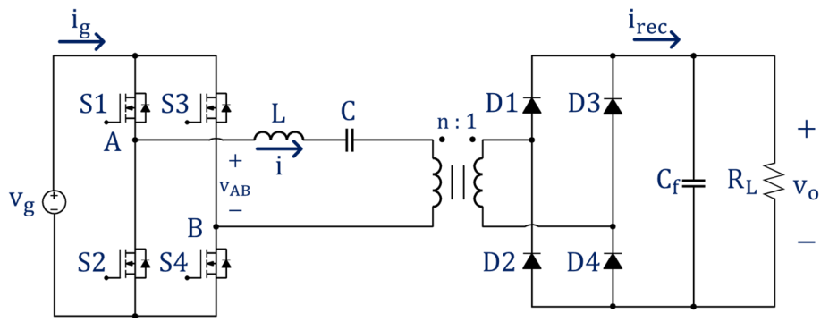
Figure 1 illustrates the equivalent circuit of a phase-shift full-bridge SRC. The input DC voltage v g is converted by the switching action of switches S 1 ~ S 4 into the AC inverter output voltage v A B , which is applied to the input of the resonant tank. The resonant tank consists of the resonant inductor L and resonant capacitor C and is connected to the primary side of a high-frequency isolation transformer with a turns ratio of n : 1 . The polarity of v A B determines the direction of the resonant-tank current i . This current is transferred to the secondary side of the transformer and, after full-wave rectification by D 1 ~ D 4 , appears as the rectified current i r e c . The rectified current i r e c charges and discharges the output filter capacitor C f , and delivers power to the load R L , while C f smooths the rectified waveform to produce the output DC voltage v o .
The extended describing function (EDF) is a modeling technique that approximates the waveforms of a nonlinear system by their fundamental components and analyzes the dynamic characteristics using slowly varying harmonic coefficients. This method is based on the fundamental approximation and harmonic balance theory. Among the small-signal models developed for accurate analysis of SRC dynamics, the EDF-based small-signal equivalent-circuit model proposed by Yang et al. [13] has been widely used. This model effectively captures the beat-frequency dynamics ω b e a t by retaining only the fundamental components of the resonant tank variables.
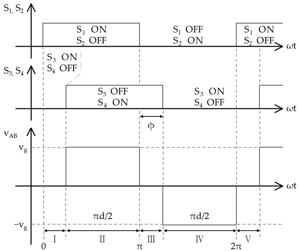
In previous studies, pulse frequency modulation (PFM) has mainly been used for output voltage regulation. In this approach, the inverter duty ratio d is fixed at unity, and the output voltage is controlled by adjusting the switching frequency ω s = 2 π f s [13,14]. In this case, the switching frequency must be varied according to the load condition or input voltage variation in order to maintain the nominal output voltage. Owing to this characteristic, a higher switching frequency may be required in a PFM SRC to regulate the output voltage under light load conditions, which can degrade the soft-switching performance and increase the switching loss. To overcome this limitation, this paper proposes the phase-shift scheme shown in Figure 2. In this scheme, the output is controlled by adjusting the effective duty ratio d, i.e., the phase shift, of the input-side bridge switches while maintaining the switching frequency near the resonant frequency ω o = 2 π f o .
Before deriving the small-signal model, the switching waveforms and each operating interval of the proposed phase-shift control scheme are briefly described with reference to Figure 2.
Figure 2 illustrates the switching waveforms of the full-bridge phase-shift control scheme. The waveforms can be divided into five operating intervals according to the switching operation. In the phase-shift control method, the output voltage is regulated by adjusting the phase-shift angle Φ between the two diagonal switch pairs while keeping the duty ratio of each switch constant.
Interval I corresponds to the state where switches S 1 and S 3 are ON and S 2 and S 4 are OFF. During this interval, the inverter output is short-circuited, and thus v A B becomes zero.
Interval II corresponds to the state where switches S 1 and S 4 are ON simultaneously, while S 2 and S 3 are OFF. During this interval, the inverter output voltage v A B becomes + v g .
In Interval III, S 2 and S 4 are turned ON simultaneously, whereas S 1 and S 3 are OFF. As in Interval I, the inverter output is short-circuited during this interval, and thus the inverter output voltage becomes zero.
In Interval IV, S 2 and S 3 are ON, whereas S 1 and S 4 are OFF. During this interval, the inverter output voltage v A B becomes v g .
Interval V repeats Interval I, and the previously described switching sequence repeats to generate an AC voltage. This AC voltage is the inverter output voltage and the input voltage applied to the resonant tank, i.e., v A B .
Based on the EDF-based approach introduced above, the phase-shift full-bridge SRC in Figure 1 is formulated in state-space form. As expressed in Equation (1), each variable is decomposed into its steady-state and perturbation components around the operating point. Here, i o represents the output-current perturbation treated as a disturbance input, and therefore its steady-state component is set to zero in Equation (1). The small-signal state equations in Equation (2) are then obtained by linearization under the small-signal assumption. The matrix terms in Equation (3), derived from the EDF-based formulation, are given in Equations (4)–(10).
v g = V g + v ^ g ,   d = D + d ^ ω s = Ω s + ω ^ s ,   i o = 0 + i ^ o
d x ^ d t = A x ^ + B u ^ y ^ = D x ^ + E u ^ x ^ = i ^ s   i ^ c   v ^ s   v ^ c   v ^ c f = v ^ o T u ^ = v ^ g   d ^   ω ^ s   i ^ o T y ^ = v ^ o   i ^ g T
A = R s / L Z s / L 1 / L 0 2 k s / L Z c / L R c / L 0 1 / L 2 k c / L 1 / C 0 0 G / C 0 0 1 / C G / C 0 0 k s / C f k c / C f 0 0 1 / R L C f B = k v / L k d / L B s / L 0 0 0 B c / L 0 0 0 E s / C 0 0 0 E c / C 0 0 0 0 1 / C f D = 0 0 0 0 1 I a 0 0 0 0 E = 0 0 0 0 0 I d 0 0
X e q = Ω s L 1 Ω s C ,   R e q = 8 n 2 π 2 R L
I a = 2 π s i n π D 2 ,   I d = I s c o s π D 2 k v = 4 π s i n π D 2 ,   k d = 2 V g c o s π D 2
I s = k v V g R e q X e q 2 + R e q 2 ,   I c = k v V g X e q X e q 2 + R e q 2 V s = k v V g Ω s C X e q X e q 2 + R e q 2 ,   V c = k v V g Ω s C R e q X e q 2 + R e q 2
k r s = k r c = R e q 2 X e q X e q 2 + R e q 2 ,   k s = 2 n π R e q X e q 2 + R e q 2 ,   k c = 2 n π X e q X e q 2 + R e q 2
R s = R e q X e q 2 X e q 2 + R e q 2 ,   R c = R e q R e q 2 X e q 2 + R e q 2
Z s = Ω s L k r s ,   Z c = Ω s L + k r c B s = L I c ,   B c = L I s E s = C V c ,   E c = C V s
G = Ω s C
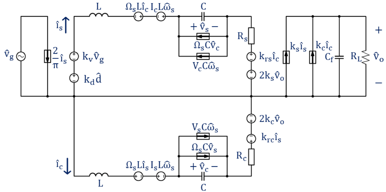
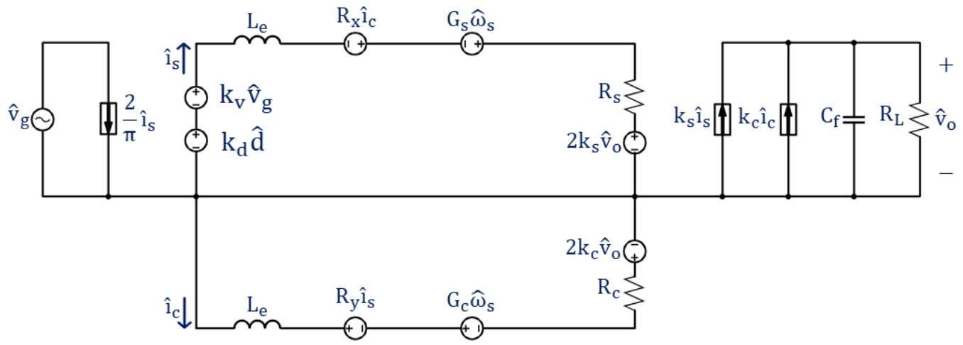
Figure 3 shows the fifth-order small-signal model derived using the EDF technique. This model is useful for state-space-based numerical analysis and simulation, but it becomes a structurally complex fifth-order system owing to the cross-coupling among the state variables. As a result, the transfer functions can only be obtained through numerical procedures, and analytical derivation is difficult.
Therefore, to enable more intuitive analysis and design while preserving the dominant resonant-tank dynamics, the fifth-order small-signal model is simplified to a third-order small-signal model. In particular, this order reduction exploits the property that the resonant capacitor can be interpreted as an equivalent inductor when the modulation frequency ω m is sufficiently lower than the switching frequency. In Section 3, the non-coupled equivalent circuit is then derived by eliminating the coupling terms among the state variables using the circuit equations and the superposition principle. This approach simplifies the derivation of the transfer functions, enables a small-signal model that can be expressed in analytical form, and allows the physical meaning of the circuit to be interpreted more intuitively.

2.2. Proposed Third-Order Equivalent Circuit

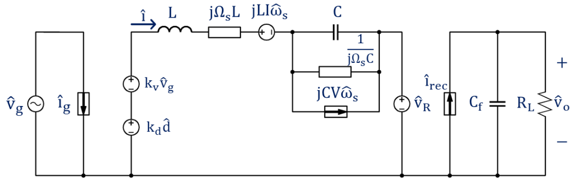
To derive the third-order small-signal model, the small-signal model in Figure 3 is reformulated as shown in Figure 4. Here, the impedances and dependent sources are represented in complex form, including the imaginary unit.
Although Figure 4 corresponds to a third-order model from the viewpoint of model order, its physical meaning is difficult to interpret intuitively because the impedances and dependent sources are expressed in complex form. Therefore, an additional transformation process is required to obtain a more intuitive equivalent circuit from which the transfer functions can be derived analytically.
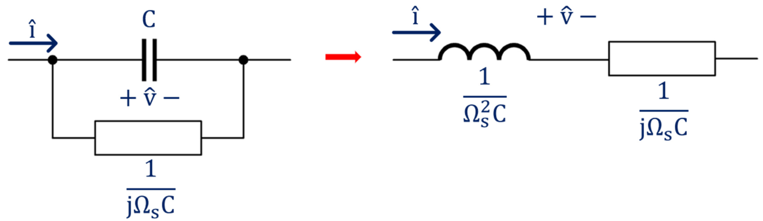
First, the capacitor branch and the constant term connected in parallel with it are transformed into an equivalent inductor and a series resistor. To do so, the dependent current source included in the capacitor branch must first be removed. When the switching frequency is kept constant, the perturbation in the switching frequency ω ^ s can be set to zero, so the dependent current source j C V ω ^ s can be removed. As a result, rearranging the voltage–current relation of the capacitor branch yields Equation (11).
By applying the condition in Equation (12), the term s 2 / Ω s 2 becomes sufficiently small to be neglected, and thus Equation (13) can be approximated in the form of Equation (13). Consequently, as illustrated in Figure 5, the capacitor can be interpreted as behaving like an inductor when Equation (12) is satisfied.
v ^ i ^ = 1 s C + j Ω s C = 1 j Ω s C s j Ω s + 1 = s j Ω s + 1 j Ω s C s j Ω s + 1 s j Ω s + 1 = s j Ω s + 1 j Ω s C 1 + s 2 Ω s 2
ω m Ω s ,   s Ω s 2 1
v ^ i ^ = 1 s C + j Ω s C s j Ω s + 1 j Ω s C = s Ω s 2 C + 1 j Ω s C
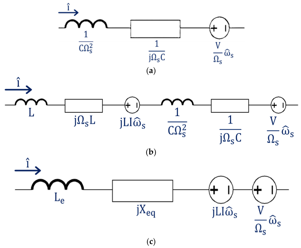
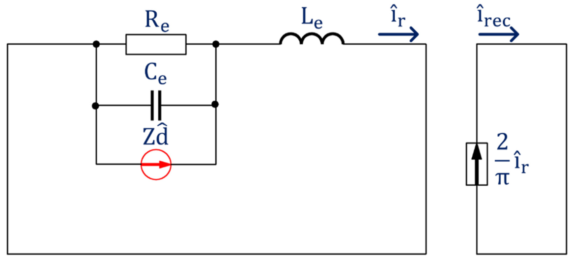
Next, the impedance and dependent current source connected in parallel with the capacitor can be interpreted as a Norton equivalent circuit. By applying Thevenin’s theorem, the capacitor branch can be transformed into an equivalent voltage source with a series impedance, as shown in Figure 6a. When this equivalent network is then combined with the remaining passive elements and dependent sources of the resonant tank, the circuit can be reduced to the minimum form shown in Figure 6c.
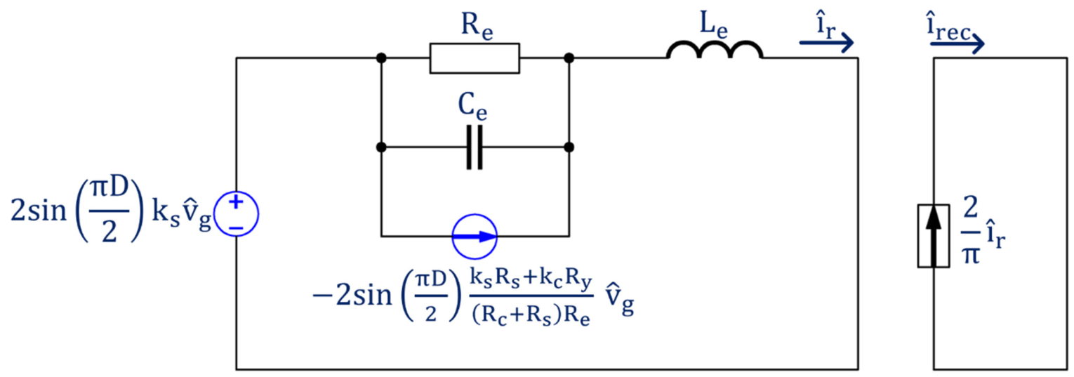
As a result, the fifth-order small-signal circuit model is reduced to the third-order small-signal equivalent-circuit model shown in Figure 7, and the parameters used for the equivalent-circuit simplification are defined in Equations (14)–(16).
Equations (14)–(16) define the parameters used in simplifying the equivalent circuit.
R x = X e q 3 X e q 2 + R e q 2 ,   R y = X e q X e q 2 + 2 R e q 2 X e q 2 + R e q 2
G s = B s + V s Ω s ,   G c = B c V c Ω s
L e = L + V s C Ω s 2 = L 1 + Ω o 2 Ω s 2 ,   C e = 1 L e Ω s Ω o 2 ,   R e = L e X e q Ω s Ω o R e q
Accordingly, as shown in Equation (17), the numerator and denominator of the fifth-order transfer function G 5 t h can be decomposed into third-order polynomials and neglected terms, denoted by N and D , introduced during the approximation process. To evaluate the accuracy and validity range of the third-order transfer function G 3 r d , the ratio between the fifth-order and third-order transfer functions F s is defined as in Equation (18).
G 3 r d = N 3 r d D 3 r d ,   G 5 t h = N 5 t h D 5 t h = N 3 r d + Δ N D 3 r d + Δ D
F s = G 5 t h ( s ) G 3 r d ( s ) = N 5 t h D 3 r d D 5 t h N 3 r d = ( N 3 r d + Δ N ) D 3 r d ( D 3 r d + Δ D ) N 3 r d = 1 + Δ N N 3 r d 1 + Δ D D 3 r d
The model in Figure 7, derived through the above simplification process, is a linearized small-signal model intended for the analysis of small perturbations around the steady-state operating point. The validity range of the proposed third-order small-signal model is evaluated through the ratio between the fifth-order and third-order transfer functions defined in Equation (18). In the low-frequency region, the approximation condition in Equation (12) is well satisfied, and therefore, the proposed model agrees well with the fifth-order model. In contrast, as the frequency approaches the switching frequency, the condition in Equation (12) is no longer well satisfied, and the mismatch may increase. Therefore, the proposed model is suitable for controller design and low-frequency dynamic analysis, but it has limitations in high-frequency dynamic analysis and direct analysis of transient behavior. The validity of the third-order small-signal model was verified through the transfer function ratio defined in Equation (18) and frequency-response comparisons, and the results are presented in Section 4.

3. Non-Coupled Equivalent Circuit

Proposed Non-Coupled Equivalent Circuit

Although the third-order small-signal equivalent model is simpler than the fifth-order model, it still contains coupling terms among the state variables, and therefore, the desired transfer functions are difficult to derive directly.
To derive the non-coupled equivalent circuit, KVL and KCL are first applied to the coupled third-order model in Figure 7 to formulate the relationship between the sine and cosine components of the resonant-tank current. The perturbation paths are then separated using Thevenin’s theorem and the superposition principle, yielding the non-coupled third-order circuit. The coupling term appearing in the sine path is defined in Equation (19), and the related variables are defined in Equation (20).
Based on the resulting non-coupled circuit, each transfer function is derived by retaining only the perturbation source of interest while setting the remaining perturbations to zero. In this way, the effects of the input voltage, duty ratio, and output voltage perturbations can be analyzed independently through the corresponding transfer paths.
R x i ^ c = i ^ s R e 1 C e 1 ,   i ^ c = R y s L e + R c i ^ s
The parameter expressions for the equivalent impedances of the non-coupled circuit in Equations (20) and (21) show that the proposed formulation can reproduce the beat-frequency dynamics.
R e 1 = R x R y R c ,   C e 1 = L e R x R y
R e = R e 1 + R s 1 + R e 1 C e 1 R s / L e = R x R y + R x R c R s + R c ,   C e = C e 1 R e 1 R e 1 + R s = L e R x R y + R s R c
ω b e a t = Ω s Ω o
In addition, as the switching frequency approaches the resonant frequency, the beat-frequency double pole in the phase-shift non-coupled circuit splits, so the overall circuit can be effectively interpreted as exhibiting second-order behavior.
The rectifier output current i ^ r e c is used as the reference variable to formulate the non-coupled circuit. By choosing it as the reference variable, the effects of the input voltage v ^ g , output voltage v ^ o , and duty d ^ perturbations on the rectifier output current through the resonant tank can be organized independently. Therefore, for each case, each transfer function G v g s , G v d s , G v o s can be derived by retaining only the perturbation of interest and setting all other perturbations to zero, and the results are summarized in Equation (23).
i ^ r e c ( s ) = G v g s v ^ g s + G v d s d ^ s + G v o ( s ) v ^ o ( s )
In addition, the analytical derivation procedure for obtaining the transfer functions corresponding to each perturbation from the third-order equivalent small-signal model is briefly presented in Equations (24)–(30), thereby summarizing the overall procedure for obtaining the non-coupled equivalent circuit.
G v g s in Equation (24) represents the effect of the input voltage perturbation on the output current. That is, it is the transfer function from the DC input voltage perturbation to the rectifier output current perturbation, and it quantifies how the input voltage variation is reflected in the output current through the resonant tank and the rectifier. Equation (25) briefly represents the derivation process of the corresponding equivalent circuit, from which the equivalent circuit in Figure 8 is obtained.
G v g ( s ) = i ^ r e c ( s ) v ^ g ( s ) v ^ o = 0 , d ^ = 0
s L e + R s i ^ s R x i ^ c = 4 π sin π D 2 v ^ g s L e + R c i ^ c + R y i ^ s = 0 i ^ s = 4 π sin π D 2 s L e + R c v ^ g s L e + R s s L e + R c + R x R y , i ^ c = 4 π s i n π D 2 R y v ^ g s L e + R s s L e + R c + R x R y i ^ r e c ( s ) v ^ g ( s ) = 4 π X e q 2 + R e q 2 s i n π D 2 R e q s L e + R e q + X e q 2 s L e s L e + R e q + X e q 2
G v d s in Equation (26) represents the effect of the duty ratio (phase-shift) perturbation on the output current. That is, it is the transfer function from the control perturbation to the rectifier output current perturbation, and it quantifies how the change in the control variable modifies the fundamental component of the bridge output voltage and consequently changes the current delivered to the output through the resonant tank.
G v d ( s ) = i ^ r e c ( s ) d ^ ( s ) v ^ g = 0 , v ^ o = 0
In the case of a PFM SRC, the corresponding control-to-current transfer path is generally expressed as a transfer function with the switching frequency perturbation as the input [14]. Both the PFM SRC and the phase-shift SRC describe the control effect on the output current delivered through the resonant tank, but the dominant control path depends on the modulation scheme.
In PFM control, the frequency variation directly changes the tank impedance, and thus the frequency path becomes the dominant control path. By contrast, in phase-shift control, the duty ratio variation changes the effective driving voltage component applied to the tank, and therefore the duty path becomes the dominant control path.
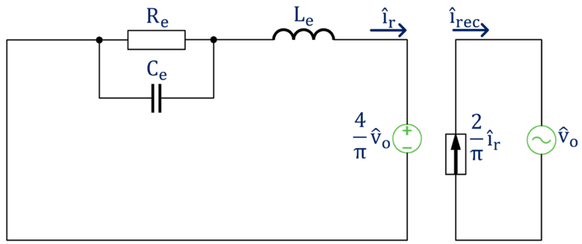
Equation (28) defines the gain used to represent the effect of the duty ratio (phase-shift) perturbation in the form of a dependent current source in the non-coupled equivalent circuit. This term acts as an equivalent current source and is ultimately used to derive the Control (Duty)-to-Output transfer function. Therefore, by following the circuit derivation process briefly expressed in Equation (27), the circuit shown in Figure 9 can be obtained.
s L e + R s i ^ s R x i ^ c = 2 V g cos π D 2 d ^ s L e + R c i ^ c + R y i ^ s = 0 i ^ s = 2 V g c o s π D 2 d ( s L e + R c ) s L e + R s s L e + R c + R x R y , i ^ c = 2 V g R y c o s π D 2 d ^ s L e + R s i ^ r e c ( s ) d ^ ( s ) = 2 X e q 2 + R e q 2 V g c o s π D 2 R e q s L e + R e q + X e q 2 s L e s L e + R e q + X e q 2
Z = π V g c o s π D 2 k s s L e + R c k c R y X e q 2
G v o s in Equation (29) represents the effect of the output voltage perturbation on the output current. When the output voltage changes because of a load variation, the resulting perturbation shifts the operating point of the resonant tank and the rectifier, and this transfer function represents the corresponding rectifier output current response. Accordingly, the corresponding circuit can be constructed as shown in Figure 10.
G v o ( s ) = i ^ r e c ( s ) v ^ o ( s ) v ^ g = 0 , d ^ = 0
s L e + R s i ^ s R x i ^ c + 2 k s v ^ o = 0 s L e + R c i ^ c + R y i ^ s + 2 k c v ^ o = 0 i ^ s = 2 k s s L e + R c 2 k c R x s L e + R s s L e + R c + R x R y v ^ o , i ^ c = 2 k s R y 2 k c ( s L e + R s ) s L e + R s s L e + R c + R x R y v ^ o i ^ r e c ( s ) v ^ o ( s ) = 4 π s L e + R e q s L e s L e + R e q + X e q 2
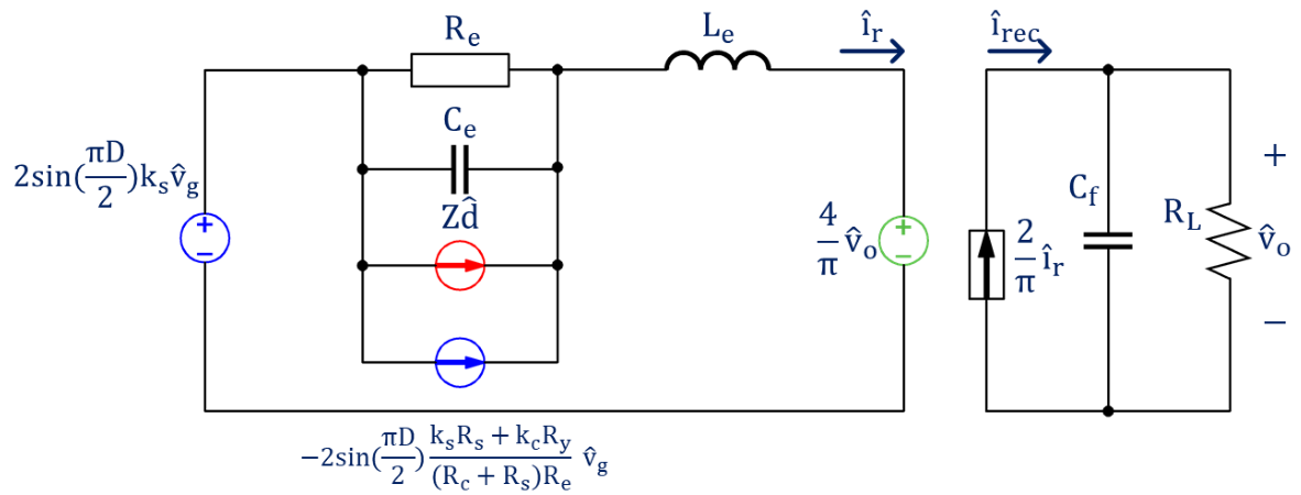
Finally, by combining the equivalent circuits in Figure 8, Figure 9 and Figure 10 using the superposition principle, the final non-coupled equivalent circuit in Figure 11 can be derived. The resulting circuit enables the transfer paths associated with the input, output, and duty perturbations to be analyzed independently. Since this derivation is based on a linearized small-signal model, the proposed circuit is suitable for controller design, low-frequency dynamic analysis, and the analysis of small perturbations near the operating point. However, it has limitations in high-frequency dynamic analysis and in the direct prediction of large-signal conditions and transient states.
Based on Figure 11, the transfer functions can be derived analytically, unlike in the conventional fifth-order small-signal model, and the explicit expressions for the Control (Duty)-to-Output transfer function v ^ o s / d ^ s , Line-to-Output transfer function v ^ o s / v ^ g s , output impedance Z o s , and input impedance Z i n s are presented in Equations (31)–(34).
v ^ o ( s ) v ^ g ( s ) d ^ = 0 = 4 π sin π D 2 [ k s s L e + R c k c R y ] R L 1 + s C f R L s L e s L e + R e q + X e q 2 + 2 [ k s k c R y + k c 2 s L e + R c + k s 2 ( s L e + R c ) ] R L
v ^ o ( s ) d ^ ( s ) v ^ g = 0 = 2 V g cos π D 2 [ k s s L e + R c k c R y ] R L 1 + s C f R L s L e s L e + R e q + X e q 2 + 2 [ k s k c R y + k c 2 s L e + R c + k s 2 ( s L e + R c ) ] R L
Z o s = R L ( s 2 L e 2 + s L e R e q + X e q 2 ) s 2 L e 2 + s L e R e q + X e q 2 1 + s C f R L + R e q ( s L e + R e q )
Z i n s = π 2 8 s i n 2 π D 2 ( s 2 L e 2 + s L e R e q + X e q 2 ) 1 + s C f R L + R e q ( s L e + R e q ) s 2 L e C f R L + s L e + s C f R L R e q 3 R e q 2 + X e q 2 + R e q

4. Simulation and Experimental Results

4.1. Simulation

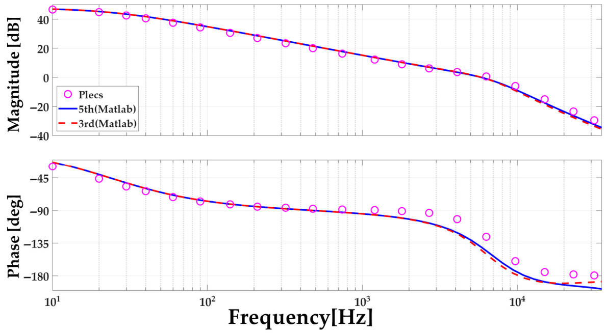
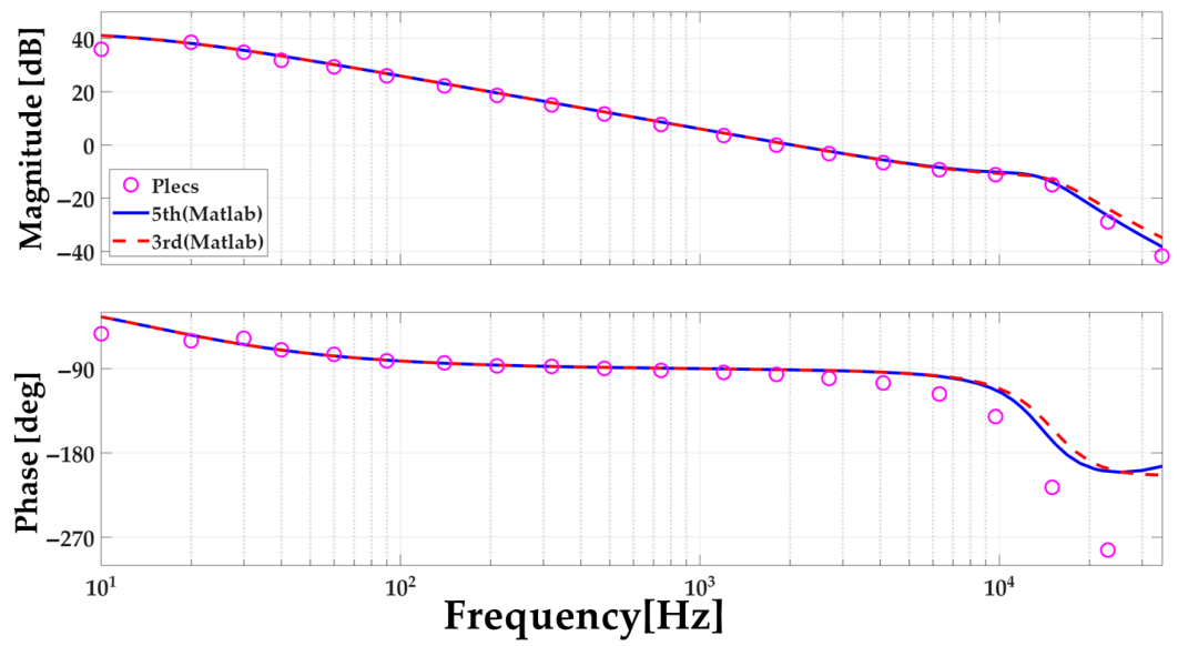
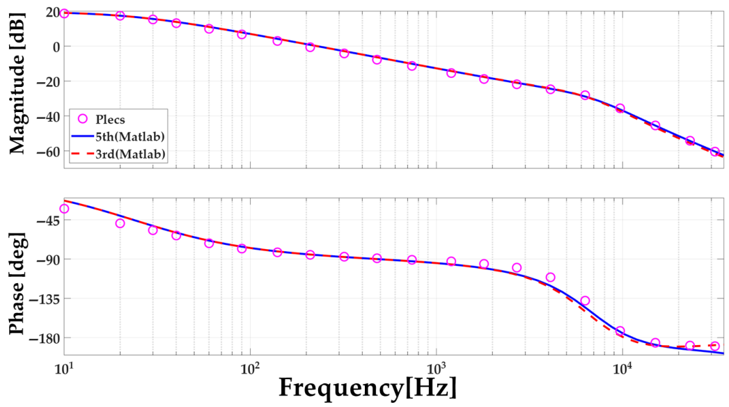
The derived third-order non-coupled equivalent-circuit model was analyzed to obtain the corresponding transfer functions in explicit analytical form. To verify the validity of the proposed model, the equations of the fifth-order small-signal model, i.e., Equations (2) and (3), were first implemented in MATLAB (R2025b), and their low-frequency small-signal frequency responses were compared with those of the proposed third-order equivalent-circuit model. In addition, a circuit-based PLECS (4.7.5) model was used as a reference model, and the low-frequency small-signal frequency responses of the fifth-order and third-order small-signal models obtained in MATLAB were compared. Furthermore, the validity range of the proposed third-order non-coupled equivalent-circuit model was evaluated using the ratio between the fifth-order and third-order transfer functions defined in Equation (18). To verify the validity of the proposed equivalent-circuit model under different operating conditions, the normalized switching frequency F s n f s / f o was set to F s n = 0.9 f s = 62.82 kHz and F s n = 1.2 f s = 83.76 kHz. The parameters used in the simulation are listed in Table 1.
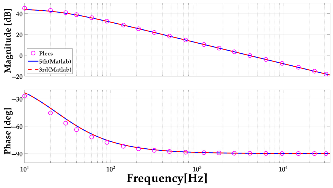
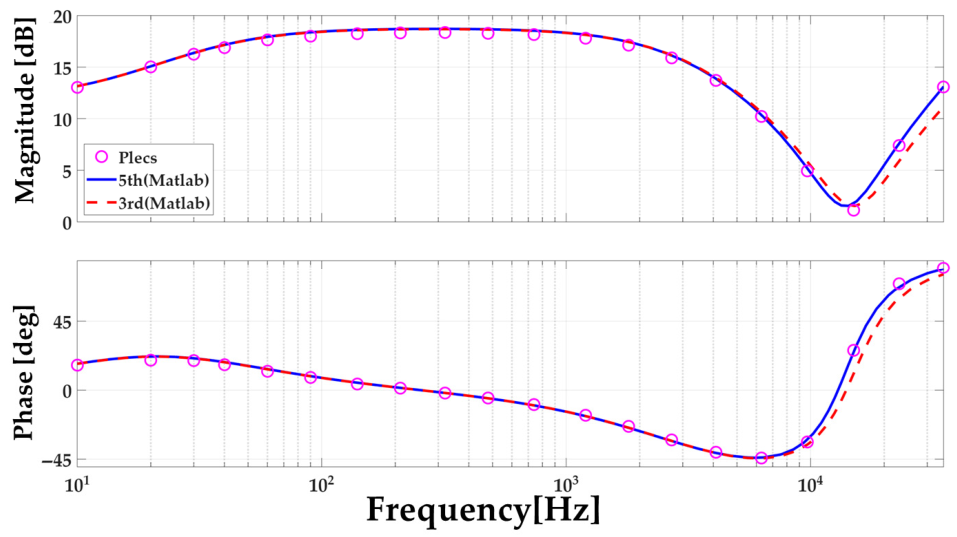
Figure 12 and Figure 13 compare the Control (Duty)-to-Output transfer functions obtained from the proposed third-order model and the fifth-order model with the PLECS results. The operating points were set to F s n = 0.9 ,   D = 0.358 ,   R L = 400   Ω and F s n = 1.2 ,   D = 0.544 ,   R L = 400   Ω , respectively. It can be seen that the three results show very good overall agreement.
Figure 14 and Figure 15 show the Line-to-Output transfer functions, which were evaluated at the same operating points as the Control (Duty)-to-Output transfer functions. In this case as well, the three results agree well with one another.
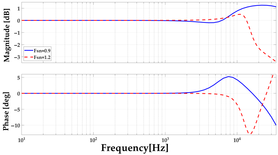
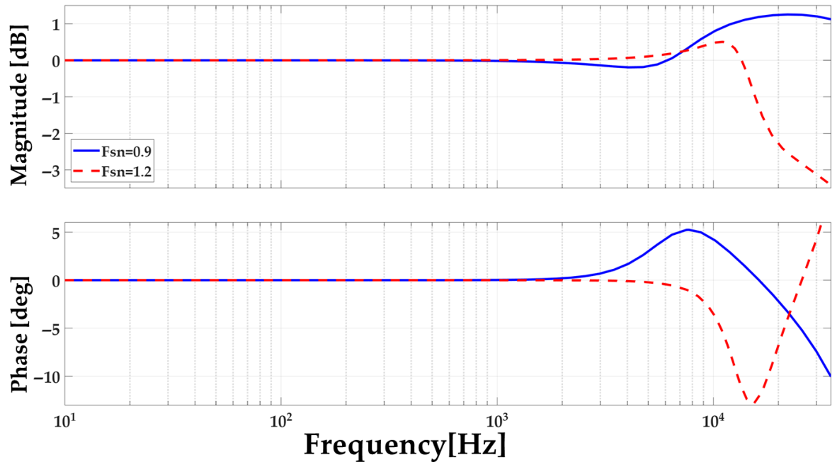
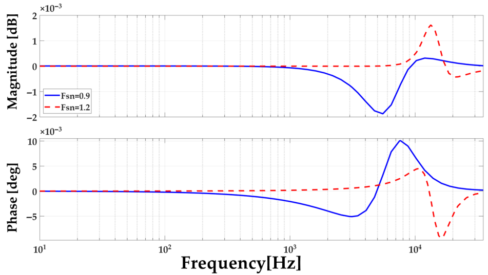
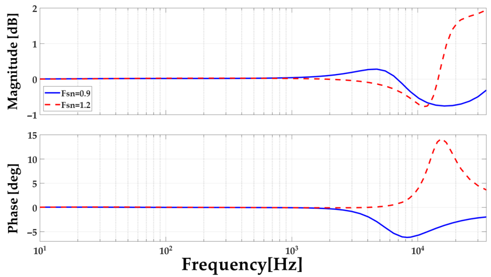
Figure 16 and Figure 17 show the comparison results of the Line-to-Output and Control (Duty)-to-Output transfer functions of the fifth-order and third-order models using the ratio defined in Equation (18). The reason why the two figures exhibit similar trends is that, except for the gain coefficients, the numerator and denominator polynomials of the two transfer functions are identical. In the low-frequency region, the effects of the higher-order terms omitted in the approximation process are sufficiently small, yielding F s = 1 , i.e., F ( s ) d B 0 dB. So, the ratio between the two models is close to unity. In contrast, as the frequency approaches the switching frequency, the approximation condition in Equation (12) is no longer satisfied, and the relative influence of the omitted terms in Equation (15) increases, leading to a mismatch between the two models.
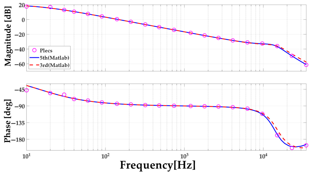
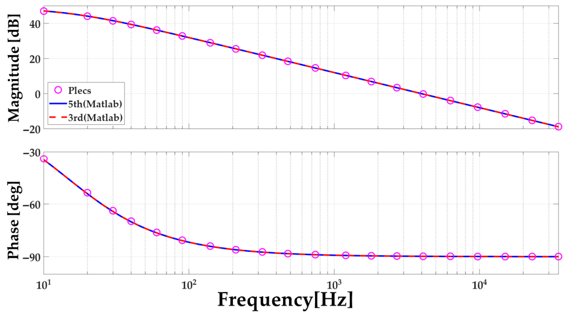
Figure 18 and Figure 19 show the output impedance responses, while Figure 20 and Figure 21 show the input impedance responses.
Figure 22 and Figure 23 show the transfer function ratios between the fifth-order and third-order models for the output and input impedances. As in Figure 16 and Figure 17, the ratio between the two models is close to unity in the low-frequency region, yielding F s = 1 , i.e., F ( s ) d B 0 dB. But the mismatch between the two models gradually becomes more pronounced as the frequency approaches the switching frequency.
In the simulation results, the conventional fifth-order model agrees very well with the PLECS results, confirming the validity of the formulation of the higher-order model. In addition, the proposed third-order model agrees well with the fifth-order model within its validity range, thereby confirming the accuracy and validity of the proposed model.

4.2. Experimental Results

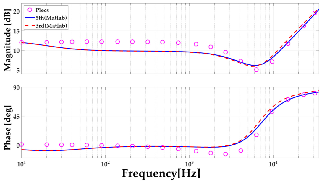
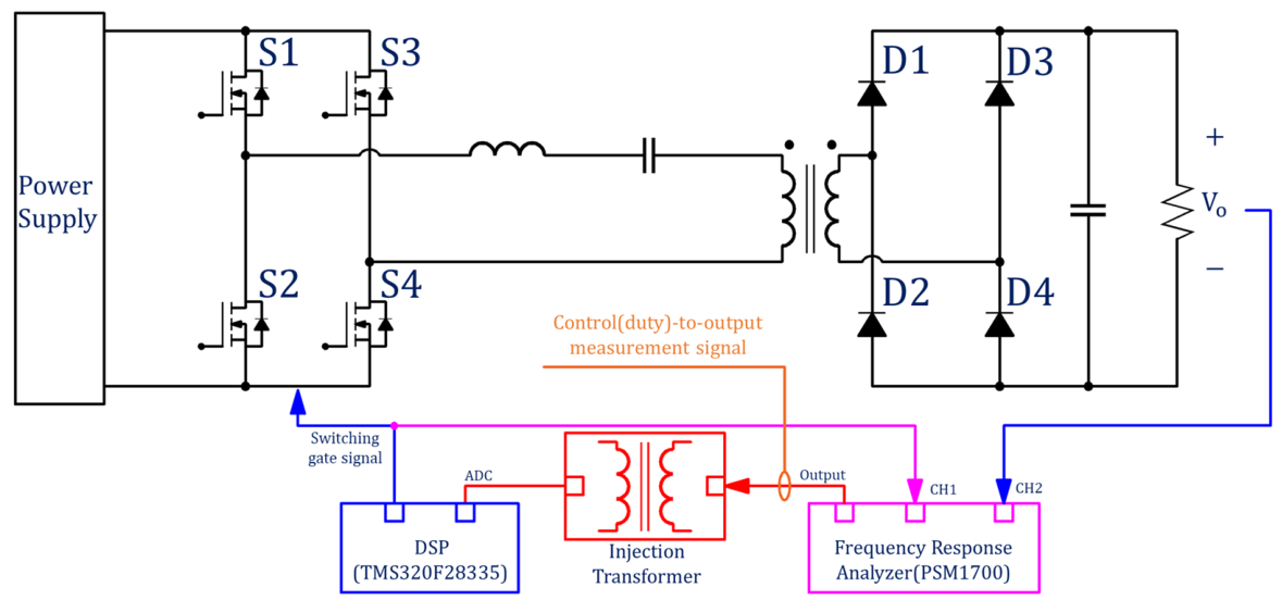
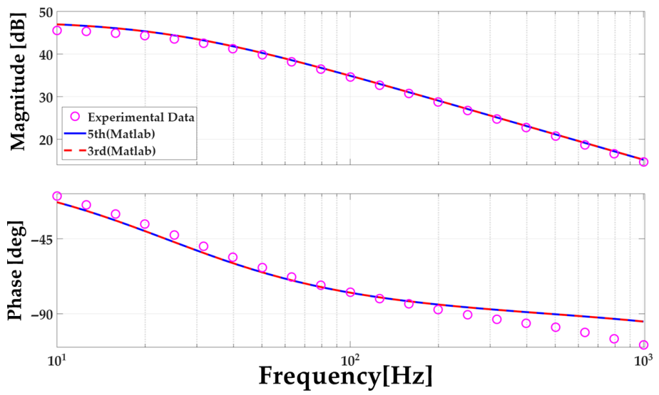
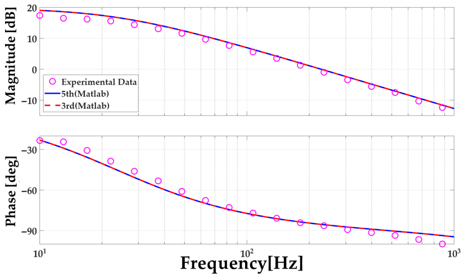
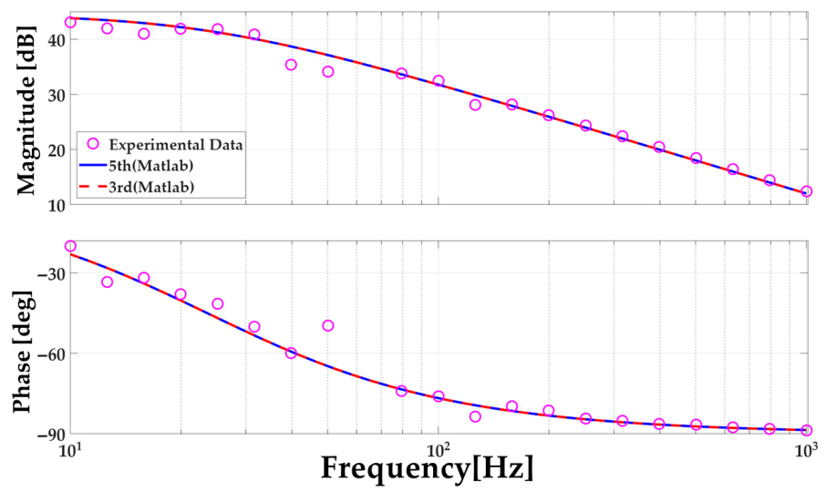
To experimentally verify the low-frequency small-signal frequency-response characteristics predicted by the proposed model, the transfer function responses obtained from the simulations were compared with the experimental measurements. The SRC was implemented using the parameters listed in Table 1. The gate signals were generated using DSP control board based on the TMS320F28335 DSP (Texas Instruments, Dallas, TX, USA), and the power stage was built using GS66508T GaN transistors (Infineon Technologies, Neubiberg, Germany, 650 V, 30 A). The rectifier was implemented using MURS160-13-F diodes (Diodes Incorporated, Plano, TX, USA, 600 V, 1 A). The resonant inductor was fabricated by winding five turns on a powder magnetic core (ChangSung, Incheon, Republic of Korea), and film capacitors were used for both the resonant capacitor and the output capacitor. The frequency responses were measured using a PSM1700 Frequency Response Analyzer (Newtons4th Ltd., Leicester, UK). Figure 24 shows the hardware configuration of the PSM1700 Frequency Response Analyzer used to measure the Control (Duty)-to-Output transfer function. The excitation output of the analyzer is fed into the ADC of the DSP board, and the DSP superimposes it on the reference duty command to generate the transistor gate signals. To compensate for the phase delay, the gate signal was measured on CH1, and the output voltage was sensed through the analyzer and measured on CH2. The transfer function measurements were performed at the operating point with a normalized switching frequency of 1. The Line-to-Output transfer function and output impedance were also measured at the same operating point. In the model, parasitic and loss elements such as the output capacitance of the GS66508T GaN transistor R D S , the winding resistances of the inductor and transformer, and the capacitor loss factors were neglected. Figure 25, Figure 26 and Figure 27 show the comparison results. Although mismatches appear in some frequency regions, the overall trends of the gain and phase responses agree well. These differences are attributed to the neglected loss elements and the difference in operating point between simulation and experiment, and they become relatively more noticeable in the higher-frequency region. Nevertheless, the proposed small-signal model remains valid for low-frequency dynamic analysis and controller design.
Figure 25, Figure 26 and Figure 27 show the comparison results. Although mismatches appear in some frequency regions, the overall trends of the gain and phase responses of each transfer function agree with one another.

5. Conclusions

Various small-signal models, including EDF-based small-signal equivalent-circuit models, have been proposed for resonant converters. However, in most conventional small-signal models, the transfer functions can only be obtained through complex numerical procedures, which limits intuitive physical interpretation of the circuit. To overcome this limitation, this paper proposes a simplified non-coupled third-order small-signal equivalent-circuit model for the phase-shift SRC based on the conventional EDF-based fifth-order model. The proposed model exploits the property that the resonant capacitor can be interpreted as an equivalent inductor when the modulation frequency is sufficiently lower than the switching frequency and applies the superposition principle to eliminate the coupling terms among the state variables. As a result, the circuit structure is significantly simplified, enabling analytical derivation of the key transfer functions without relying on conventional numerical procedures and allowing more intuitive physical interpretation of the circuit. The present derivation method is conceptually extendable to similar resonant topologies; however, because the circuit structure and the coupling relationships among the state variables depend on the target converter, the model equations must be reformulated and the order-reduction procedure must be newly carried out for each topology.
In addition, the validity range of the proposed model was evaluated through the ratios of the key transfer functions between the conventional fifth-order model and the proposed third-order model, and the causes of the mismatches observed in the high-frequency region were also analyzed. In the low-frequency region, the assumption that the switching frequency is sufficiently higher than the modulation frequency is well satisfied, so the influence of the higher-order terms omitted in the approximation process is very small, and the mismatch between the fifth-order model and the proposed model is negligible. However, as the frequency approaches the switching frequency, this approximation condition is no longer satisfied, and the influence of the omitted terms increases, thereby increasing the mismatch between the fifth-order model and the proposed model. Therefore, the proposed model is useful for controller design and low-frequency dynamic analysis, but it has limitations in the direct analysis of large-signal conditions and transient states. Finally, the accuracy and validity of the proposed model were verified through comparisons of the low-frequency small-signal frequency responses obtained from MATLAB, PLECS, and experimental measurements.

Author Contributions

Conceptualization, Y.-J.C.; methodology, Y.-J.C.; software, Y.-J.C.; validation, Y.-J.C.; Formal analysis, Y.-J.C.; investigation, Y.-J.C. and K.-J.L.; Resources, K.-J.L.; writing—original draft preparation, Y.-J.C. and N.-Y.K.; writing—review and editing, Y.-J.C. and K.-J.L.; Visualization, Y.-J.C. and N.-Y.K.; Supervision, K.-J.L.; Project administration, K.-J.L. All authors have read and agreed to the published version of the manuscript.

Funding

This work was supported by the Korea Institute of Energy Technology Evaluation and Planning (KETEP) grant funded by the Ministry of Trade, Industry and Energy (MOTIE) (RS-2024- 00394769). This work was supported by the Human Resources Development of the Korea Institute of Energy Technology Evaluation and Planning (KETEP) grant funded by the Korean government. (No. 20224000000070).

Data Availability Statement

The original contributions presented in this study are included in the article. Further inquiries can be directed to the corresponding author.

Conflicts of Interest

The authors declare no conflict of interest.

References

  1. Shen, Y.; Zhao, W.; Chen, Z.; Cai, C. Full-Bridge LLC Resonant Converter with Series-Parallel Connected Transformers for Electric Vehicle On-Board Charger. IEEE Access 2018, 6, 13490–13500. [Google Scholar] [CrossRef]
  2. Ryu, S.-H.; Kim, D.-H.; Kim, M.-J.; Kim, J.-S.; Lee, B.-K. Adjustable Frequency–Duty-Cycle Hybrid Control Strategy for Full-Bridge Series Resonant Converters in Electric Vehicle Chargers. IEEE Trans. Ind. Electron. 2014, 61, 5354–5362. [Google Scholar]
  3. Kwon, Y.D.; Freijedo, F.D.; Wijekoon, T.; Liserre, M. Series Resonant Converter-Based Full-Bridge DC–DC Partial Power Converter for Solar PV. IEEE J. Emerg. Sel. Top. Power Electron. 2024, 2, 1719–1729. [Google Scholar] [CrossRef]
  4. Zhao, B.; Yu, Q.; Sun, W. Extended-Phase-Shift Control of Isolated Bidirectional DC–DC Converter for Power Distribution in Microgrid. IEEE Trans. Power Electron. 2012, 27, 4667–4680. [Google Scholar] [CrossRef]
  5. Costa, L.F.; Buticchi, G.; Liserre, M. A Family of Series-Resonant DC–DC Converter with Fault-Tolerance Capability. IEEE Trans. Ind. Appl. 2018, 54, 335–344. [Google Scholar] [CrossRef]
  6. Steigerwald, R.L. A comparison of half-bridge resonant converter topologies. IEEE Trans. Power Electron. 1988, 3, 174–182. [Google Scholar] [CrossRef]
  7. Park, G.-M.; Lee, K.-J. Small-Signal Modeling of Asymmetric PWM Control Based Series Resonant Converter. Electronics 2025, 14, 3394. [Google Scholar] [CrossRef]
  8. Liu, B.; Tang, Y.; Ge, L.; Niu, J. Feedforward Compensation for Phase-Shifted Full-Bridge DC–DC Converter Under Peak Current Mode Control. IEEE Trans. Power Electron. 2024, 39, 6840–6851. [Google Scholar] [CrossRef]
  9. Safaee, A.; Karimi-Ghartemani, M.; Jain, P.K.; Bakhshai, A. Time-Domain Analysis of a Phase-Shift-Modulated Series Resonant Converter with an Adaptive Passive Auxiliary Circuit. IEEE Trans. Power Electron. 2016, 31, 7714–7734. [Google Scholar] [CrossRef]
  10. Sanders, S.R.; Noworolski, J.M.; Liu, X.Z.; Verghese, G.C. Generalized averaging method for power conversion circuits. IEEE Trans. Power Electron. 1991, 6, 251–259. [Google Scholar] [CrossRef]
  11. Vorperian, V. Approximate small-signal analysis of the series and the parallel resonant converters. IEEE Trans. Power Electron. 1989, 4, 15–24. [Google Scholar] [CrossRef]
  12. Yue, X.; Wang, X.; Blaabjerg, F. Review of Small-Signal Modeling Methods Including Frequency-Coupling Dynamics of Power Converters. IEEE Trans. Power Electron. 2019, 34, 3313–3328. [Google Scholar] [CrossRef]
  13. Yang, E.X.; Lee, F.C.; Jovanovic, M.M. Small-signal modeling of series and parallel resonant converters. In Proceedings of the APEC ’92 Seventh Annual Applied Power Electronics Conference and Exposition, Boston, MA, USA, 23–27 February 1992; pp. 785–792. [Google Scholar]
  14. Tian, S.; Lee, F.C.; Li, Q. A Simplified Equivalent Circuit Model of Series Resonant Converter. IEEE Trans. Power Electron. 2016, 31, 3922–3931. [Google Scholar] [CrossRef]
  15. Tian, S.; Lee, F.C.; Li, Q. Equivalent Circuit Modeling of LLC Resonant Converter. IEEE Trans. Power Electron. 2020, 35, 8833–8845. [Google Scholar] [CrossRef]
  16. Chang, C.-H.; Chang, E.-C.; Cheng, C.-A.; Cheng, H.-L.; Lin, S.-C. Small Signal Modeling of LLC Resonant Converters Based on Extended Describing Function. In Proceedings of the 2012 International Symposium on Computer, Consumer and Control, Taichung, Taiwan, 4–6 June 2012; IEEE: Piscataway, NJ, USA, 2012. [Google Scholar]
  17. Chang, C.-H.; Cheng, C.-A.; Cheng, H.-L. Modeling and Design of the LLC Resonant Converter Used as a Solar-Array Simulator. IEEE J. Emerg. Sel. Top. Power Electron. 2014, 2, 833–841. [Google Scholar] [CrossRef]
  18. Maheshwari, A.; Karakaya, F.; Banerjee, A.; Donnal, J.S. Control Architecture for LLC Resonant Converters with High Input Disturbance Rejection Capability Using Output Diode Current. IEEE Trans. Power Electron. 2025, 40, 652–664. [Google Scholar] [CrossRef]
  19. Nakagaki, A.; Hiraki, E.; Umetani, K.; Masataka, I.; Yoshimura, Y. Actual Circuit Verification of LC Series Resonant Converter with Power Factor Control for Effective Power in Load regulation. In Proceedings of the IECON 2024—50th Annual Conference of the IEEE Industrial Electronics Society; IEEE: New York, NY, USA, 2024; pp. 1–7. [Google Scholar]
  20. Singh, P.; Chaudhary, K. Multiport Bidirectional Converter with Resonant and PWM Modes for Drives Applications. In Proceedings of the 2024 IEEE International Conference on Intelligent Systems, Smart and Green Technologies (ICISSGT); IEEE: New York, NY, USA, 2024; pp. 1–6. [Google Scholar]
  21. Ai, Y.; Liu, J.; Chen, S.; Pei, C. A Small-Signal Modeling Method for LLC Resonant Converter Based on Time-Domain Correction. IEEE Trans. Power Electron. 2024, 39, 10792–10806. [Google Scholar] [CrossRef]
Figure 1. Equivalent circuit of full-bridge SRC.
Electronics 15 01491 g001
Figure 2. v A B waveform of phase-shift modulation.
Electronics 15 01491 g002
Figure 3. Small-signal model of 5th-order SRC.
Electronics 15 01491 g003
Figure 4. Small-signal model of 5th-order SRC in complex form.
Electronics 15 01491 g004
Figure 5. Equivalent conversion of resonant tank under ω m Ω s .
Electronics 15 01491 g005
Figure 6. Simplified equivalent circuit of resonant tank: (a) resonant capacitor branch transformed using Thevenin’s theorem. (b) circuit obtained from (a). (c) Combining the inductance and complex impedances.
Electronics 15 01491 g006
Figure 7. Simplified equivalent small-signal model of 3rd-order SRC.
Electronics 15 01491 g007
Figure 8. Non-coupled equivalent circuit for G v g .
Electronics 15 01491 g008
Figure 9. Non-coupled equivalent circuit for G v d .
Electronics 15 01491 g009
Figure 10. Non-coupled equivalent circuit for G v o .
Electronics 15 01491 g010
Figure 11. Final non-coupled equivalent circuit of SRC.
Electronics 15 01491 g011
Figure 12. Control (Duty)-to-Output transfer function F s n = 0.9 ,   D = 0.358 ,   R L = 400   Ω .
Electronics 15 01491 g012
Figure 13. Control (Duty)-to-Output transfer function F s n = 1.2 ,   D = 0.544 ,   R L = 400   Ω .
Electronics 15 01491 g013
Figure 14. Line-to-Output transfer function F s n = 0.9 ,   D = 0.358 ,   R L = 400   Ω .
Electronics 15 01491 g014
Figure 15. Line-to-Output transfer function F s n = 1.2 ,   D = 0.544 ,   R L = 400   Ω .
Electronics 15 01491 g015
Figure 16. Ratio of the 5th-order and 3rd-order transfer function F s = G v d 5 ( s ) / G v d 3 ( s ) .
Electronics 15 01491 g016
Figure 17. Ratio of the 5th-order and 3rd-order transfer function F s = G v g 5 ( s ) / G v g 3 ( s ) .
Electronics 15 01491 g017
Figure 18. Output impedance F s n = 0.9 ,   D = 0.358 ,   R L = 400   Ω .
Electronics 15 01491 g018
Figure 19. Output impedance F s n = 1.2 ,   D = 0.544 ,   R L = 400   Ω .
Electronics 15 01491 g019
Figure 20. Input impedance F s n = 0.9 ,   D = 0.358 ,   R L = 400   Ω .
Electronics 15 01491 g020
Figure 21. Input impedance F s n = 1.2 ,   D = 0.544 ,   R L = 400   Ω .
Electronics 15 01491 g021
Figure 22. Ratio of the 5th-order and 3rd-order transfer function F s = Z o 5 ( s ) / Z o 3 ( s ) .
Electronics 15 01491 g022
Figure 23. Ratio of the 5th-order and 3rd-order transfer function F s = Z i 5 ( s ) / Z i 3 ( s ) .
Electronics 15 01491 g023
Figure 24. Experimental hardware configuration for measuring Control (Duty)-to-Output response.
Electronics 15 01491 g024
Figure 25. Experimental verification of Control (Duty)-to-Output transfer function F s n = 0.9 ,   D = 0.358 ,   R L = 400   Ω .
Electronics 15 01491 g025
Figure 26. Experimental verification of Line-to-Output transfer function F s n = 0.9 ,   D = 0.358 ,   R L = 400   Ω .
Electronics 15 01491 g026
Figure 27. Experimental verification of output impedance F s n = 0.9 ,   D = 0.358 ,   R L = 400   Ω .
Electronics 15 01491 g027
Table 1. System parameters.
V g 10 VL5.2 μH
C f 40 μFC1 μF
n1/24 f o 69.8 kHz
Disclaimer/Publisher’s Note: The statements, opinions and data contained in all publications are solely those of the individual author(s) and contributor(s) and not of MDPI and/or the editor(s). MDPI and/or the editor(s) disclaim responsibility for any injury to people or property resulting from any ideas, methods, instructions or products referred to in the content.