1. Introduction
The modular multilevel converter (MMC) [
1] topology has been used for years in high-voltage transmission line conversion [
2] and has already been introduced as suitable for use in high-voltage pulsed applications [
3]. This topology exhibits superior performance in generating high-voltage pulses and provides a potential alternative to conventional topologies employed in applications such as pulsed power plasma generators. The Dense Plasma Focus device at the Institute of Plasma Physics and Lasers (IPPL) of the University Research and Innovation Center of the Hellenic Mediterranean University served as the test case in our previous work [
3,
4]. Despite the superior performance demonstrated there, the initial design presents a notable limitation: it does not fully exploit the inherent modularity [
5] of the MMC topology. This design bypasses one of the primary advantages of MMC, namely its ability to distribute voltage stress across multiple, cascaded submodules. In this first implementation, both the power supply and the driving transformers of the IGBTs (insulated gate bipolar transistors) must withstand the full output pulse voltage. Although the MMC topology [
6] is already widely used in electrical power conversion handling voltages of several hundred kV [
7], modularity in modules driving and parameter sensing is typically lacking in these applications [
8]. In most cases optical fibers are used to overcome such issues [
9].
This work demonstrates that the MMC topology can be effectively employed to realize a full modular configuration using a serially propagated triggering scheme for pulsed-power applications. Furthermore, it establishes the basis for an MMC-based trigger generator approach that may represent an alternative to the solid-state linear transformer driver (SSLTD) technology [
10] currently used in certain high-voltage, high-current pulsed generator systems. When applied to such systems, the proposed approach may offer significant advantages, including simpler construction, improved scalability, and the elimination of specialized ferromagnetic materials.
In this paper, a novel MMC-based trigger generator is presented, featuring full modularity and expandability, while requiring insulation rated only for a single module voltage [
11]. Owing to its scalability, the proposed design can be adapted to generate high-voltage pulses of practically any amplitude, as well as to operate at high repetition rates. To evaluate the performance of the proposed design, a new trigger generator was developed for use with the IPPL’s Z-Pinch machine [
12]. The generator, composed of five submodules utilizing IGBTs and foil capacitors, replaces an obsolete thyratron-based trigger unit. Each submodule handles 3 kV, resulting in a high-voltage output pulse with a peak amplitude of approximately 15 kV.
To highlight the advantages of this approach in spark-gap trigger generators employing forward converters, it can be compared with other semiconductor-based trigger generators reported in the literature. When transformers with high step-up ratios are used, the associated parasitic inductance typically increases, which adversely affects the slope of the output pulse. For example, J. Wang [
13] uses a step-up ratio of 1:150 to achieve a 45 kV pulse peak, while C. S. Reddy [
14] uses a step-up ratio of 1:40 to reach 15 kV. In this work, the trigger generator was developed to operate with a transformer having a step-up ratio of only 1:5, already installed into the Marx Bank, to achieve the 75 kV required for spark-gap breakdown. In [
13], the resulting output pulse rise time is in the microsecond range, which increases the jitter of spark-gap breakdown, especially considering that the breakdown voltage may vary with pressure or temperature conditions. Furthermore, a slower voltage rise increases the energy stored in the transformer core, degrades primary–secondary coupling due to a higher core magnetic field, and increases insulation stress because of the longer exposure to high voltage. Consequently, high step-up ratios often lead to more complex transformer designs. The proposed trigger generator achieves a significantly faster voltage rise, thereby mitigating these limitations and improving spark-gap triggering performance.
2. Design Considerations
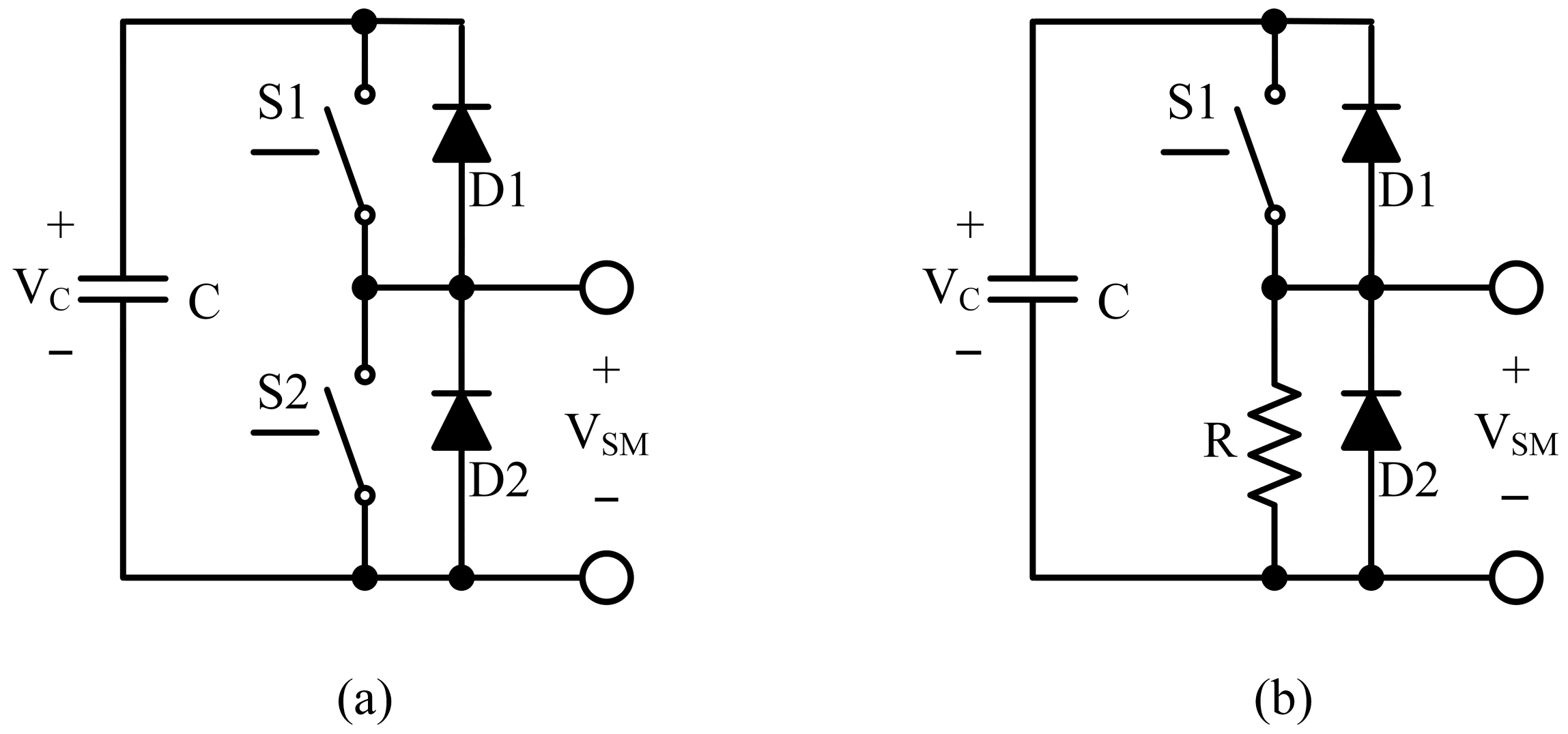
For the MMC to achieve full modularity and expandability in high-voltage pulsed applications, it is essential to enable inter-module exchange of input signal and power supply. In single-pulse or low-repetition-rate applications, the capacitor charging voltage can be exchanged between submodules. However, for high-repetition-rate applications, it is preferable for each submodule to generate its own capacitor charging voltage using its internal power supply. The most common submodule configuration for single-polarity applications is shown in
Figure 1a. It uses a totem-pole pair of switches (Half-Bridge Sub-module, HB-SM) to set its output either to 0 V or to the capacitor charging voltage (V
C). In pulsed power applications where the return current is negligible and the turn-off time is not critical, the modified submodule shown in
Figure 1b can be employed. This design eliminates the requirement for dead time during switching, reduces the number of switching components, and simplifies the overall control [
15]. If higher repetition rates are required, the Half-Bridge Submodule can be used.
A convenient and effective method for distributing the input signal to the submodules is through the use of optical fibers. They provide excellent electrical isolation, negligible input-output capacitance, and sufficiently fast signal transfer [
16]. Optical emitters can be connected in parallel, enabling control of all the submodules with the input signal simultaneously at maximum speed. However, this approach is not employed here due to its limitation in achieving full modularity, as the addition of each submodule would require modifications on the input side for the fiber connection. Moreover, independent driving through parallel optical fibers could also influence the shape of the output high-voltage pulse.
In this work, each submodule features an optocoupler that isolates the input signal, while the optocoupler’s output forwards the signal to the next submodule. Although this communication scheme introduces a propagation delay, all the submodules can be synchronized to switch simultaneously by employing programmable delay units. A specific delay is assigned to each submodule according to its position in the chain, ensuring that simultaneous switching occurs once the input signal reaches the final submodule.
Power transfer between submodules is achieved using transformers. The amount of power transferred by each transformer varies depending on the submodule’s position within the chain. For a given power level, the mass of a transformer decreases as its operating frequency increases. Therefore, by employing high-frequency power transfer, the transformer size can be significantly reduced. This approach also eliminates the need to decrease transformer mass as power requirements decrease, allowing all transformers to be of the same size, regardless of the power they transfer.
The capacitor charging voltage of each submodule is generated independently from its own power supply [
17]. This approach enables fast capacitor charging and supports high repetition rates. For single-shot operation or low repetition rates, all the capacitors can instead be charged from a common converter [
18]. Typically, when the capacitor charging voltage is sufficiently high, the forward voltage drop (conduction voltage) across any number of diodes can be considered negligible. As a result, a high-voltage diode can effectively transfer the capacitor charging voltage between submodules [
15].
3. Experimental Setup
To experimentally evaluate the performance of the proposed design, a high-voltage pulse generator unit was developed. The Z-Pinch machine at IPPL [
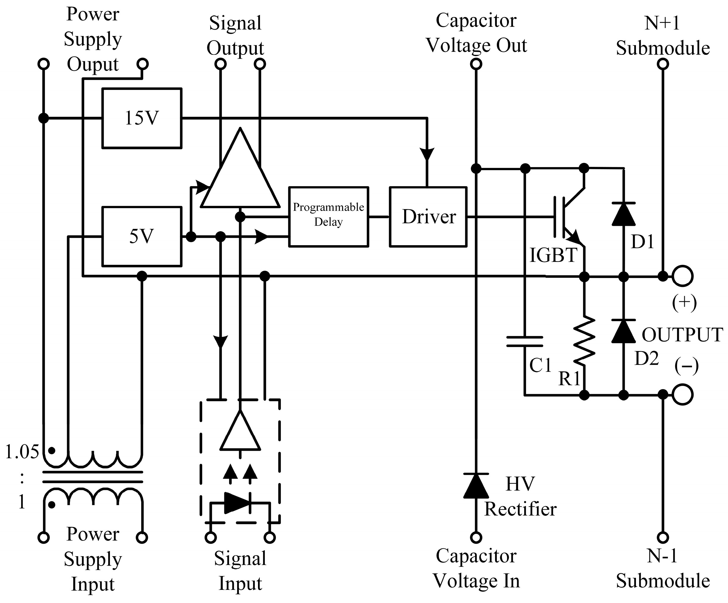
12] is normally triggered by a generator that produces 15 kV pulses using a thyratron electronic tube and a custom-built oil capacitor designed for high-voltage pulse applications. The Z-Pinch triggering process operates in a single-shot mode. To replace the existing trigger generator, the proposed submodule block diagram is presented in
Figure 2.
A 66 kHz pulse with convenient amplitude is applied to the “Power Supply Input” of each submodule. A 1:1.05 ratio transformer is used to propagate this pulse to the next submodule and compensate for the voltage drop. DC voltages of 5 V and 15 V are produced within each submodule to supply the digital circuit and the IGBT drive circuit, respectively. The “Signal Input” of each submodule is a 200 ns pulse, which is propagated through optocouplers to the next submodule. A Programmable Delay unit compensates for the propagation delay between each unit and drives the IGBT drive circuit. The capacitor voltage is propagated and shared through a High-Voltage (HV) Rectifier Diode between the submodules.
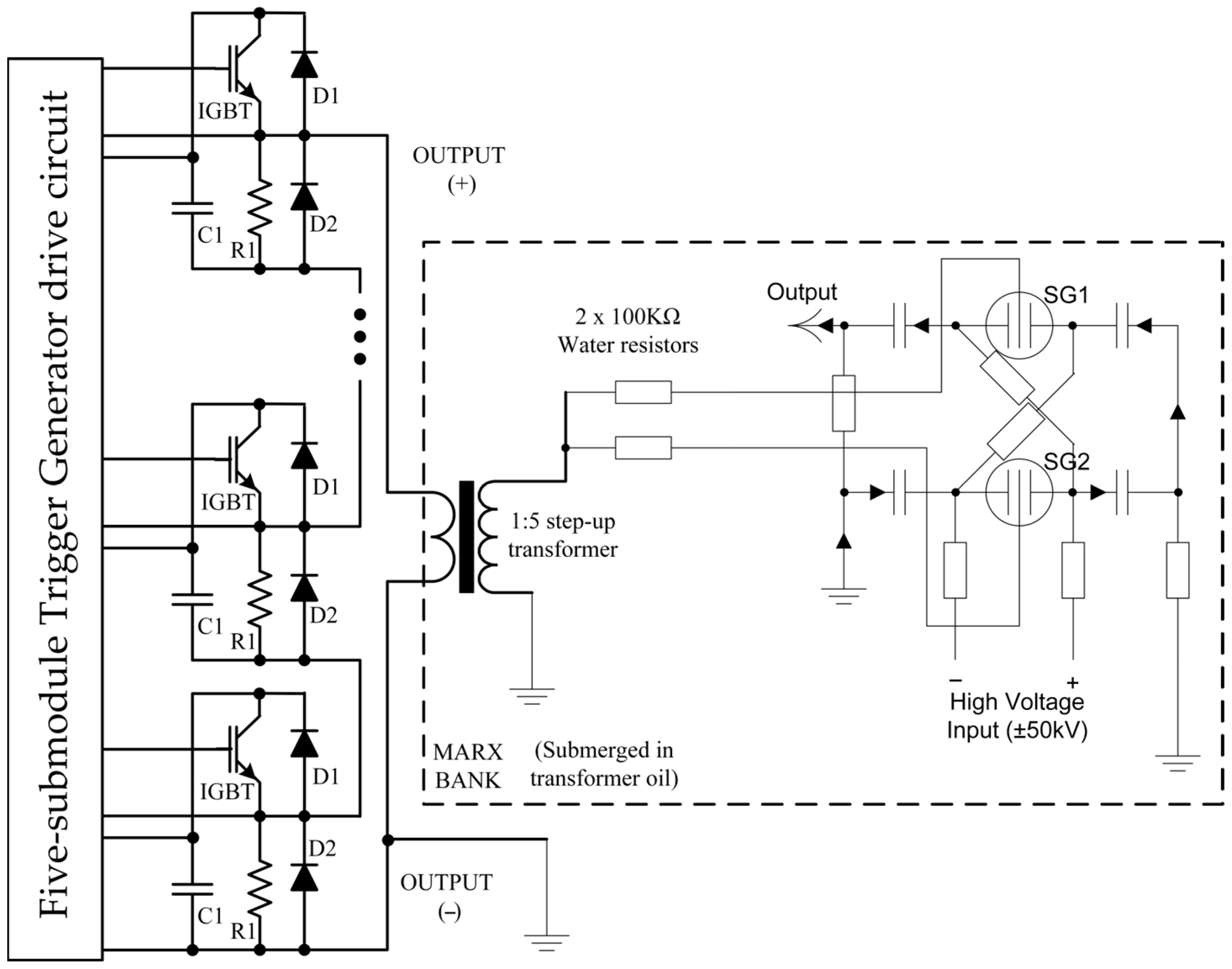
Within the submodules, diodes D1 and D2 are implemented using two 5VUZ52 low-voltage diodes connected in series. The load of the trigger unit cannot be assumed to be purely ohmic or inductive. A transmission line (50 Ω coaxial cable) connects the trigger unit to the Marx Bank, which also incorporates a transformer with a step-up ratio of 1:5 to increase the voltage to 75 kV for spark-gap breakdown. After the end of the trigger pulse and the breakdown of the spark gaps, a high current is induced at the output of the trigger unit due to the high voltage present on the spark-gap trigger electrode in the Marx Bank. This current is typically characterized by significant ringing. The placement of diodes D1 and D2 at the output stage is intended to protect the IGBTs from these effects. D1 operates as a freewheeling diode, providing a controlled path for reverse or transient currents and limiting overvoltage stress across the switches. D2 assists in managing current flow during post-pulse ringing events.
For the HV Rectifier, an HV5 diode is employed. The submodules’ capacitors (C1) consist of two WIMA FKP1 47 nF, 6 kV polypropylene film capacitors connected in parallel. The HV Rectifiers of all the submodules form a series-connected diode string with the corresponding submodule capacitor (C1) connected to each node. Since the charging voltage is significantly higher than the cumulative forward voltage drop of the five series-connected diodes, this drop can be considered negligible. Resistor R1 ensures that each submodule output remains at 0 V under open-circuit conditions and also provides the necessary current path to charge the capacitor (C1) of the subsequent submodule (N + 1) in the cascade.
For signal isolation, the high-speed digital optocoupler TLP2366 was used. The TLP2366 optocoupler features an input LED on-state current threshold of typically 0.9 mA, while for high-speed operation, a quiescent current of 0.35 mA was adjusted to flow through the LED in its off state.
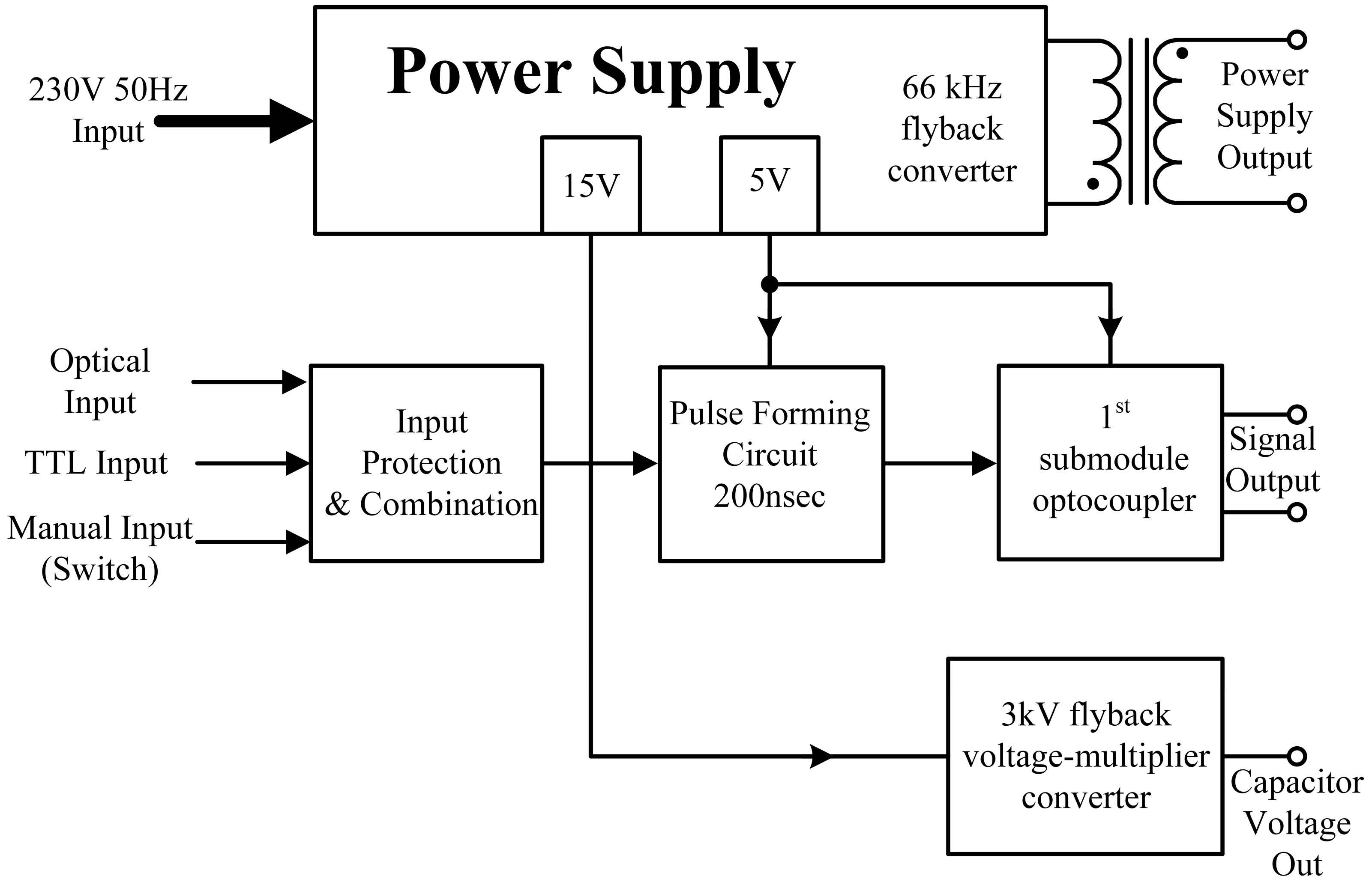
A Main Module was designed to manage the trigger generator’s input signals and provide the required control and supply voltage signals for the submodules. This module also generates the Submodules’ Capacitor Voltage. During the unit development, the IXYS IXG65I3300KN IGBTs were selected as the switching units for the submodules, as they were readily available and offered an excellent performance-to-cost ratio. These IGBTs are highlighted in “IXYS POWER Semiconductors Highlights” as a fast solution, and their performance has been verified in the laboratory. Although primarily designed for electronic ignition systems in vehicles, where turn-off is more critical, they also exhibit strong turn-on performance, making them suitable for this application. In the present system, the rise time of the generated pulse and any delays introduced by the trigger generator are not critical. The Z-Pinch machine at IPPL [
12] is synchronized using a signal from the Pulse Forming Line (PFL), specifically after the spark gaps, and therefore, the trigger generator does not affect the overall system timing. The Main Module design features a TTL input, an optical input, and a manual trigger switch. The input signal is processed by a pulse-forming circuit and then is transferred to the submodules with a pulse width of approximately 200 nanoseconds. The Main Module incorporates a flyback converter to generate the necessary low voltages for its operation and to power the submodules. Additionally, it includes a dedicated flyback voltage multiplier converter [
19] that produces the 3 kV Capacitor Voltage required for charging the submodules’ capacitors. The block diagram of the Main Module is shown in
Figure 3.
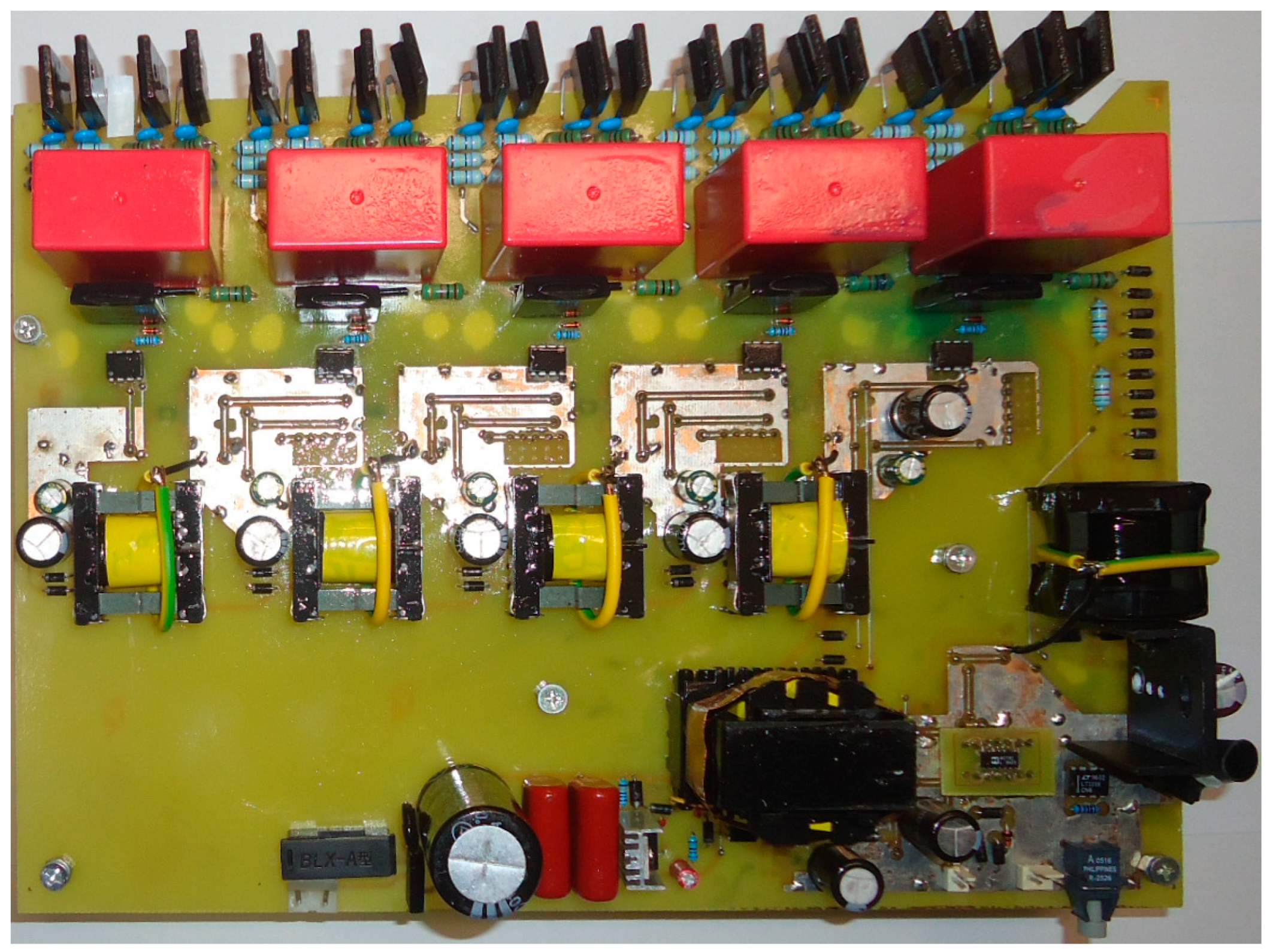
Through a series of circuit simplifications and design compromises, the authors successfully integrated the entire trigger generator circuit onto an A4-sized printed circuit board (PCB). A top-down view of the experimental prototype PCB is shown in
Figure 4. It should be noted that not all the components are visible in this view, as the additional five capacitors and several surface-mounted components are located on the bottom side of the board.
Electronic design follows well-established circuit design principles; therefore, detailed parameter derivation is beyond the scope of this work. To facilitate understanding of the implementation, the main components used in the prototype, along with a brief description of their respective functions, are summarized in
Table 1.
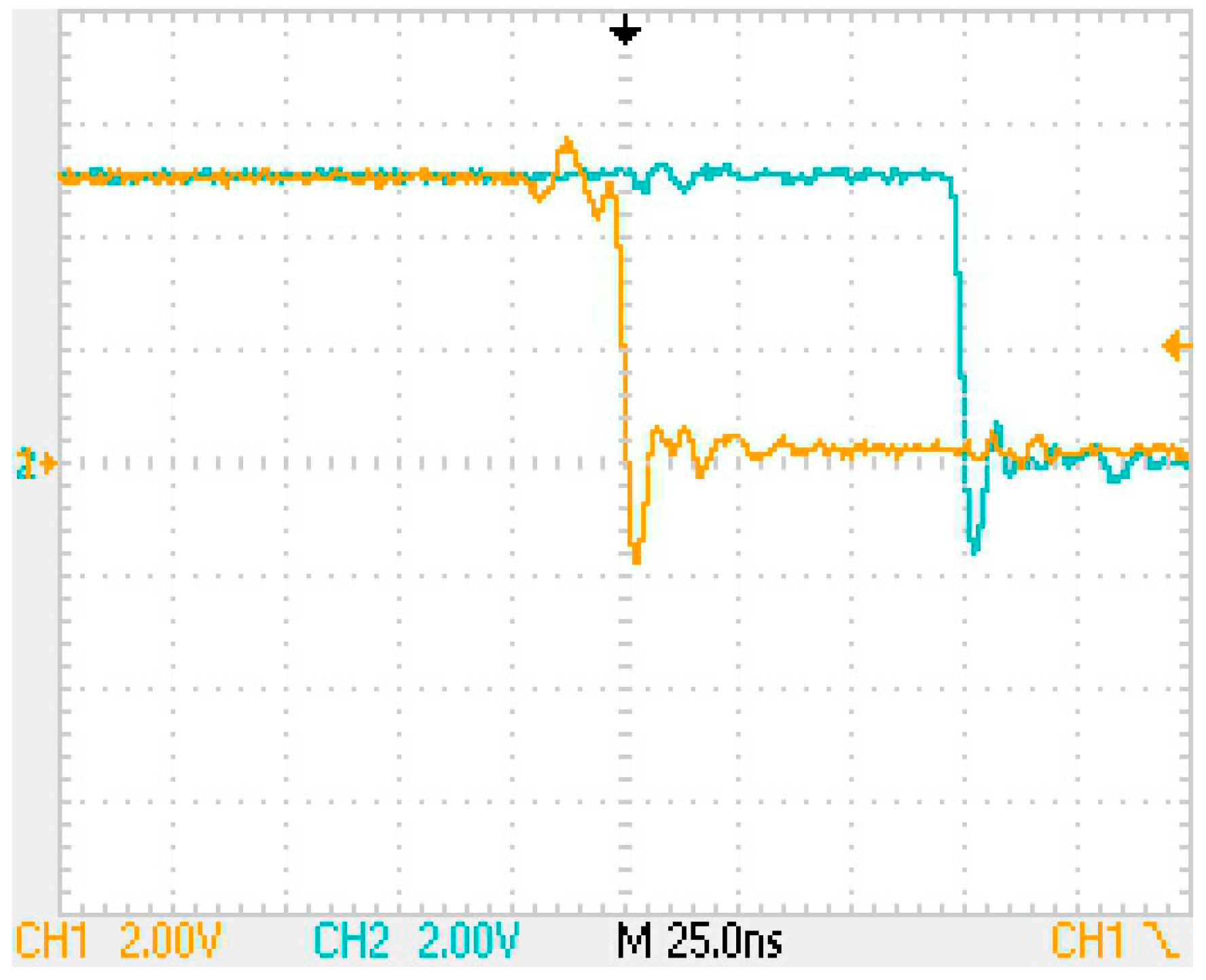
This configuration resulted in a total propagation delay of approximately 75 nanoseconds, measured from the Signal Output of the Main Module to the optocoupler output of the final (fifth) submodule, as illustrated in
Figure 5. Significantly, this total propagation delay is comparable to the rise time of a single IGBT. Consequently, the programmable delay line ICs (DS1023-50) were omitted from the final trigger generator implementation, simplifying the design without compromising performance.
The prototype is designed to replace the thyratron-based trigger unit of the Z-pinch machine at IPPL [
12].
Figure 6 shows the overall circuit system configuration of the trigger generator connected to the spark gaps of the Marx Bank. The Marx Bank of the Z-Pinch machine incorporates a critical 1:5 step-up transformer located inside the oil-filled enclosure, and its removal was not considered. This component increases the 15 kV input pulse to 75 kV, which effectively triggers the spark gaps. It is constructed using two EPCOS U 93 Transformer Ferrite Cores and features 10 turns in its primary winding. The transformer primary winding serves as the load of the trigger generator until spark-gap breakdown occurs.
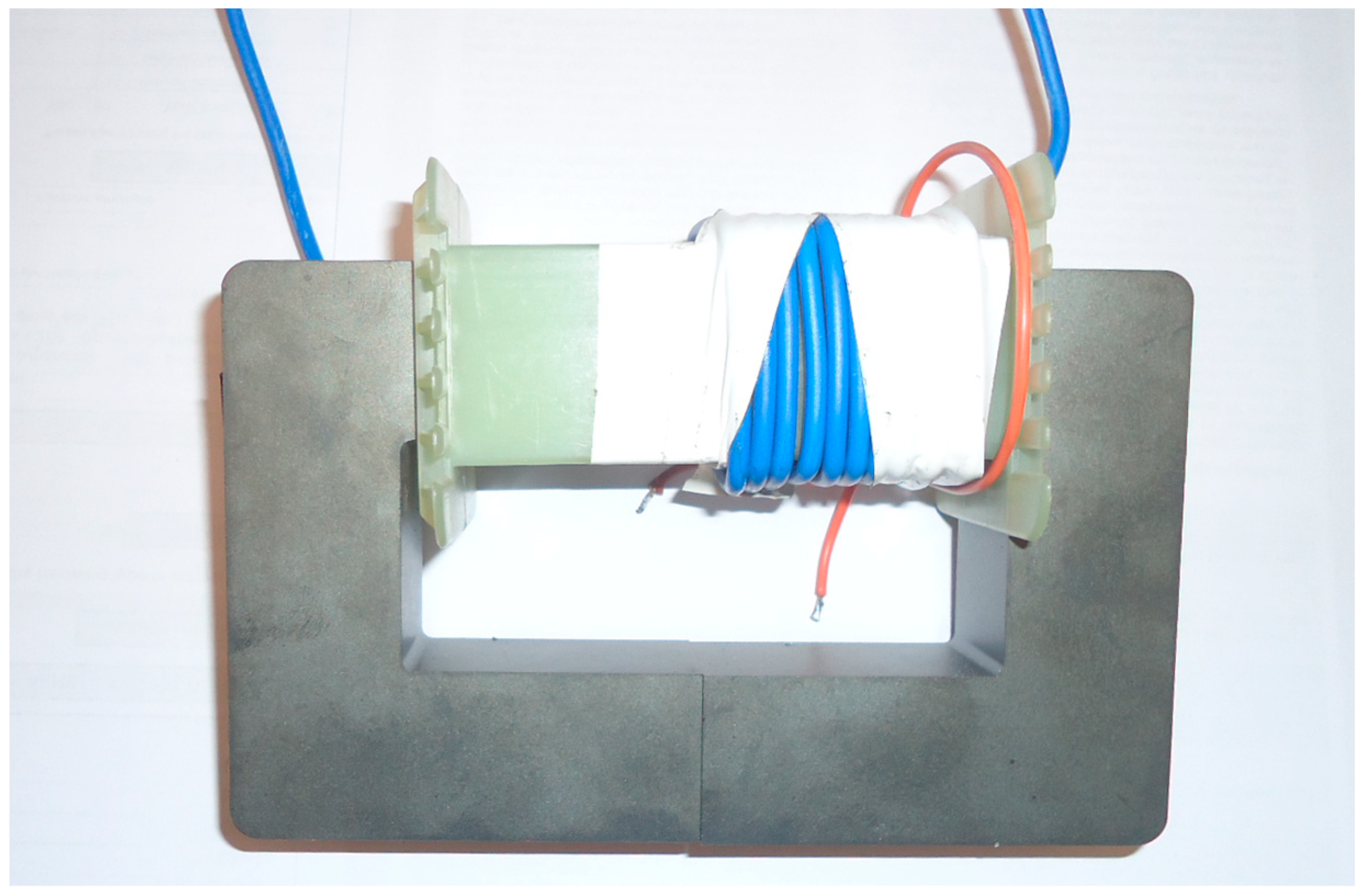
For development and testing purposes, the same primary winding was also constructed to be used as a load on the laboratory bench, as illustrated in
Figure 7. A key design consideration for the proposed trigger generator is the relatively slower switching speed of IGBTs compared to thyratrons. To mitigate the potential decrease in output pulse voltage due to the partial capacitor discharge during the IGBT’s rise time, the proposed trigger generator employs a higher total capacitance.
4. Results and Discussion
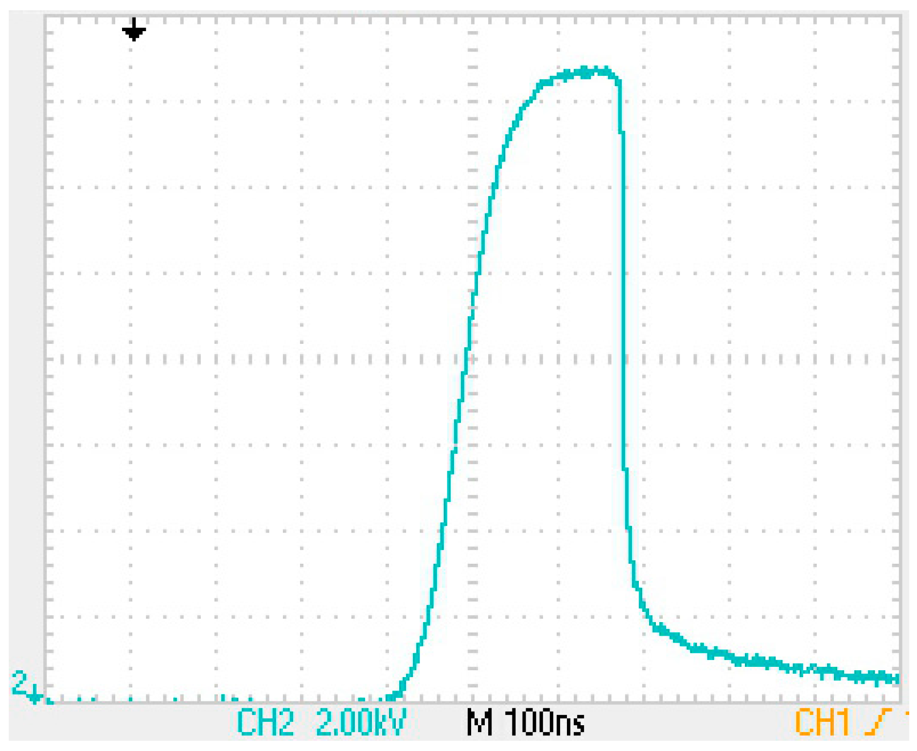
The trigger pulse generator was initially tested using a 10-turn coil wound on an EPCOS U93 transformer ferrite as the load in order to verify its proper operation. This preliminary measurement confirmed that the trigger generator produced the expected high-voltage pulse. To record the high-voltage output pulse, a single-turn secondary winding was added to the ferrite core, forming a 10:1 measurement transformer. A 100:1 oscilloscope probe (HAMEG HZ53) was then used, resulting in an overall signal attenuation of 1000:1. The signals were recorded using a Tektronix TDS2024B digital oscilloscope.
Figure 8 illustrates the input trigger point (black arrow at the top) and the corresponding voltage output waveform of the trigger pulse generator. A delay of approximately 300 ns was measured between the input trigger and the output waveform.
Despite the absence of synchronization among the IGBTs within its submodules, the prototype pulse generator produced a very smooth output voltage rise, with a measured rise time of approximately 100 nanoseconds. The primary objective of the trigger generator is to produce a pulse that initiates the breakdown of the spark gaps in the Marx Bank generator. This process occurs during the rising edge of the voltage pulse. After the breakdown, the subsequent pulse fall behavior during the IGBT’s turn-off interval does not influence the triggering process and is therefore not of significant interest in this application.
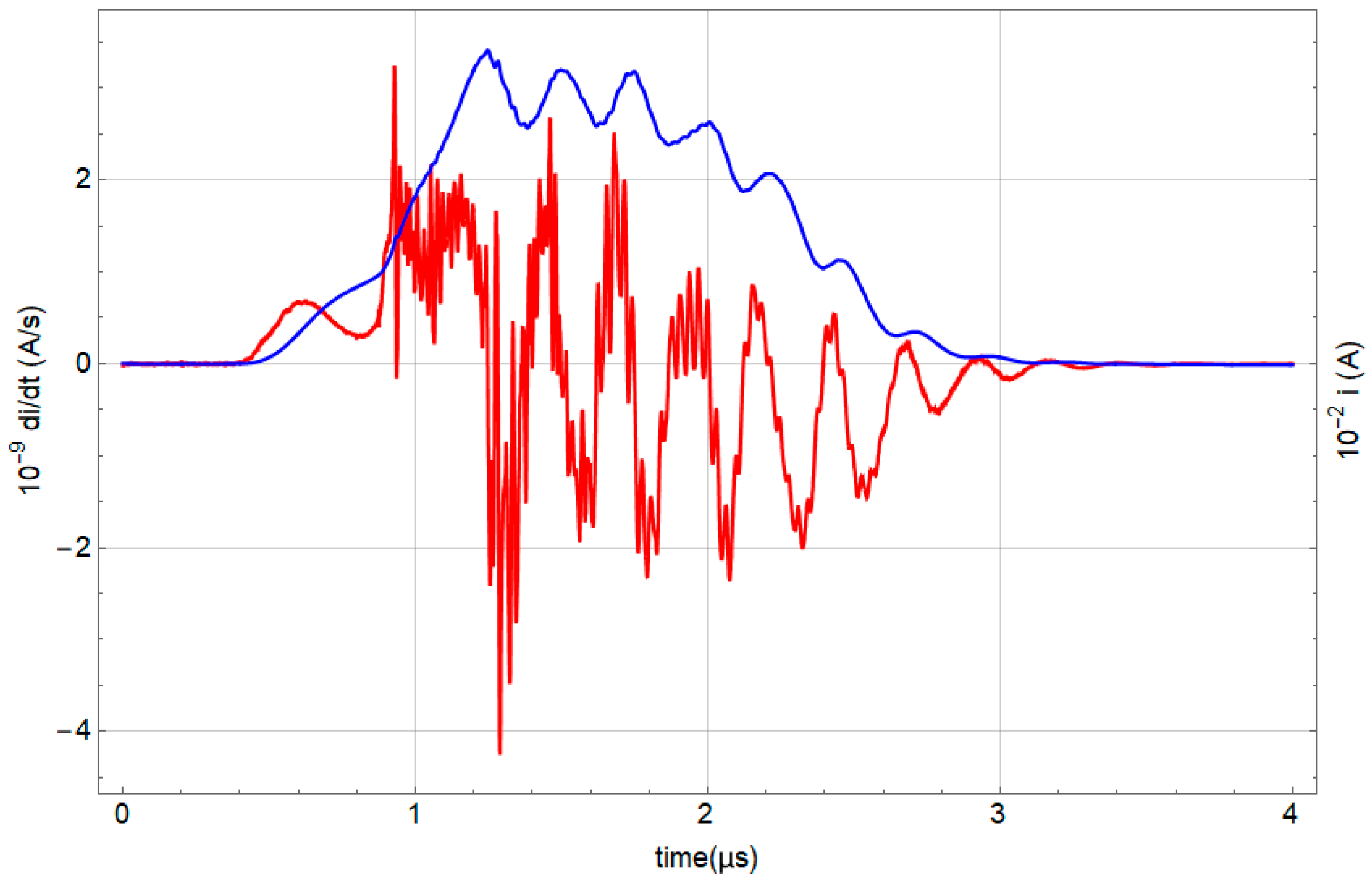
Figure 9 shows the signal obtained from the Rogowski coil at the output of the trigger unit, together with the corresponding integrated waveform representing the output current. Before spark-gap breakdown, only a few amperes flow at the trigger unit output, corresponding to the transformer’s core magnetizing current. After the breakdown, a high current begins to develop as the voltage at the spark-gap trigger electrodes is determined by the Marx Bank capacitor voltage and is limited by the series water resistors connected to the trigger electrodes. After the end of the trigger pulse and the breakdown of the spark gaps, a large current is induced at the output of the trigger unit due to the high voltage present at the spark-gap trigger electrode of the Marx Bank. This current is characterized by significant ringing. The diodes D1 and D2 at the trigger unit output protect the switching devices from these transient currents. A detailed analysis of the current waveform after spark-gap breakdown is beyond the scope of the present work, which focuses on the development and validation of the trigger generator.
The five-submodule prototype performed as expected and is currently in operation with the IPPL’s Z-Pinch machine. It is successfully replacing the thyratron-based trigger generator. It is shown that the proposed modular multilevel converter (MMC) design provides a viable approach for implementing high-voltage pulse generators capable of achieving virtually any desired output voltage by increasing the number of submodules.
5. Conclusions
This work demonstrates that the MMC topology can be effectively employed to realize a fully modular trigger generator for high-voltage pulsed-power applications. By adopting a serially propagated triggering scheme and distributed power handling across cascaded sub-modules, the proposed design achieves true modular expandability without requiring high-voltage insulation at the control stage.
The proposed trigger generator was developed to replace the previously used thyratron-based trigger unit while maintaining compatibility with the existing Marx Bank triggering system. The semiconductor implementation eliminates filament warm-up time and continuous filament power consumption while enabling a compact modular architecture.
The developed five-submodule prototype validated the proposed architecture under both laboratory and operational conditions. The system successfully generated 15 kV trigger pulses with a duration of approximately 200 ns and a measured rise time of about 100 ns while driving the primary winding of the Z-Pinch step-up transformer. The total signal propagation delay across the serially connected submodules was measured at approximately 75 ns, which is comparable to the intrinsic switching rise time of the IGBTs. Although explicit synchronization was not necessary in the current prototype, each submodule design includes a programmable delay unit enabling accurate timing alignment. Future implementations involving a larger number of cascaded modules may require a dedicated synchronization mechanism to maintain precise switching coordination and waveform integrity.
Although this work is focused on the existing transformer-coupled triggering configuration of the Z-Pinch machine, the MMC topology allows straightforward expansion by increasing the number of cascaded submodules, enabling higher output voltages and operation in repetitive mode in future implementations. Overall, the MMC topology can serve as a scalable and flexible platform for the realization of fully modular high-voltage trigger generators. The demonstrated performance establishes a foundation for future expansion toward higher-voltage and higher-current pulsed-power systems.




 ,
,