Article

Analysis of a Novel Three-Port Single-Stage Bidirectional DC–AC Converter for PV-ESS-V2G System

1
State Grid Inner Mongolia Eastern Power Co., Ltd., Hohhot 010020, China
2
College of Electrical Engineering, Zhejiang University, Hangzhou 310027, China
*
Author to whom correspondence should be addressed.
Electronics 2026, 15(7), 1360; https://doi.org/10.3390/electronics15071360
Submission received: 10 February 2026 / Revised: 18 March 2026 / Accepted: 20 March 2026 / Published: 25 March 2026

Abstract

Multiport DC–AC converters are widely used in photovoltaic-energy storage–charging systems, but traditional two-stage schemes face challenges in circuit cost and efficiency improvements. To address this issue, a novel three-port single-stage DC–AC converter is proposed for grid-connected applications. The proposed converter integrates two DC ports and one AC port through circuit multiplexing, eliminating the high-voltage DC bus and reducing system complexity. An unfolding bridge is employed at the AC port, and full bridge circuits are used at DC ports, reducing the number of high-frequency switches. The proposed single-stage topology inherently achieves galvanic isolation and bidirectional power conversion. To achieve accurate grid current regulation and wide-range zero-voltage-switching, a multiple-phase-shift modulation method is developed to ensure a sinusoidal current waveform. The effectiveness of the proposed converter and modulation method is verified through simulation results, demonstrating a peak efficiency of 97% and a total harmonic distortion of 2.91%.

1. Introduction

With the rapid growth of photovoltaic-energy storage–charging systems [1,2], such as the increasing demand for vehicle-to-grid (V2G), bidirectional power transmission technologies have attracted much interest. However, conventional schemes based on discrete converters suffer from limited efficiency, low power density, and insufficient interactions of multiple energy sources. Consequently, highly integrated multiport DC–AC converters have emerged as a promising solution [3,4]. By integrating EVs, battery energy storage, photovoltaic, and the utility grid, multiport converters enable efficient energy routing while meeting the requirements of high reliability, high power quality, and multifunctional integration in V2G applications.
Multiport high-frequency (HF) isolated DC–AC converters serve as power interfaces enabling multiport interconnection and galvanic isolation among EVs, energy storage systems, and the AC utility grid [5]. Considering the characteristics of distributed energy systems, multiport DC–AC converters are required to provide accurate bidirectional power flow control [6,7], high integration with low cost [8], high conversion efficiency [9], and galvanic isolation for safe and reliable operation [3,10,11].
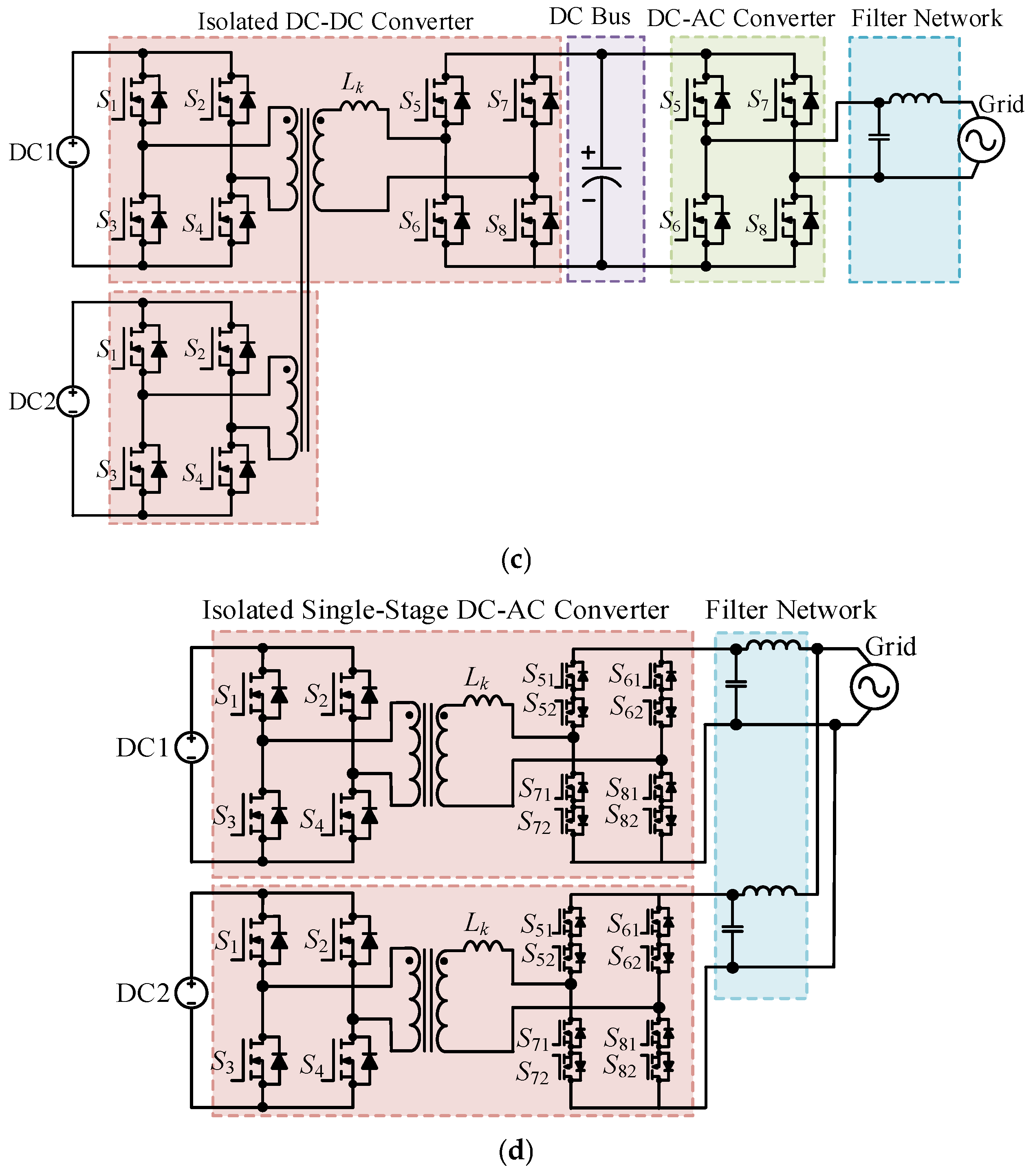
Multiport DC–AC converters can be classified into four categories according to the number of power conversion stages, including two-stage DC–AC converters with independent configuration, two-stage DC bus-coupled DC–AC converters, two-stage transformer-coupled DC–AC converters, and single-stage DC–AC converters with independent configuration.
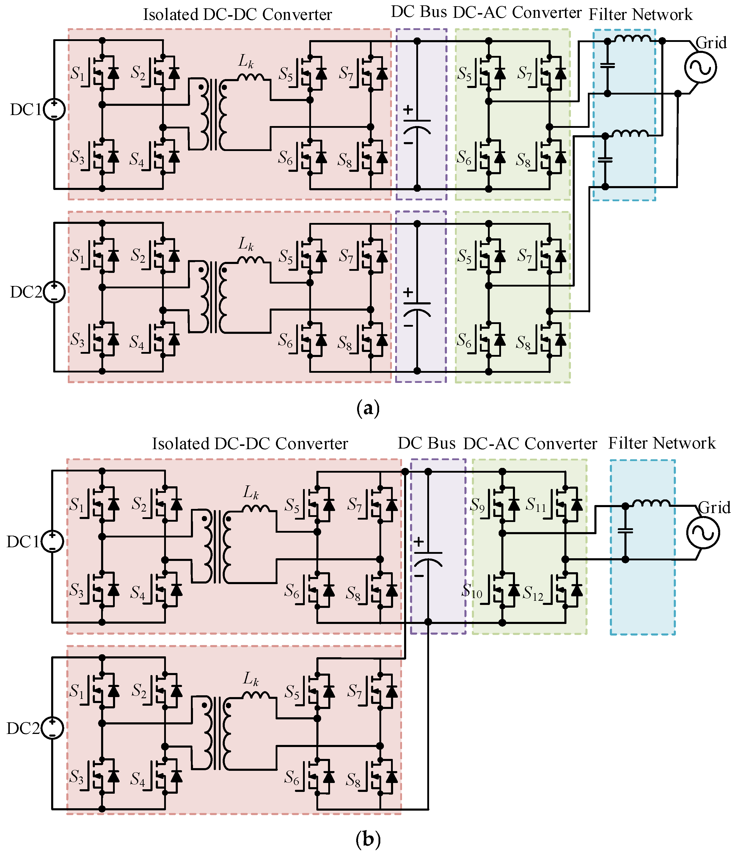
The simplified circuit of the first type is shown in Figure 1a. Each DC source employs an individual two-stage isolated DC–AC converter to achieve power conversion and interaction with the AC grid. The two-stage topology consists of a high-frequency isolated DC–DC converter, a DC bus, and a non-isolated DC–AC converter. The DC–DC converter provides buck-boost voltage regulation and galvanic isolation between the DC port and the DC bus, and the DC–AC converter regulates the grid current [12,13,14,15]. Various modulation techniques have been proposed to address common-mode voltage problems in non-isolated multilevel inverters [16]. For instance, an elimination method for three-level neutral-point-clamped (NPC) inverters was presented in [17]. However, this method focuses on non-isolated configurations and does not address the efficiency and component reduction challenges in isolated multiport systems. Since each DC source operates independently, existing isolated DC–DC and DC–AC schemes can be directly adopted. However, this structure relies on a high-voltage DC bus, which typically requires large-capacitance electrolytic capacitors for power decoupling. Although electrolytic capacitors are widely used due to their low cost, their lifespan is sensitive to environmental conditions, potentially reducing system reliability. Replacing electrolytic capacitors with film capacitors can improve power density and lifetime. Nevertheless, their high cost limits large-scale deployment [18].
Based on the first type shown in Figure 1a, the circuit structure can be simplified by sharing some specific circuit components. One approach employs individual high-frequency isolated DC–DC converters on the DC side, while sharing a single DC–AC converter for grid connection [19,20,21], as depicted in Figure 1b. Compared with the independent configuration, two DC ports are coupled through a DC bus, thereby eliminating one DC–AC conversion stage.
Compared with conventional schemes, a three-port HF isolated DC–DC converter employing a three-winding transformer enables higher integration by coupling two DC ports [22,23], as shown in Figure 1c. Overall system integration was further improved by eliminating four power switches and one magnetic core [24,25,26]. Coupling multiple DC ports via a multi-winding transformer can reduce the number of magnetic components, but this approach significantly increases transformer design complexity [19]. Moreover, the tight electromagnetic coupling between DC ports complicates the control algorithm and hinders achieving independent regulation for each port.
Recent studies have reported single-stage isolated DC–AC converters integrating isolated DC–DC and matrix-type converters [27,28], as exemplified in Figure 1d. Compared with conventional two-stage DC–AC converters, single-stage converters based on high-frequency isolated flyback, LLC resonant, and matrix-type structures can effectively eliminate the intermediate DC bus, thereby removing the bulky electrolytic capacitors and improving system reliability. However, existing studies on single-stage isolated converters primarily focus on single-port applications. When such converters are directly paralleled to accommodate multi-DC-source grid-connected applications, the total number of high-frequency switches increases substantially. Since the two single-stage DC–AC converters operate independently, further simplification through circuit multiplexing is possible.
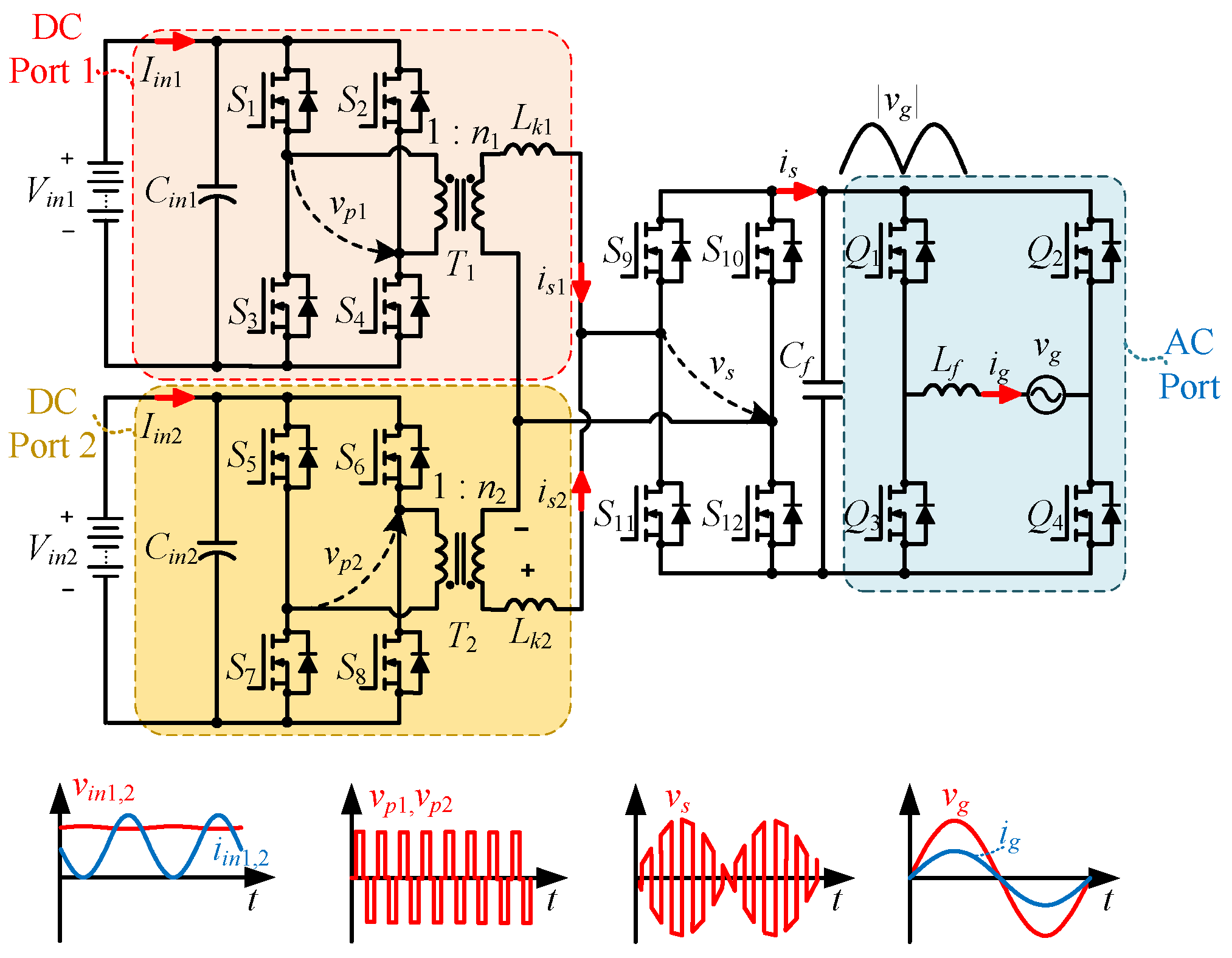
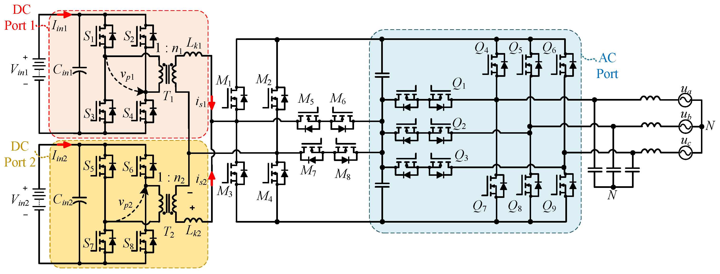
To enhance the competitiveness of multi-port converters, this paper proposes a novel three-port single-stage bidirectional DC–AC converter for PV-ESS-V2G systems. The circuit topology is shown in Figure 2. The proposed converter topology is first analyzed in detail, followed by a comprehensive explanation of its operating principles under different power flow modes. An extended phase-shift modulation strategy is then developed to achieve independent power control for each DC port while ensuring zero-voltage-switching operation across a wide load range. Simulation results validate the theoretical analysis, demonstrating a peak efficiency of 97% and a total harmonic distortion of less than 3% for the grid current.
The main contributions of this paper consist of four points. First, a novel three-port single-stage bidirectional DC–AC topology is proposed, which enables single-stage power conversion. Second, all high-frequency switches achieve zero-voltage-switching across a wide load range, resulting in a peak efficiency of 97%. Third, the proposed topology reduces the number of high-frequency switches and magnetic components by 50% compared to conventional two-stage solutions, thereby significantly reducing circuit cost and volume. Fourth, an extended phase-shift control strategy is introduced to achieve independent control for each DC port.
This paper is organized as follows. The operation principle of the proposed converter is shown in Section 2. Simulation results are shown in Section 3. Section 4 discusses the losses, total harmonic distortion, comparison studies, and the application prospects in three-phase applications. Section 5 concludes the paper.

2. Operation Principle

2.1. Overview of the Proposed Topology

Figure 2 shows the circuit diagram of the proposed three-port single-stage bidirectional DC–AC converter. It features two DC ports and one grid connection interface, enabling the integration of various energy sources such as photovoltaics, energy storage, and electric vehicles, and facilitating single-stage power conversion and multi-mode interaction with the grid. The DC-side bridges of Port 1 and Port 2 are both full bridge circuits with four HF switches S1S4 and S5S8. The midpoint of the full bridge, denoted as vp1 or vp2, is connected to a transformer to form an independent port. The turn ratios of transformers T1 and T2 are denoted as n1 and n2, and leakage inductors are lumped in the secondary as Lk1 and Lk2, respectively. Subsequently, the outputs of Port 1 and Port 2 are connected in parallel to the grid-side bridge, which consists of switches S9S12. The secondary midpoint voltage vs. is clamped by the utility grid. Lf and Cf form an L-C filter to bypass the high-frequency component of is and generate the grid current ig. An unfolding-bridge circuit is used to reverse the polarity of grid voltage vg and current ig, which consists of Q1~Q4.
During the positive half cycle of the grid voltage, switches Q1 and Q4 are turned on. During the negative cycle of the grid voltage, the switches Q2 and Q3 are turned on. To simplify the analysis, we assume that each component is ideal in steady state and the converter is lossless, meaning Vin × Iin = vg × ig. The switching frequency fs is much higher than the line frequency fg. Assume that the grid voltage vg is a pure sinusoidal waveform as
v g = V g sin ( θ g )
where Vg and θg represent the peak value and phase angle of grid voltage, respectively.
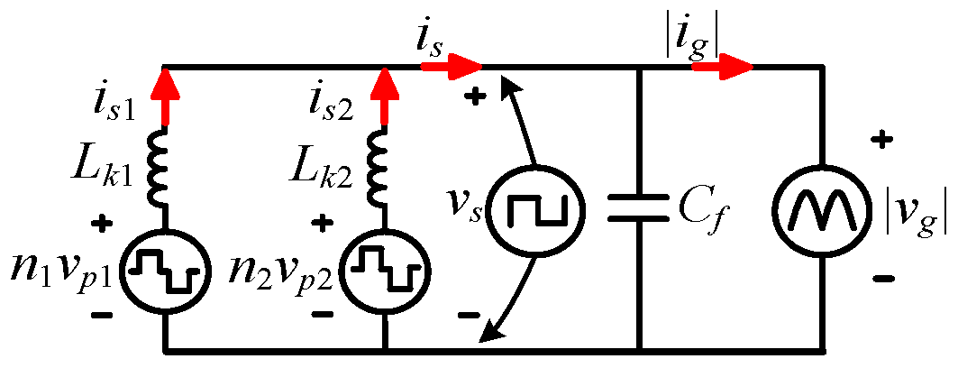
Figure 3 shows the equivalent circuit of the proposed three-port converter. It is noted that the waveforms of vp1, vp2, and vs. can be controlled independently. Therefore, the currents is1, is2, and is can be controlled independently by adjusting the internal phase-angle α1, α2 of vp1 and vp2 and the external phase-angle β1, β2 between vp1, vp2, and vs.
The switches S9S12 operate at a high frequency to generate a high-frequency voltage vs. at the secondary midpoint. This full bridge generates high-frequency AC current, which, after being filtered by the filter network Lf-Cf, results in a pulsating DC current with double line frequency. The unfolding bridge (Q1Q4) operates at line frequency and converts the pulsating DC current into a sinusoidal AC current.
The proposed converter supports bidirectional power transmission for each DC port independently. When power is delivered from the DC Port 1 to the AC grid, the primary-side full bridge generates a high-frequency voltage with a leading phase β1 relative to vs. As a result, energy flows from the DC source to the grid. Conversely, when power is absorbed from the grid into a DC port, the primary-side voltage lags behind vs, indicating reverse power flow. This phase-shift control strategy allows each DC port to operate in either discharging mode (DC to AC) or charging mode (AC to DC) independently, enabling flexible power management in multi-source applications, such as simultaneous EV charging and discharging, or mixed renewable generation and storage coordination.

2.2. Modulation for Power Transmission from DC Port to AC Port

A modulation strategy based on extended phase shift (EPS) is introduced for precise control. Because of the independence of each DC port, Port 1 is selected as an example.
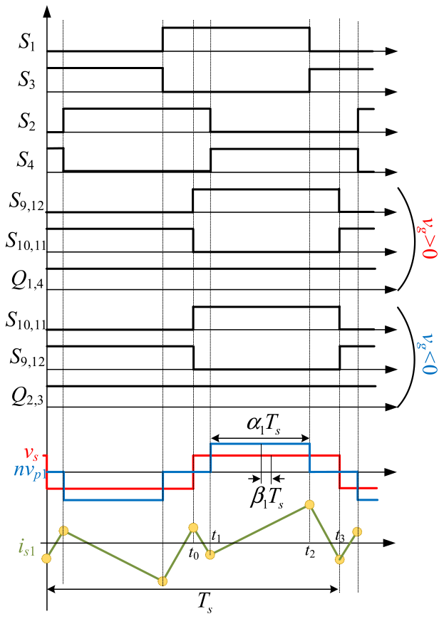
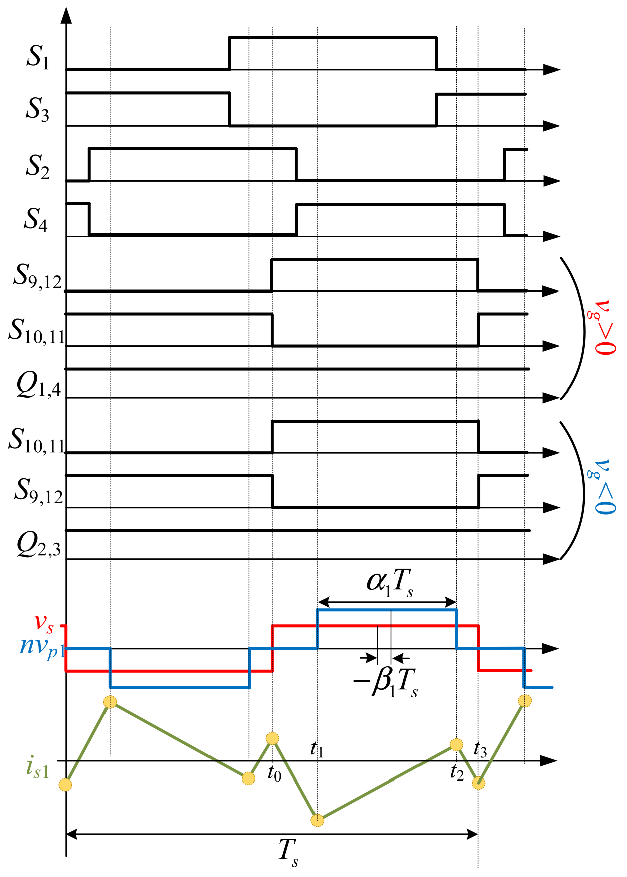
Figure 4 shows the theoretical waveforms of primary midpoint voltage n1 × vp1, secondary midpoint voltage vs, and secondary current is1. The three-level voltage vp1 switches between Vin1, zero, and −Vin1 with a pulse width of α1Ts. The two-level voltage vs. pulsates from |vg| to −|vg| with a pulse width of 0.5Ts. The phase-shift angle β1 is defined as the leading time ratio between the center of vp1 and the center of vs. In this mode, the span of the primary voltage vp1 is within the secondary voltage vs. Therefore, the phase-shift angle β1 is given by
β 1 > 0.25 0.5 α 1
The slopes of the transformer current is1 in each interval can be derived as
d i s 1 d t = v g / L k 1 ,   ( t 0 , t 1 ) , ( t 2 , t 3 ) n 1 V i n 1 v g / L k 1 ,   ( t 1 , t 2 )  
In addition, the current waveforms during a half switching period are symmetric along the t-axis, implying that is1(t0) equals −is1(t3). From this relationship and (3), is1(t0) is obtained as
i s 1 ( t 0 ) = T s 2 L k 1 0.5 v g α 1 n 1 V i n 1
Using (3) and (4), the average output current ig1 generated by Port 1 is derived as
i g 1 = 1 T s t 0 t 3 i s 1 ( τ ) d τ = n 1 V i n 1 L k 1 f s α 1 β 1
Equation (5) shows that the relation between control variables α1, β1, and the average output current ig1 is linear, so the output power can be precisely controlled by adjusting their amplitudes. To simplify the controller structure and obtain a sinusoidal grid-connected current, the phase-shift angle α1 can be given as
α 1 ( θ g ) = α 1 m sin θ g .
where α1m is the peak value of α1. By substituting (6) into (5), the average output current ig1 can be rewritten as
i g 1 = n 1 V i n 1 L k 1 f s β 1 α 1 m sin θ g .
From (7), it can be seen that a sinusoidal grid-connected current can be obtained by modulating the phase shift angle α1 according to the sine law. In addition, the amplitude β1 can be calculated based on the power reference value, expressed as
β 1 = 2 P r e f n 1 V i n 1 L k 1 f s α 1 m V g .
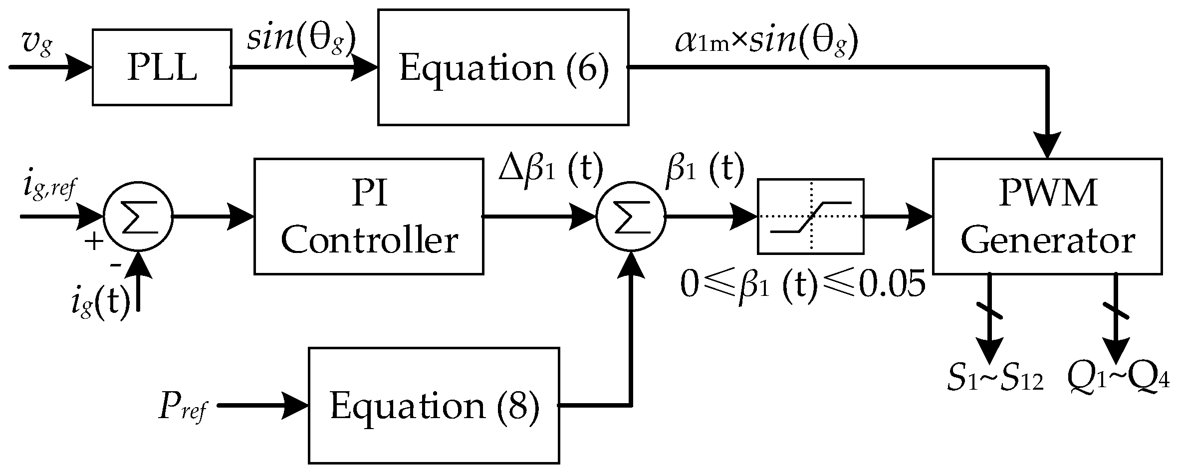
The control block diagram of the proposed solution is shown in Figure 5. The external power reference command comes from the battery management system or the charging control module. Since the focus of this paper is on the bidirectional power transmission function, the specific charging strategy is not presented. The power reference value is calculated using formula (8) to obtain the corresponding phase shift angle amplitude, and then the drive signal is obtained by modulating the phase shift angle according to (6). To achieve precise power control, a current loop was added to track the grid-connected current.
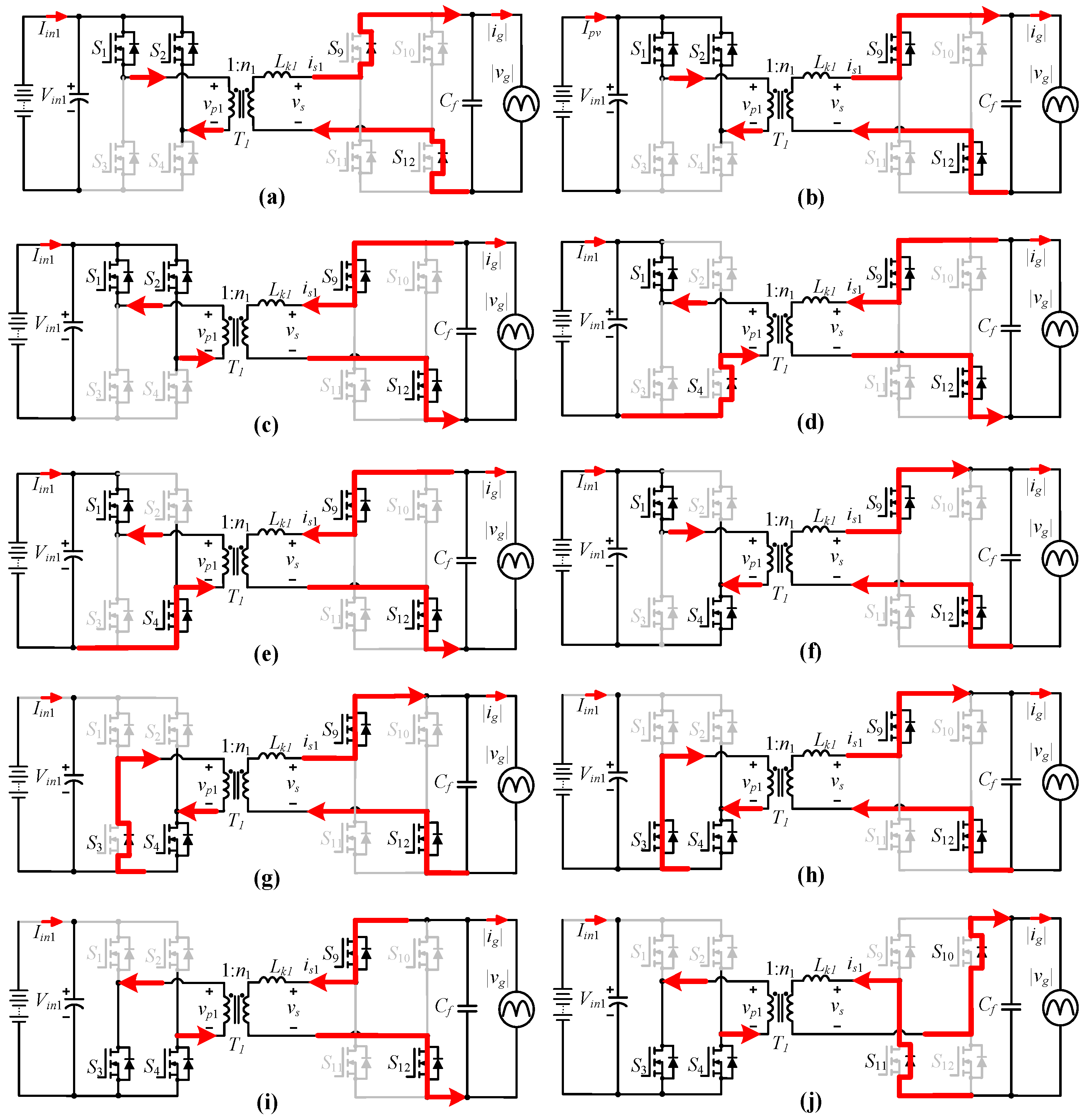
The switching-frequency fs in (5) is designed as a constant (CSF) of 50 kHz. Using the control law (6), the power flows of DC Port 1 and DC Port 2 can be precisely controlled. Figure 6 shows the circuit transients from t0 to t3, consisting of ten operating stages. At Stage 1, Stage 4, and Stage 7, all of the switches S1S4 and S9S12 have achieved ZVS, which ensures the high efficiency of the proposed topology.
Stage 1: t = t0. S3, S4, S9–S12 are turned off; S1 and S2 are turned on. The leakage current flows through the body diodes of S9 and S12, thereby fully discharging the parasitic capacitance. This leads to ZVS turn-on of S9 and S12.
Stage 2: t0 < t < t1 & is1 > 0. S3, S4, S10–S11 are turned off; S1, S2, S9, and S12 are turned on.
Stage 3: t0 < t < t1 & is1 < 0. Being similar to Stage 2, S3, S4, S10–S11 are turned off; S1, S2, S9, and S12 are turned on.
Stage 4: t = t1. S2, S3, S4, S10–S11 are turned off; S1, S9, and S12 are turned on. The leakage current flows through the body diodes of S4, thereby fully discharging the parasitic capacitance. This leads to ZVS turn-on of S4.
Stage 5: t1 < t < t2 & is1 < 0. S2, S3, S10–S11 are turned off; S1, S4, S9, and S12 are turned on. The primary current flows in the opposite direction.
Stage 6: t1 < t < t2 & is1 > 0. S2, S3, S10–S11 are turned off; S1, S4, S9, and S12 are turned on. The primary current is flowing in the forward direction.
Stage 7: t = t2. S1, S2, S3, S10–S11 are turned off; S4, S9, and S12 are turned on. The leakage current flows through the body diodes of S3, thereby fully discharging the parasitic capacitance. This leads to ZVS turn-on of S3.
Stage 8: t2 < t < t3, is1 > 0. S1, S2, S10–S11 are turned off; S3, S4, S9, and S12 are turned on. The secondary current is flowing in the forward direction.
Stage 9: t2 < t < t3, is1 < 0. S1, S2, S10–S11 are turned off; S3, S4, S9, and S12 are turned on. The secondary current is flowing in the opposite direction.
Stage 10: t = t3. S1, S2, S9–S12 are turned off; S3 and S4 are turned on. The leakage current flows through the body diodes of S10 and S11, thereby fully discharging the parasitic capacitance. This leads to ZVS turn-on of S10 and S11.

2.3. Modulation for Power Transmission from AC Port to DC Port

The operation principle of AC to DC power delivery is similar to that of the DC–AC mode, but the geometric center of the voltage vp1 lags behind vs, as shown in Figure 7. The negative sign of β1 indicates the lagging angle. Therefore, the average input current ig1 for Port 1 is derived as
i g 1 = 1 T s t 0 t 3 i s 1 ( τ ) d τ = n 1 V i n 1 L k 1 f s α 1 β 1
The negative sign of ig1 in (9) indicates that power flows from the AC grid to DC Port 1. Therefore, bidirectional power control is achievable, and the proposed control strategy enables independent bidirectional power regulation for all ports.

2.4. Analysis of ZVS Constraint

The ZVS condition for the primary switches is determined by the polarity and magnitude of the transformer current at the switching instant. Taking the switches S1–S4 of Port 1 as an example, to achieve zero-voltage turn-on for S1 and S4, the current is1(t0) must be negative to discharge the output capacitances of the switches before turn-on. For S2 and S3, ZVS requires that is1(t3) be positive.
i s 1 ( t 0 ) = T s 2 L k 1 0.5 v g α 1 n 1 V i n 1 < 0
From Equation (10), it can be observed that as long as the external phase-shift angle β1 is properly selected within its feasible range, is1(t0) maintains a sufficient negative value to ensure ZVS operation for S1 and S4, while the positive amplitude of is1(t3) is also adequate to complete the discharge of the output capacitances of S2 and S3.
For the primary switches S5–S8 of Port 2, the ZVS condition is completely symmetric to that of Port 1. Specifically, to achieve ZVS for S5 and S8, the current is2(t0) must be negative. For S6 and S7, ZVS requires that is2(t3) be positive. Due to the circuit symmetry and the consistency of the modulation strategy, when the external phase-shift angle β2 is selected within a reasonable range, is2(t0) maintains a sufficient negative value to ensure zero-voltage turn-on for S5 and S8, while the positive amplitude of is2(t3) is also adequate to complete the discharge of the output capacitances of S6 and S7.
In practical implementation, these non-idealities, including parasitic components and timing constraints, have an impact on system efficiency. Among them, two critical factors significantly affect switching losses: the switch’s parasitic output capacitance and the effect of the dead-time interval of high-frequency switches.
First, while ZVS aims to discharge the junction capacitance before turn-on, the non-linear and voltage-dependent characteristic of the parasitic capacitance complicates this process. If the energy stored in the parasitic capacitance is not completely discharged by the leakage current during the switching transition, it leads to additional dissipation. Therefore, the improved ZVS constraints can be expressed as
i s 1 ( t 0 ) u d c × C o s s / L k 1
Second, the dead-time must be long enough to allow the leakage current to fully charge or discharge the parasitic capacitances. If the dead-time is too short, the transition is incomplete, resulting in hard-switching. Conversely, if the dead-time is excessive, it can lead to body diode conduction, which causes reverse recovery losses and increased conduction losses due to the diode’s relatively high forward voltage drop. Therefore, optimizing the dead-time is crucial for maintaining high efficiency in practical applications.

2.5. Design of Leakage Inductance

The proposed topology relies on a single inductor, i.e., the leakage inductance, to perform high-frequency power conversion. Therefore, the core of the circuit parameter design lies in the leakage inductance design. According to (7), when the input voltage and the switching frequency are determined, the leakage inductance determines the maximum output power of the circuit. Given that the voltage variation range of 400 V-level electric vehicles is 300–450 V, and the corresponding SOC is 20–100%, the inductance value should be designed based on the lowest DC voltage, as this represents the worst working condition and the maximum current stress.
L k 1 n 1 V i n 1 β 1 , max V g α 1 m 2 P o , max f s
where Po,max is the maximum output power. The amplitude of the inner phase shift angle is α1m = 0.35. Substituting parameter values, including n1 = 1, Vin1 = 400 V, β1,max = 0.05, Vg = 220, Po,max = 6600, and fs = 50 kHz, into (12), the leakage inductance is designed as 3.29 μH.

3. Simulation Results

This paper develops a simulation model of a three-port single-stage DC–AC converter using the PLECS version 4.8.9 platform. The simulation model is developed and analyzed using the PLECS platform, which is well-suited for power electronic simulations due to its fast simulation speed and robust handling of switched systems.
To improve the accuracy of the model and better reflect real-world performance, practical parasitic parameters are included in the device models. The MOSFETs are modeled with a specified on-resistance to represent conduction losses, and parasitic inductances are added at the leads to account for switching transients and voltage ringing. Similarly, the diodes are modeled with their on-resistance and forward voltage drop.
This simulation platform supports the import of the actual parameters of power devices into the model. For instance, we imported the parameters of Infineon’s 650 V MOSFET, which are usually obtained from the data sheets provided by the manufacturer. This enables the simulation platform to conduct loss simulation and thermal simulation. These functions ensure that the simulation results more closely match the behavior of an actual hardware prototype.
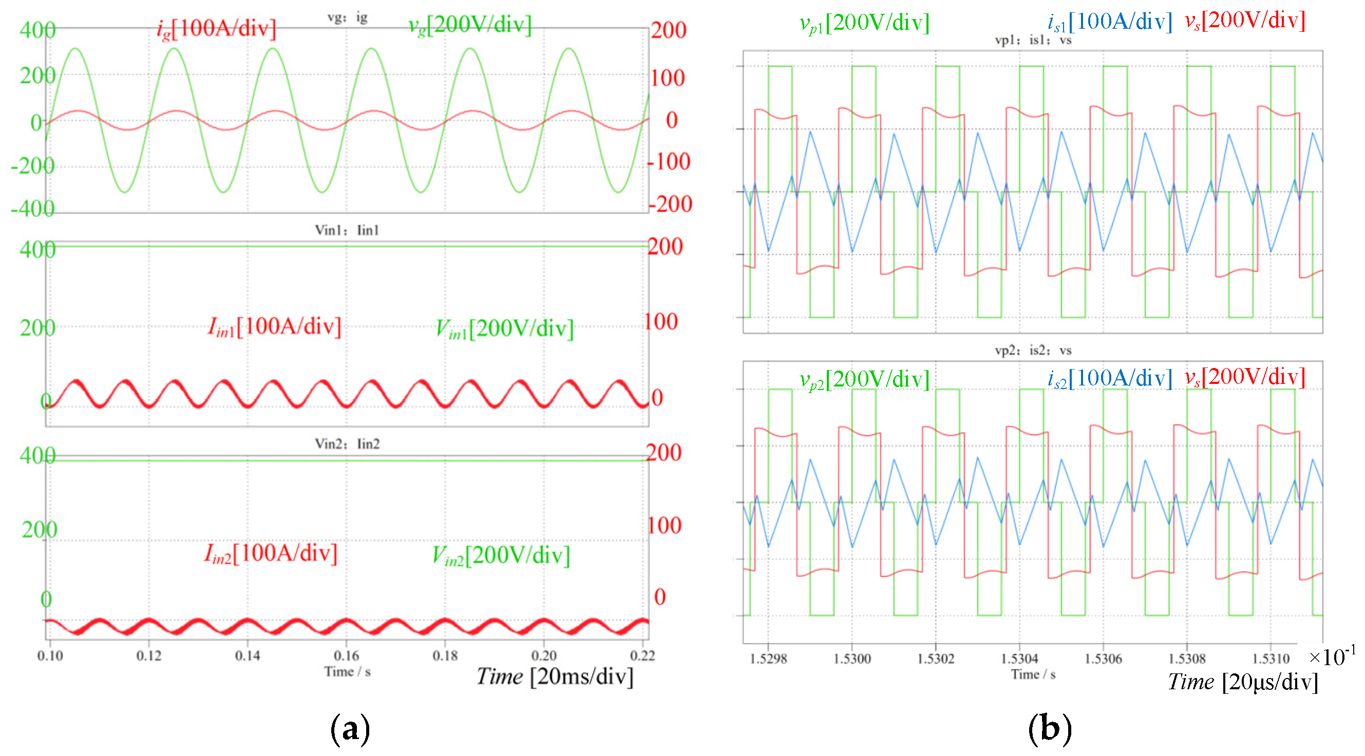
The circuit parameters are listed in Table 1. To evaluate its performance in EV grid-connection applications, the two DC ports are assumed to be connected to two EVs. Under this assumption, four representative operating conditions are defined: (1) both DC Ports 1 and 2 deliver power to the utility grid, (2) both DC ports operate in charging mode and draw power from the grid, (3) DC Port 1 delivers power to the grid while DC Port 2 operates in charging mode, (4) both DC ports operate at rated power in the discharging mode and deliver power to the grid.
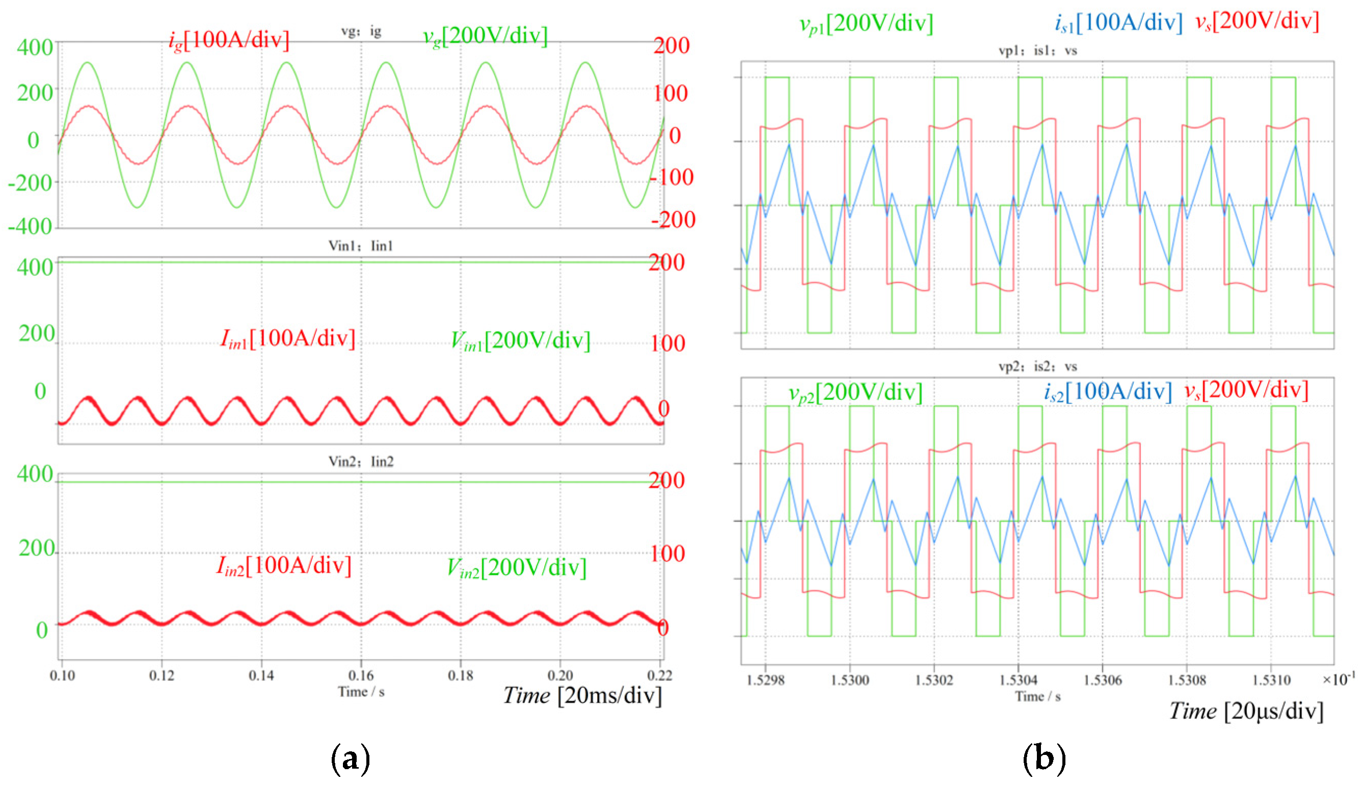
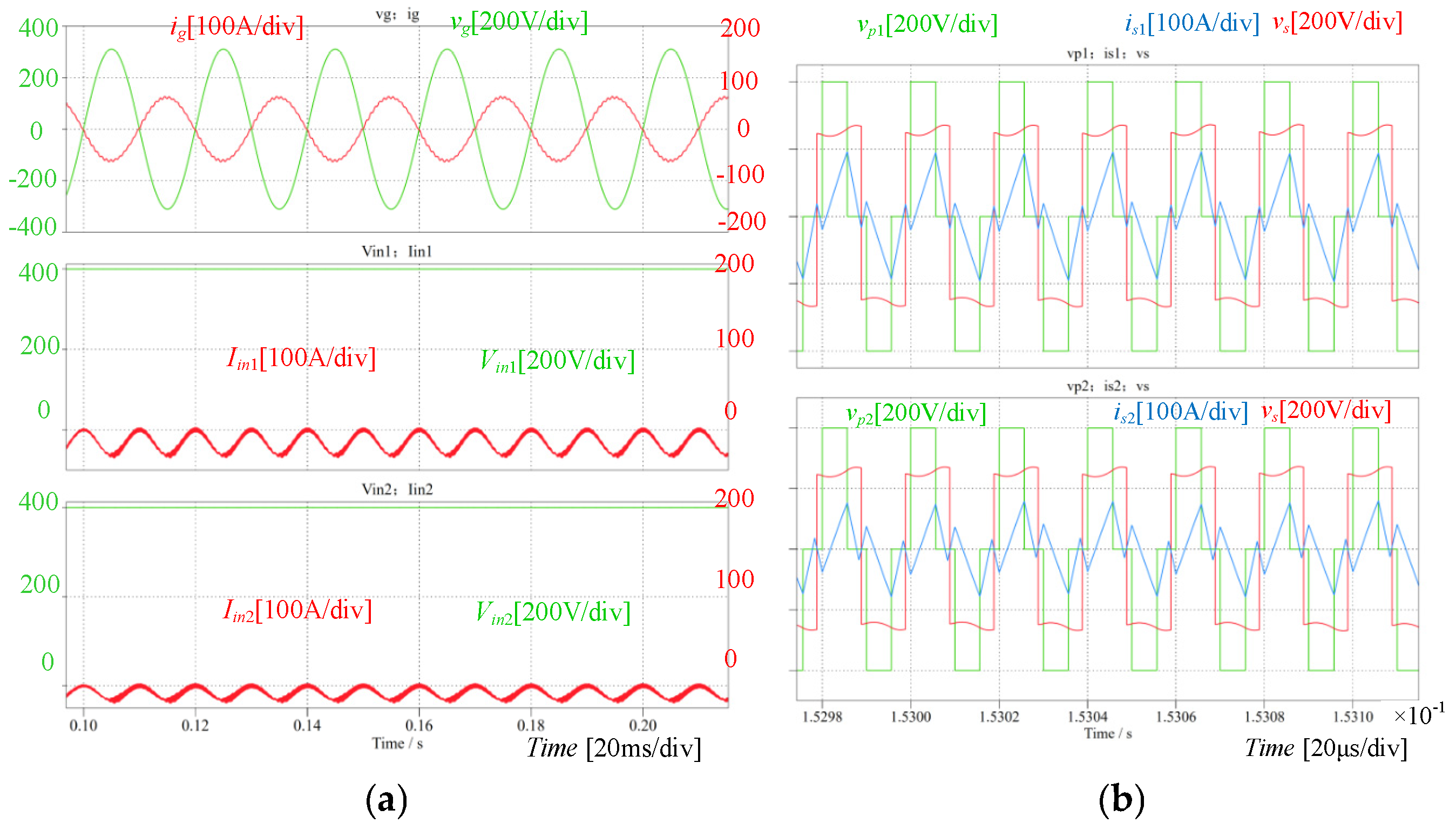
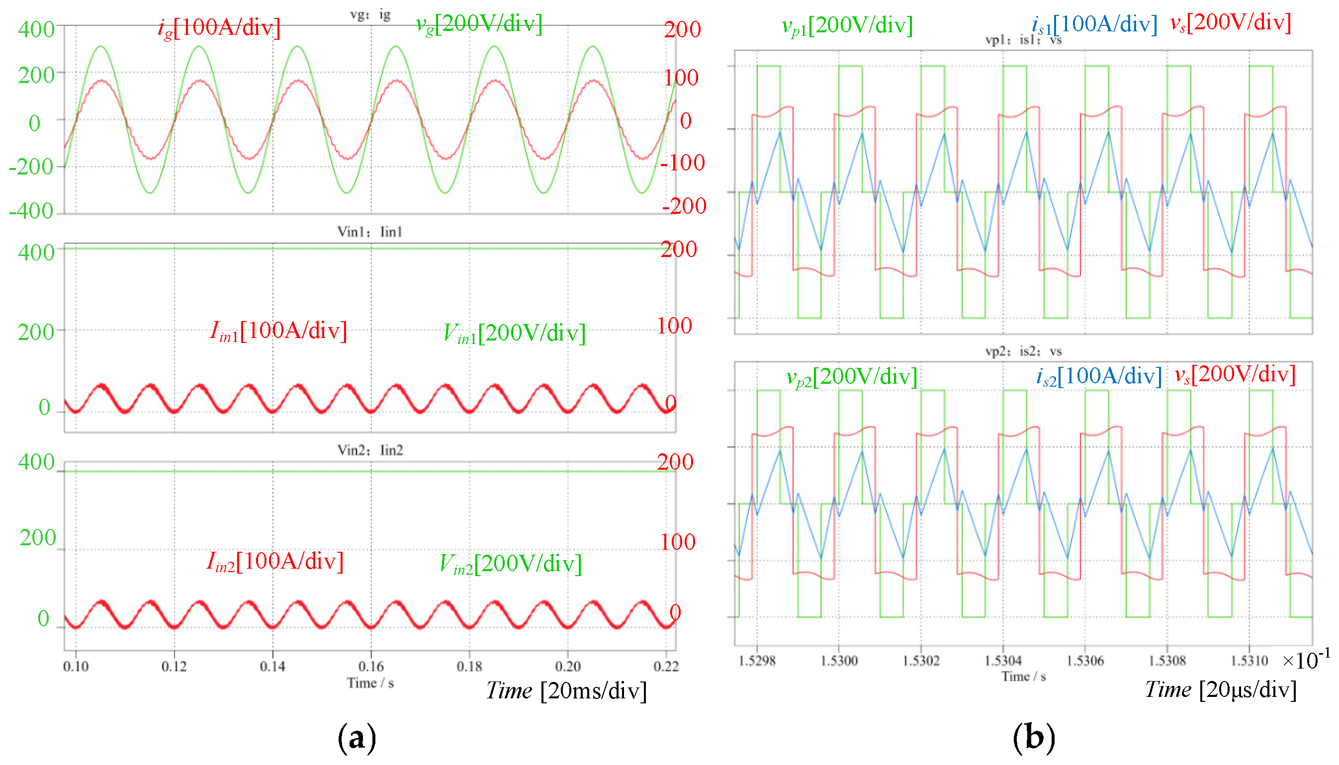
Correspondingly, four simulation cases are established and verified. Case 1 represents the simultaneous discharging of two EVs into the grid, with the output power set to 6.6 kW at DC Port 1 and 3.3 kW at DC Port 2, as shown in Figure 8. Case 2 corresponds to the simultaneous charging of both EVs from the grid, where the charging power is 6.6 kW at DC Port 1 and 3.3 kW at DC Port 2, as shown in Figure 9. Case 3 illustrates a mixed operating condition in which one EV discharges to the grid while the other is in the charging mode. In this case, DC Port 1 delivers 6.6 kW to the grid, whereas DC Port 2 draws 3.3 kW, as shown in Figure 10. Case 4 corresponds to the simultaneous charging of both EVs from the grid, where the charging power is 6.6 kW at both DC ports, as shown in Figure 11.
The summary of the total harmonic distortion (THD) of the grid-connected current for the proposed topology is shown in Table 2. The THD of the grid-connected current at the rated output power is 2.91%, which is less than 3%. The simulation results show that the proposed three-port single-stage DC–AC converter can achieve precise power control and bidirectional power transmission.
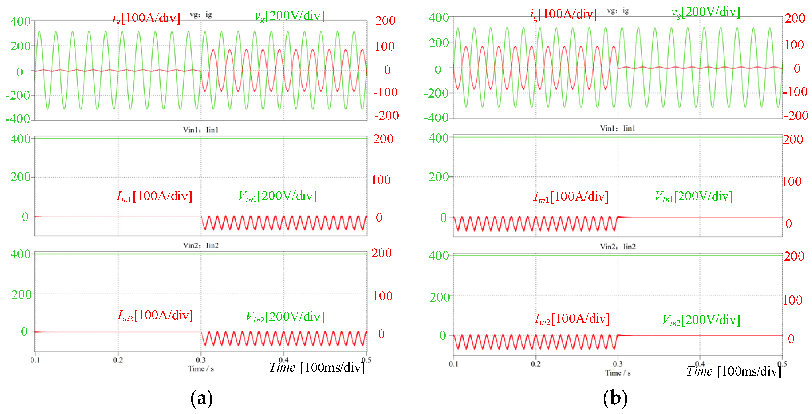
Figure 12 presents the dynamic response curve of the grid-connected current. Figure 12a shows the response curve of the output power when it steps from 0 to 6.6 kW, and Figure 12b shows the response curve when the output power decreases from 6.6 to 0 kW. The proposed topology can enter a new steady state within half of a power frequency cycle, demonstrating excellent dynamic response speed.

4. Discussion

4.1. Analysis of Power Loss

The loss of the proposed converter includes conduction loss, switching loss, and core loss. The conduction loss can be divided into the conduction loss of the unfolding bridge Pc_ufd, and the conduction loss of the high-frequency switches Pc_dab. Pc_ufd can be expressed as
P c _ u f d = I g 2 2 R d s _ u f d
where Ig is the rms grid current, and Rds_ufd is the on-resistance of the unfolding bridge switches.
P c _ dab = ( 1 + n 1 2 ) I s 1 2 2 R o n + ( 1 + n 2 2 ) I s 2 2 2 R o n
where Is1 and Is2 are the rms values of currents is1 and is2, n1 and n2 are the transformer turns ratio, and Ron is the on-resistance of the high-frequency switches.
The switching loss consists of turn-off loss Ps_off and turn-on loss Ps_on. The turn-on loss expression of one switch is expressed as
P s _ o n S x = C o s s U d s 2 2 T s
where Uds is the drain–source voltage. The turn-off loss expression of one switch is evaluated as
P s _ o f f S x = U d s I d 2 T s Q g d + Q g s Q t h U plat / R G o f f
where Uplat is the voltage at the Miller platform. RG is the gate resistance. Qgd, Qgs, and Qth are the charges of the different stages, which can be obtained from the datasheet of the switch.
The core loss of the transformer is calculated by the improved generalized Steinmetz equation.
P Core = V e 1 T s 0 T s k i | d B d t | α ( Δ B ) β α d t k i = k 2 π α 1 0 2 π cos θ α 2 β α d θ
dB/dt is the gradient of the magnetic flux density. ΔB is the peak-to-peak flux density. Ve is the volume of the core. k, α, and β are the parameters of the Steinmetz equation. The copper loss of the transformer can be expressed as
P cu = I s 1 2 R c u 1 , s + n 1 2 I s 1 2 R c u 1 , p + I s 2 2 R c u 2 , s + n 2 2 I s 2 2 R c u 2 , p
The average value of the total power losses, Ploss, can be obtained by integrating these loss components over half a line cycle.
P l o s s = 1 π 0 π ( P c _ u f d + P c _ dab + 4 P s _ o n + 4 P s _ o f f + P c o r e + P cu ) d θ
Based on (19), the calculated conversion efficiencies under different output powers are summarized in Table 3. The detailed distribution of losses is shown in Table 4. Under heavy-load conditions, the main loss comes from conduction loss.

4.2. Grid Current’s THD

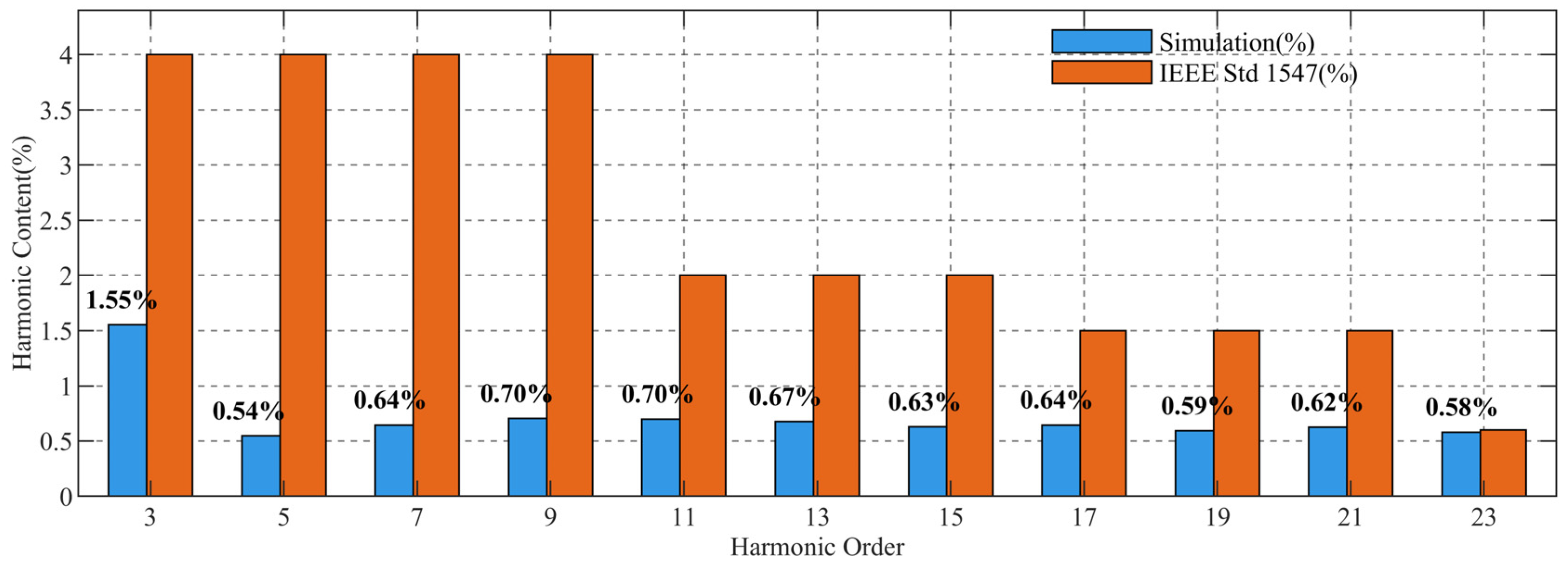
Based on the PLECS simulation platform, we can obtain the total harmonic distortion of the grid-connected current at the rated power as well as the amplitudes of each harmonic component. These data are obtained through the FET tool and shown in Figure 13. By comparing with the IEEE std 1547, it can be seen that the harmonics injected by the proposed converter meet the standard requirements and have a large margin.

4.3. Comparison Studies

This section compares the proposed scheme with those of the four existing schemes in terms of the high-frequency switches, inductors, capacitors, high voltage DC-link, and control strategies, as shown in Table 5. Compared with the existing solutions, the proposed topology has a significant advantage in terms of the number of high-frequency switches, reduced by up to 50%. Moreover, additional boost inductors and bulky, large-capacity capacitors are eliminated. This makes the proposed scheme a promising solution in terms of cost and power density.

4.4. Application Prospects

The proposed three-port single-stage DC–AC converter exhibits promising potential for further extension to both single-phase DC and three-phase AC applications. The modular design and flexible power flow control inherent in the topology allow for straightforward transplantation.
Regarding extension to single-phase DC systems, such as DC microgrids or DC-coupled EV charging stations, the proposed topology can be adapted by eliminating the grid-side inverter stage and directly interfacing the DC ports with a common DC bus. This would simplify the control structure and reduce conversion stages, potentially improving overall efficiency. In addition, further research is also required to address the control complexity, component sizing, and system-level integration for extended topologies.
For three-phase AC grid integration, the proposed single-phase structure can be extended to form a three-phase system, enabling higher power transfer capability, such as active and reactive power control. For instance, the secondary circuit can be replaced by a T-type converter and a Swiss converter to interface the three-phase utility grid. The extended circuit topology for three-phase grid-connected applications is shown in Figure 14. Being similar to the unfolding bridge, the Swiss converter operates at low frequency. However, this extension introduces challenges in terms of increased component count and more complex control algorithms.

5. Conclusions

This paper presents a three-port single-stage DC–AC converter for photovoltaic energy storage–charging systems. Compared with conventional two-stage multiport topologies, the number of high-frequency switches is reduced by 50%, leading to lower circuit complexity and cost. By coupling multiple DC sources through sub-transformers, the proposed topology achieves single-stage power conversion, decoupling control, and high expansion flexibility. To satisfy the flexible bidirectional power interaction requirements between the grid and multiple sources, an EPS-based modulation strategy is proposed, thereby enabling independent and precise power control of each port. Simulation results under multiple operating conditions confirm that the proposed topology achieves precise current control and bidirectional power transmission, demonstrating its suitability for integrated multiport power conversion applications.

Author Contributions

Conceptualization, C.L.; Methodology, F.Z.; Validation, H.C.; Formal analysis, Y.B.; Investigation, D.W. and W.M.; Writing—original draft, C.D.; Writing—review & editing, F.J.; Supervision, M.C.; Project administration, M.C. All authors have read and agreed to the published version of the manuscript.

Funding

This research was supported by the State Grid Inner Mongolia Eastern Power Company Technology Project (Project No. SGMDDK00DJJS2400189).

Data Availability Statement

The original contributions presented in this study are included in the article. Further inquiries can be directed to the corresponding author.

Conflicts of Interest

Author Chunhui Liu, Yinfu Bao, Da Wang, Haoran Chen were employed by the company State Grid Inner Mongolia Eastern Power Co., Ltd. The remaining authors declare that the research was conducted in the absence of any commercial or financial relationships that could be construed as a potential conflict of interest.

References

  1. Babu, T.S.; Vasudevan, K.R.; Ramachandaramurthy, V.K.; Sani, S.B.; Chemud, S.; Lajim, R.M. A Comprehensive Review of Hybrid Energy Storage Systems: Converter Topologies, Control Strategies and Future Prospects. IEEE Access 2020, 8, 148702–148721. [Google Scholar] [CrossRef]
  2. Cao, J.; Emadi, A. A New Battery/UltraCapacitor Hybrid Energy Storage System for Electric, Hybrid, and Plug-In Hybrid Electric Vehicles. IEEE Trans. Power Electron. 2012, 27, 122–132. [Google Scholar]
  3. Zhao, S.; Li, Q.; Lee, F.C.; Li, B. High-Frequency Transformer Design for Modular Power Conversion From Medium-Voltage AC to 400 VDC. IEEE Trans. Power Electron. 2017, 33, 7545–7557. [Google Scholar]
  4. Chen, T.; Yu, R.; Huang, A.Q. Variable-Switching-Frequency Single-Stage Bidirectional GaN AC–DC Converter for the Grid-Tied Battery Energy Storage System. IEEE Trans. Ind. Electron. 2022, 69, 10776–10786. [Google Scholar]
  5. Ahmad, A.; Qin, Z.; Wijekoon, T.; Bauer, P. An Overview on Medium Voltage Grid Integration of Ultra-Fast Charging Stations: Current Status and Future Trends. IEEE Open J. Ind. Electron. Soc. 2022, 3, 420–447. [Google Scholar] [CrossRef]
  6. Gautam, A.R.; Gourav, K.; Guerrero, J.M.; Fulwani, D.M. Ripple Mitigation With Improved Line-Load Transients Response in a Two-Stage DC–DC–AC Converter: Adaptive SMC Approach. IEEE Trans. Ind. Electron. 2018, 65, 3125–3135. [Google Scholar] [CrossRef]
  7. IEEE Std 1547-2018; IEEE Standard for Interconnection and Interoperability of Distributed Energy Resources with Associated Electric Power Systems Interfaces. (Revision of IEEE Std 1547-2003); IEEE: New York, NY, USA, 2018; pp. 1–138.
  8. Jain, P.; Pahlevaninezhad, M.; Pan, S.; Drobnik, J. A Review of High-Frequency Power Distribution Systems: For Space, Telecommunication, and Computer Applications. IEEE Trans. Power Electron. 2014, 29, 3852–3863. [Google Scholar] [CrossRef]
  9. Lawder, M.T.; Suthar, B.; Northrop, P.W.C.; De, S.; Hoff, C.M.; Leitermann, O.; Crow, M.L.; Santhanagopalan, S.; Subramanian, V.R. Battery Energy Storage System (BESS) and Battery Management System (BMS) for Grid-Scale Applications. Proc. IEEE 2014, 102, 1014–1030. [Google Scholar] [CrossRef]
  10. Ronan, E.R.; Sudhoff, S.D.; Glover, S.F.; Galloway, D.L. A Power Electronic-Based Distribution Transformer. IEEE Trans. Power Deliv. 2002, 17, 537–543. [Google Scholar] [CrossRef]
  11. She, X.; Huang, A.Q.; Burgos, R. Review of Solid-State Transformer Technologies and Their Application in Power Distribution Systems. IEEE J. Emerg. Sel. Top. Power Electron. 2013, 1, 186–198. [Google Scholar] [CrossRef]
  12. Li, C.; Liu, J.; Du, S.; Dang, H.; Deng, Z.; Chen, H. A T-Type DAB-Based Isolated DC-DC-AC Three-Port Converter With High Power Efficiency. IEEE Trans. Power Electron. 2023, 38, 14178–14194. [Google Scholar] [CrossRef]
  13. Sayed, M.A.; Suzuki, K.; Takeshita, T.; Kitagawa, W. PWM Switching Technique for Three-Phase Bidirectional Grid-Tie DC–AC–AC Converter With High-Frequency Isolation. IEEE Trans. Power Electron. 2018, 33, 845–858. [Google Scholar]
  14. Kadam, A.H.; Williamson, S.S. A Common DC-Bus-Configured Traction Motor Emulator Using a Virtually Isolated Three-Phase AC-DC Bidirectional Converter. IEEE Access 2021, 9, 80621–80631. [Google Scholar]
  15. Kacetl, J.; Fang, J.; Kacetl, T.; Tashakor, N.; Goetz, S. Design and Analysis of Modular Multilevel Reconfigurable Battery Converters for Variable Bus Voltage Powertrains. IEEE Trans. Power Electron. 2023, 38, 130–142. [Google Scholar]
  16. Rasoanarivo, I.; Tehrani, K.; Scalcon, F.P.; Nahid-Mobarakeh, B. A Dual Multilevel Adaptive Converter for Microgrid Applications. In Proceedings of the IECON 2022-48th Annual Conference of the IEEE Industrial Electronics Society, Brussels, Belgium, 17–20 October 2022. [Google Scholar]
  17. Alawieh, H.; Tehrani, K.A.; Azzouz, Y.; Dakyo, B. A new active common-mode voltage elimination method for three-level neutral-point clamped inverters. In Proceedings of the IECON 2014-40th Annual Conference of the IEEE Industrial Electronics Society, Dallas, TX, USA, 29 October–1 November 2014. [Google Scholar]
  18. Wang, H.; Blaabjerg, F. Reliability of Capacitors for DC-Link Applications in Power Electronic Converters—An Overview. IEEE Trans. Ind. Appl. 2014, 50, 3569–3578. [Google Scholar]
  19. Yu, H.; Wang, Y.; Zhang, H.; Chen, Z. Impedance Modeling and Stability Analysis of Triple Active Bridge Converter Based Renewable Electricity-Hydrogen-Integrated Metro DC Traction Power System. IEEE Trans. Ind. Electron. 2023, 70, 12340–12353. [Google Scholar]
  20. Ye, Q.; Mo, R.; Li, H. Impedance Modeling and DC Bus Voltage Stability Assessment of a Solid-State-Transformer-Enabled Hybrid AC–DC Grid Considering Bidirectional Power Flow. IEEE Trans. Ind. Electron. 2020, 67, 6531–6540. [Google Scholar]
  21. Bhattacharjee, A.K.; Kutkut, N.; Batarseh, I. Review of Multiport Converters for Solar and Energy Storage Integration. IEEE Trans. Power Electron. 2019, 34, 1431–1445. [Google Scholar] [CrossRef]
  22. Rahman, M.A.; Islam, M.R.; Muttaqi, K.M.; Sutanto, D. Modeling and Control of SiC Based High-Frequency Magnetic Linked Converter for Next Generation Solid State Transformers. IEEE Trans. Energy Convers. 2020, 35, 549–559. [Google Scholar]
  23. Neira, S.; Pereda, J.; Rojas, F. Three-Port Full-Bridge Bidirectional Converter for Hybrid DC/DC/AC Systems. IEEE Trans. Power Electron. 2020, 35, 13077–13084. [Google Scholar]
  24. Chakraborty, S.S.; Dey, S.; Hatua, K. Design of a Three-Winding Transformer for Power Decoupling of a Three-Port Series Resonant Converter for an Integrated On-Board EV Charger. IEEE Trans. Power Electron. 2023, 38, 14262–14273. [Google Scholar] [CrossRef]
  25. Zhao, C.; Round, S.D.; Kolar, J.W. An Isolated Three-Port Bidirectional DC-DC Converter With Decoupled Power Flow Management. IEEE Trans. Power Electron. 2008, 23, 2443–2453. [Google Scholar] [CrossRef]
  26. Wang, Z.; Luo, Q.; Wei, Y.; Mou, D.; Lu, X.; Sun, P. Topology Analysis and Review of Three-Port DC–DC Converters. IEEE Trans. Power Electron. 2020, 35, 11783–11800. [Google Scholar] [CrossRef]
  27. Liu, C.; Jiang, Y.; Pei, Z.; Shen, M.; Cai, G.; Song, X.; Zhu, D.; Wang, J.; Li, H.; Guo, D.; et al. Novel Single-Stage Bidirectional Isolated DC–AC Converter Based on Inversely Coupled Inductor. IEEE Trans. Power Electron. 2022, 37, 5594–5605. [Google Scholar] [CrossRef]
  28. Morsali, P.; Dey, S.; Mallik, A.; Akturk, A. Switching Modulation Optimization for Efficiency Maximization in a Single-Stage Series Resonant DAB-Based DC–AC Converter. IEEE J. Emerg. Sel. Top. Power Electron. 2023, 11, 5454–5469. [Google Scholar] [CrossRef]
  29. Texas Instruments. GaN-Based, 6.6-kW, Bidirectional, Onboard Charger. Available online: https://www.ti.com/tool/PMP22650 (accessed on 3 August 2022).
Figure 1. Three-port DC–AC converters for a distributed energy system. (a) Two independent two-stage DC–AC converters. (b) Three-port two-stage DC bus-coupled DC–AC converter. (c) Three-port two-stage transformer-coupled DC–AC converter. (d) Two independent single-stage DC–AC converters.
Electronics 15 01360 g001aElectronics 15 01360 g001b
Figure 2. The circuit structure of the proposed three-port single-stage DC–AC converter.
Electronics 15 01360 g002
Figure 3. Equivalent circuit of the proposed topology.
Electronics 15 01360 g003
Figure 4. Theoretical current waveforms of the DC Port 1 under DC to AC operation mode.
Electronics 15 01360 g004
Figure 5. The control block diagram of the proposed solution.
Electronics 15 01360 g005
Figure 6. Ten operating stages of circuit transients. (a) Stage 1: t = t0. (b) Stage 2: t0 < t < t1 & is1 > 0. (c) Stage 3: t0 < t < t1 & is1 < 0. Stage 3: t1 < t < t2 & is1 > 0. (d) Stage 4: t = t1. (e) Stage 5: t1 < t < t2 & is1 < 0. (f) Stage 6: t1 < t < t2 & is1 > 0. (g) Stage 7: t = t2. (h) Stage 8: t2 < t < t3, is1 > 0. (i) Stage 9: t2 < t < t3, is1 < 0. (j) Stage 10: t = t3.
Electronics 15 01360 g006
Figure 7. Theoretical current waveforms of the DC Port 1 under AC–DC operation mode.
Electronics 15 01360 g007
Figure 8. DC Port 1 operates in discharging mode with output power Po = 6.6 kW, and DC Port 2 operates in discharging mode with Po = 3.3 kW. (a) Simulation waveforms of the grid current. (b) Simulation waveforms of the leakage inductance current.
Electronics 15 01360 g008
Figure 9. DC Port 1 operates in charging mode with output power Po = 6.6 kW, and DC Port 2 operates in charging mode with Po = 3.3 kW. (a) Simulation waveforms of the grid current. (b) Simulation waveforms of the leakage inductance current.
Electronics 15 01360 g009
Figure 10. DC Port 1 operates in discharging mode with output power Po = 6.6 kW, and DC Port 2 operates in charging mode with Po = 3.3 kW. (a) Simulation waveforms of the grid current. (b) Simulation waveforms of the leakage inductance current.
Electronics 15 01360 g010
Figure 11. DC Port 1 operates in discharging mode with output power Po = 6.6 kW, and DC Port 2 operates in discharging mode with Po = 6.6 kW. (a) Simulation waveforms of the grid current. (b) Simulation waveforms of the leakage inductance current.
Electronics 15 01360 g011
Figure 12. Waveforms of dynamic response: (a) each DC port reference power switching from no-load to full-load 6.6 kW, (b) each DC port reference power switching from full-load 6.6 kW to no-load.
Electronics 15 01360 g012
Figure 13. Grid current harmonics at rated output power of 6.6 kW.
Electronics 15 01360 g013
Figure 14. The expanded circuit topology for three-phase grid-connected applications based on the proposed three-port single-stage DC–AC converter.
Electronics 15 01360 g014
Table 1. Circuit parameters of the proposed topology.
ParametersSymbolsValue
DC port voltageVin1, Vin2400 V
Grid voltagevg220 Vrms
Grid frequencyfg50 Hz
Switching frequencyfs50 kHz
Rated powerP1, P26.6 kW
Leakage inductanceLk1, Lk23.29 μH
Transformer turns ration1, n21:1
Peak phase-shift angleα1m, α2m0.35
Filter inductorLf1 mH
Filter capacitorCf30 μF
Table 2. Total harmonic distortion of the grid-connected current.
Output Power (W)THD (%)
66002.91
49504.61
33003.17
16509.73
Table 3. The calculated conversion efficiencies under different output powers.
Output Power (W)Efficiency (%)
660096.61
495097.09
330096.88
165095.66
82591.07
Table 4. Distribution of power losses.
6600 W4950 W
LossPercentageLossPercentage
Ps_on + Ps_off46.75 W20.9%36.73 W25.5%
Pc_ufd + Pc_dab90.62 W40.5%45.81 W31.8%
Pcu46.32 W20.7%28.95 W20.1%
Pcore40.05 W17.9%32.56 W22.6%
Ploss223.74 W100%144.05 W100%
Table 5. Comparison of existing schemes in multi-source applications.
Reference[29][27][20][22]This Work
TopologyIndividual Two-stage DC–AC convertersIndividual single-stage DC–AC convertersTwo DC–DC converters with a DC–AC inverterThree-port DC–DC converter with a DC–AC inverterThree-port single-stage DC–AC converter
High-Frequency Switches2416201612
Transformer2221 (Three-winding)2
Inductors Grid-side inductors: 2;
Transformer-side inductors: 2
Grid-side inductors: 4;
Transformer-side inductors: 2
DC-side inductors: 2;
Transformer-side inductors: 2
0 (Leakage Inductance) 0 (Leakage Inductance)
CapacitorsDC Bus Capacitors: 4700 μF/450 V × 4Capacitors: 470 μF/450 V × 2DC Bus Capacitors: 4700 μF/450 V × 4DC Bus Capacitors: 4700 μF/450 V × 4;Capacitors: 470 μF/450 V × 2
High-voltage DC-link YesNoYes YesNo
DC-side Power CouplingNoNoNoYesNo
Integration LowMiddleMiddle HighHigh
Disclaimer/Publisher’s Note: The statements, opinions and data contained in all publications are solely those of the individual author(s) and contributor(s) and not of MDPI and/or the editor(s). MDPI and/or the editor(s) disclaim responsibility for any injury to people or property resulting from any ideas, methods, instructions or products referred to in the content.