1. Introduction
Bistatic backscatter communication is a common concept in radio-frequency identification (RFID) systems, where passive tags reflect signals by changing their antenna impedance instead of producing an active radio frequency (RF) carrier [
1,
2,
3,
4]. In these systems, a dedicated reader emits a continuous-wave (CW) signal onto the tag, which encodes information by altering its reflection coefficient, enabling ultra-low-power communication. Recently, this idea has been extended to ambient backscatter and battery-free Internet of Things (IoT) systems, in which devices use existing RF signals from sources such as Wi-Fi, cellular, or broadcast transmitters for communication sensing [
5,
6,
7,
8,
9]. By eliminating the need for dedicated RF transmitters, ambient backscatter significantly reduces power consumption and hardware complexity, making it attractive for large-scale deployment of energy-efficient sensors in smart environments, industrial monitoring, and healthcare. However, most prior work designs the backscattering node with a dedicated antenna and impedance-modulation circuitry, and the system parameters, such as modulation format and bit rate, are either known or controllable.
Beyond conventional RFID and IoT applications, backscatter is attracting interest in emerging wireless technologies such as full-duplex wireless systems, integrated sensing and communication (ISAC), and vehicle-to-everything (V2X) networks. In full-duplex systems, where transmission and reception occur simultaneously on the same frequency, bistatic-like coupling and significant self-interference (SI) become key challenges, prompting the development of advanced suppression and cancellation techniques that also benefit backscatter reception [
10,
11,
12]. In ISAC scenarios, reflections from passive or semi-passive objects are used for joint communication and environmental sensing [
13,
14,
15,
16]. Meanwhile, in V2X and distributed radar systems, bistatic geometries offer extended coverage, improved spatial diversity, and better situational awareness. Overall, these studies demonstrate that backscatter can support low-rate data transmission, localization, and motion sensing while utilizing existing wireless infrastructure [
17,
18,
19,
20].
Despite these advances, most existing backscatter systems depend on intentionally designed antennas and cooperative tag structures. In contrast, little attention has been paid to ambient backscatter from non-cooperative targets, such as off-the-shelf printed circuit boards (PCBs), which lack dedicated antennas. The scattering mechanism in these cases is driven by unintended electromagnetic coupling through PCB traces and structures, producing a naturally weak, uncontrolled backscattered signal that heavily depends on the physical layout of the target device. This dependency makes reliable signal recovery much more difficult. This work explores ambient backscatter leakage from an off-the-shelf PCB acting as an unintentional radiator.
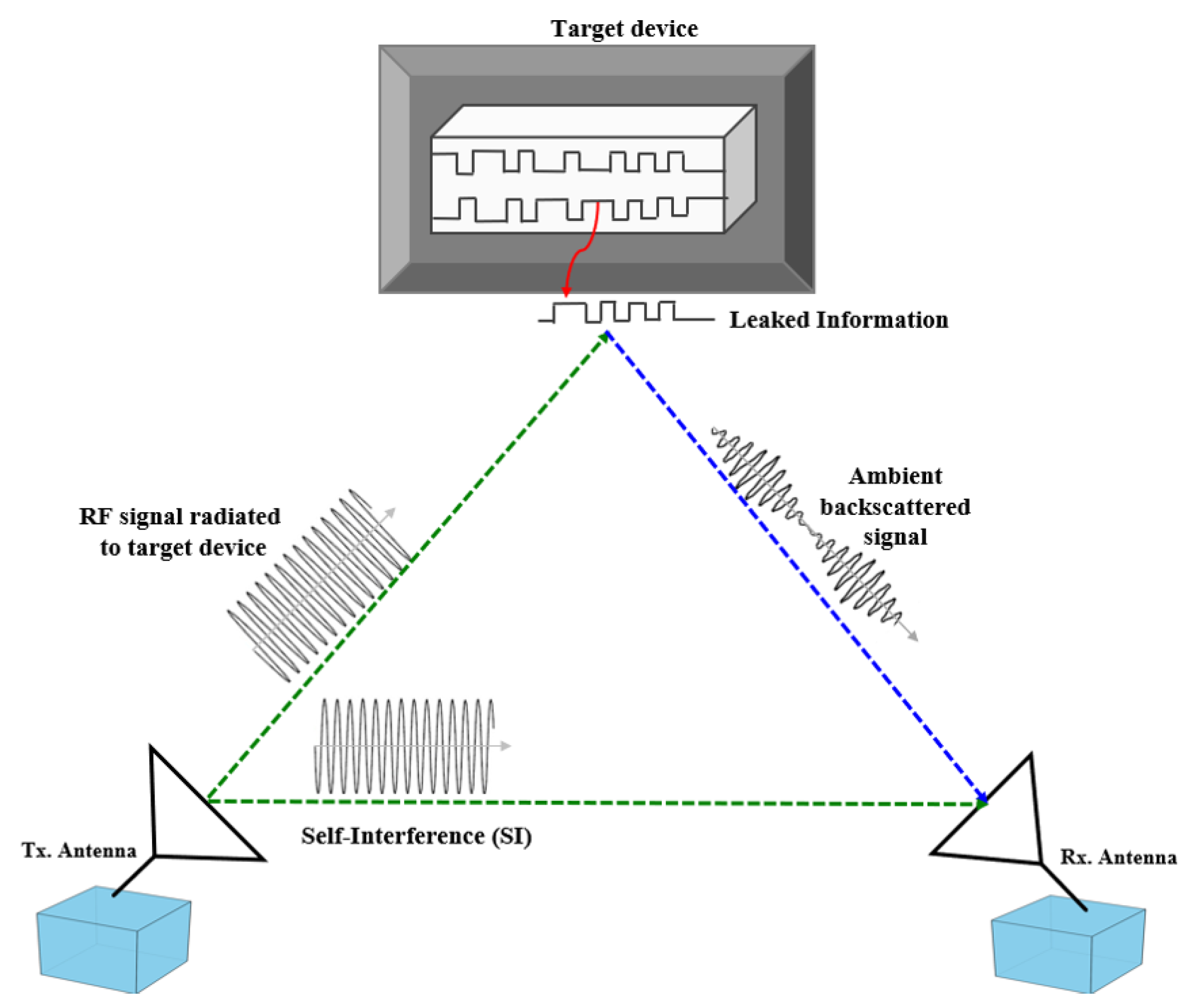
A fundamental challenge in ambient backscatter systems, especially in non-cooperative and long-range scenarios, is the presence of strong direct-path SI at the receiver, as shown in
Figure 1. The direct signal from the transmitter can be significantly stronger than the weak backscattered component, effectively obscuring the desired information-bearing signal. This issue becomes even more problematic when the backscattering mechanism does not use a dedicated antenna or controlled impedance modulation, as is the case for unintentional PCB-based backscatter. To address this issue, extensive research has investigated SI suppression and cancellation methods across various fields, such as antenna isolation, RF and analog cancellation, and digital baseband processing.
Antenna isolation is the primary defense against SI and aims to minimize coupling between the transmitter and receiver at both the physical and electromagnetic levels. In bistatic or full-duplex backscatter systems, antenna isolation is usually achieved through spatial separation, antenna orientation (polarization diversity), directional antennas, absorptive shielding, or decoupling structures [
21,
22,
23]. By physically reducing the power of the direct-path signal reaching the receiver, antenna isolation prevents front-end saturation and enhances the receiver’s dynamic range. However, analog cancellation is inherently limited by hardware imperfections such as component mismatch, limited phase shifter resolution, bandwidth constraints, and nonlinear distortions, which prevent perfect cancellation. Digital baseband processing provides the most flexible and detailed approach to SI cancellation. After down-conversion to baseband, digital algorithms can model and decrease residual SI using adaptive filters like LMS, NLMS, or Volterra-based models, as well as frequency-domain cancellation and statistical signal processing techniques [
24,
25,
26]. Digital baseband processing plays an essential and complementary role, providing detailed adaptability and modeling abilities that cannot be achieved in the physical or analog domain. Digital signal processing (DSP) techniques enable precise estimation and removal of residual SI through adaptive filtering, frequency-domain cancellation, and nonlinear modeling while also addressing impairments such as carrier frequency offset and phase noise.
However, existing studies mainly focus on intentionally designed tag antennas or cooperative backscatter nodes, where synchronization, reference signals, or structural knowledge can be utilized. In contrast, the scenario of unintentional PCB radiators under ambient bistatic illumination remains largely unexplored. These non-cooperative targets lack a predefined modulation structure, controlled synchronization, and predictable radiation characteristics, making conventional SI mitigation and carrier frequency offset (CFO) compensation techniques ineffective. Therefore, a specific post-processing framework is needed, one that directly addresses dominant SI, hardware-induced frequency offsets, and the unstructured scattering behavior of unintended PCB radiators in ambient bistatic environments.
To address these challenges, this article makes the following contributions:
Ambient Backscatter Signal Analysis under Dominant SI: We examine a practical backscatter reception scenario where the received signal is overwhelmed by a strong direct-path SI component, while the desired backscattered signal remains extremely weak. The analysis emphasizes the crucial influence of SI and CFO on baseband signal recovery in homodyne reception.
Software-Based CFO Estimation and Correction Framework: A fully digital post-processing approach is employed to estimate and correct CFO directly from measured I/Q data, avoiding the need for synchronized reference clocks, hardware-level frequency alignment, or prior knowledge of the backscattered signal parameters.
Experimental Validation under Realistic Measurement Conditions: The proposed processing chain is validated using measured ambient backscatter data collected with a homodyne receiver, demonstrating that meaningful baseband information can be recovered even in the presence of severe SI and hardware-induced frequency offsets.
The remainder of this paper is organized as follows.
Section 2 reviews related work on ambient backscatter and unintentional PCB leakage, including previous studies on intentional backscatter tags, Wi-Fi extensions, IoT applications, and SI, CFO, and phase noise in receivers.
Section 3 introduces a hierarchical, subsystem-based modeling framework that combines SIwave, HFSS, and circuit-level simulations to model PCB leakage and ambient backscatter behavior.
Section 4 describes a software-only CFO correction and backscatter recovery method for homodyne receivers operating under dominant SI, using digital processing to extract weak signals without hardware synchronization or prior knowledge of the modulation.
Section 5 explains the measurement setup and experimental validation, and the paper concludes with key findings.
2. Related Work
Ambient backscatter communication has become a promising approach for enabling ultra-low-power sensing and data transfer by utilizing existing RF signals in the environment. Initial research showed that ambient backscatter is feasible through the use of intentional tags that encode information by altering their antenna impedance states, thus reflecting incident RF signals without the need for active RF transmission or batteries [
5]. Subsequent studies expanded this concept to Wi-Fi backscatter and other ambient RF sources, emphasizing cooperative tag designs and regulated modulation schemes [
6]. Comprehensive surveys have further summarized developments in ambient backscatter systems, emphasizing applications in IoT, RFID, and passive sensing, while mainly assuming intentionally designed tag antennas and known modulation parameters [
8]. In these works, SI is often reduced through antenna isolation, geometric separation, or simplified signal models, and hardware impairments such as CFO are usually ignored or idealized.
From an electromagnetic compatibility and side-channel perspective, several studies demonstrate that PCB traces and interconnects can serve as unintended antennas, radiating or scattering signals that carry information due to switching activity in digital circuits. These unintentional emissions are widely examined in terms of electromagnetic interference (EMI) and data leakage, showing that sensitive information can be coupled into free space without a dedicated RF front end. Such findings indicate that backscattered signals can be produced and detected even when a device does not have a specific antenna. Recently, research has started to investigate how these phenomena affect wireless sensing and security-focused communication systems. While existing work confirms the presence of backscatter and leakage from unintended structures, most studies assume relatively harmless interference conditions or are focused on controlled laboratory environments. In practical ambient backscatter systems, however, the received signal is often overwhelmed by strong direct-path interference from the transmitter, which can obscure the weak backscattered signal and make signal recovery much more challenging.
Meanwhile, extensive research on full-duplex and direct-conversion receivers has explored how SI, CFO, and phase noise affect weak signal detection [
11,
12]. These studies show that even minor frequency mismatches between transmitter and receiver oscillators can lead to significant SI spreading in the baseband spectrum, greatly reducing receiver sensitivity. While ambient backscatter has been widely studied in RFID, IoT, and passive sensing, most existing research assumes intentional tag antennas, cooperative modulation techniques, or controlled impedance switching. In contrast, this work explores a significantly different and mostly uninvestigated scenario: ambient backscatter leakage from non-cooperative off-the-shelf PCBs that lack intentionally designed antennas. The backscattered signals in such systems are very weak, unstructured, and heavily masked by strong direct-path SI. Additionally, practical measurement hardware introduces unavoidable CFO and phase noise, which further disperses the SI in baseband and makes the leakage signal more difficult to detect examines a fundamentally different and mostly unexplored scenario.
To address these challenges, this paper presents a software-based post-processing framework that leverages the complex baseband representation provided by a homodyne receiver to simultaneously manage the carrier, SI, and backscattered components. Unlike previous methods that depend on antenna-level isolation, RF cancellation, or prior knowledge of modulation parameters, the proposed approach functions entirely in post-processing and does not require understanding the target signal structure or bit rate. Experimental results from a realistic bistatic measurement setup demonstrate that the CFO correction and baseband recovery pipeline markedly improve the detectability of weak ambient backscattered signals from unintentional PCB radiators.
To clearly position the contribution of this work.
Table 1 summarizes a comparison with representative recent ambient backscatter systems, highlighting differences in synchronization strategy, interference mitigation, hardware configuration, and experimental validation methodology. Unlike prior studies, the proposed approach enables ambient backscatter signal recovery without a shared reference clock and compensates residual CFO entirely in post-processing, while maintaining a practical bistatic experimental setup. Motivated by the identified limitations, the proposed framework introduces a fully asynchronous bistatic recovery approach with post-processing-based CFO compensation, as detailed in the following section.
3. System Modeling and Analysis
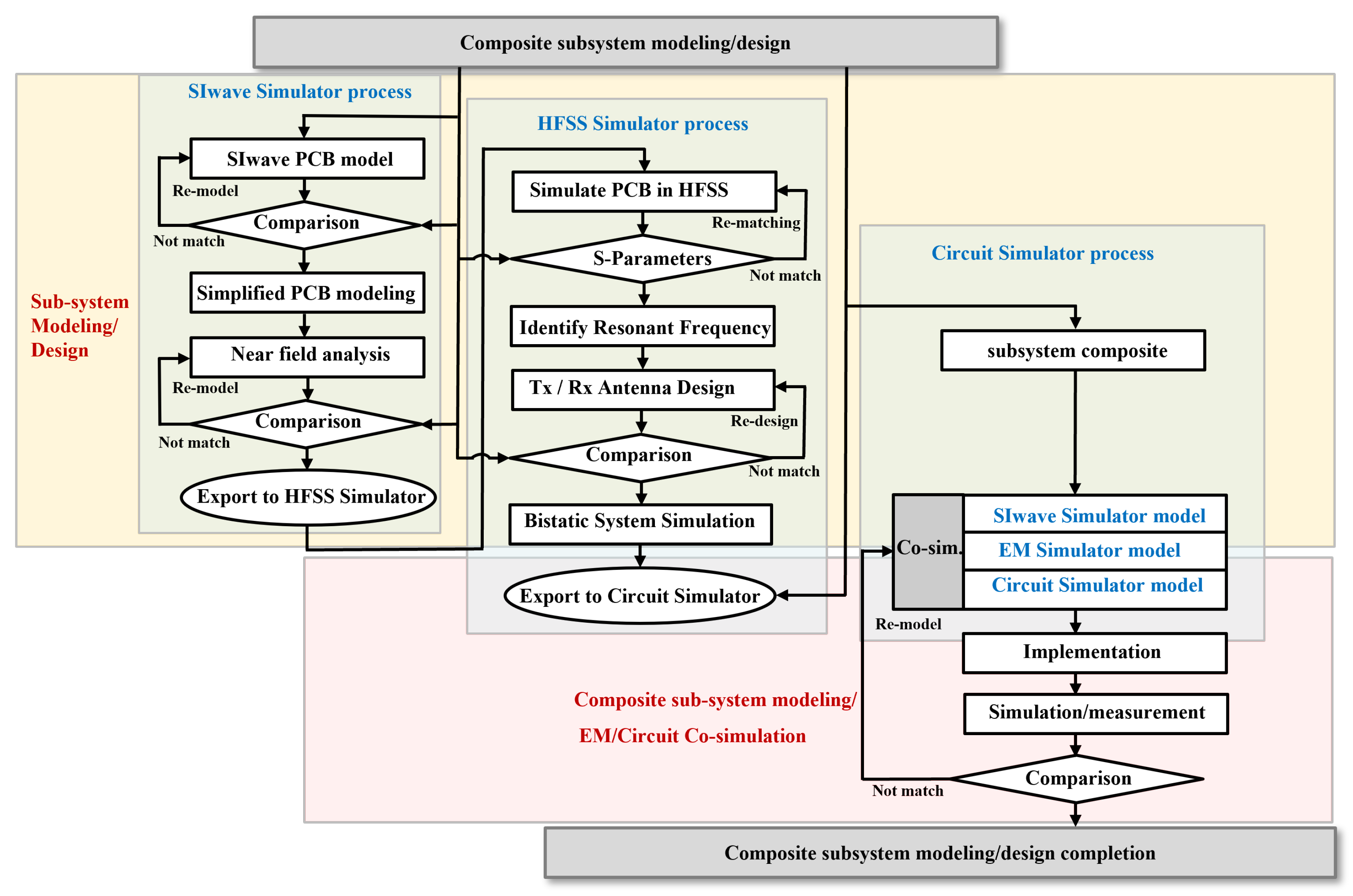
To assess the ambient backscatter leakage from off-the-shelf PCBs and capture the complex interactions between electromagnetic radiation, circuit-level behavior, and bistatic backscatter mechanisms, a hierarchical subsystem-based modeling approach is used. Because of the limitations of any single simulation tool in simultaneously handling full-wave electromagnetic propagation and time-varying circuit behavior, the overall system is broken down into multiple subsystems, each modeled and analyzed with the most suitable dedicated simulation environment, as shown in
Figure 2.
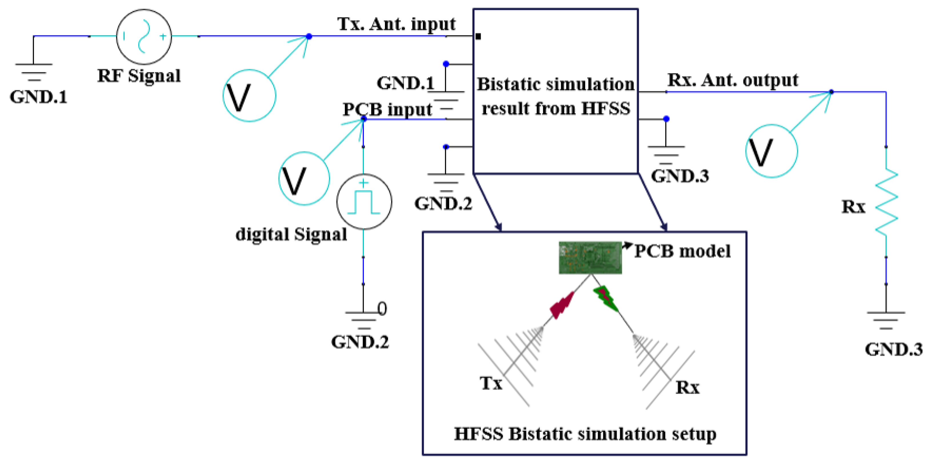
After characterizing each individual subsystem, a dynamic EM/Circuit co-simulation framework is employed to integrate the electromagnetic and circuit domains into a unified system-level model within the Ansys Electronics Desktop (AEDT) circuit simulator, as shown in
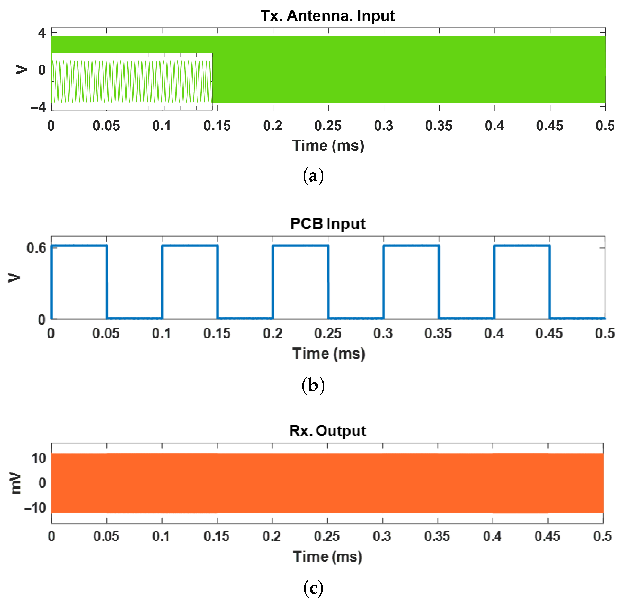
Figure 3. The workflow begins with exporting the PCB model from SIwave to HFSS. In HFSS, a bistatic simulation is configured using two identical dedicated antennas, positioned as transmit (Tx) and receive (Rx), and oriented toward the PCB. The Tx antenna illuminates the PCB, enabling frequency-domain characterization of the backscattered and reradiated responses under the bistatic setup. The frequency-domain response is exported as a three-terminal S-parameter (S3P) model, where terminal 1 is the Tx input, terminal 2 the PCB input, and terminal 3 the Rx output. The referenced labels (GND.1, GND.2, and GND.3) indicate the corresponding signal return paths within the co-simulation structure. For transient (time-domain) analysis assigns each terminal to the appropriate source and voltage probe within the AEDT Circuit Simulator. In operation, the Tx antenna illuminates the PCB with a continuous-wave RF signal, as shown in
Figure 4a, where the dense sinusoidal pattern depicts the continuous RF carrier, with an overlaid sinusoid for visual clarity.
In this simulation, the Tx input is set as a 1.5505 GHz carrier with an amplitude of 3.9 V, aligning with practical measurement setups. This CW excitation couples into the PCB structure, inducing a weak reradiated (backscattered) component that carries the corresponding baseband signal propagating along the PCB trace. For demonstration, a 0.6 V amplitude baseband signal at 10 kHz is applied along the PCB trace, as shown in
Figure 4b. These values are chosen to ensure clear time-domain visualization of the induced baseband variation while remaining within practical operating conditions, without altering the general leakage mechanism being modeled. This methodology enables realistic evaluation of ambient bistatic backscatter generation and reradiation under typical operating conditions, effectively bridging the gap between isolated subsystem simulations. By leveraging the strengths of SIwave, HFSS, and circuit-level simulation, the proposed modeling framework offers a comprehensive and efficient platform for analyzing unintentional electromagnetic leakage mechanisms in complex PCB-based systems.
This co-simulation framework replicates the physical illumination and PCB backscattering mechanisms of the experimental setup. While the simulation uses virtual connections between SIwave, HFSS, and the circuit simulator, it accurately models the fundamental physical interactions, including electromagnetic propagation from the Tx antenna, reflection and reradiation by the PCB, and reception at the Rx antenna. The only difference is that, in the simulation, signals pass through modeled components instead of real hardware, whereas in the experiment these interactions occur in the physical domain with actual devices, as explained later in
Section 5. A key challenge in this ambient bistatic backscatter EM/Circuit co-simulation scenario is that the receiver simultaneously captures a strong direct-path component from the transmitter, commonly referred to as SI. Because this direct-path SI can be orders of magnitude stronger than the weak backscattered signal from the PCB, it can dominate the received waveform and mask the modulation of interest, as shown in
Figure 4c. This large power disparity significantly reduces the effective SNR and makes it difficult to isolate and recover the backscattered information, particularly when the backscattered amplitude is further attenuated by propagation loss and imperfect coupling. Therefore, effective suppression of the dominant SI together with appropriate post-processing to enhance the weak backscattered component is essential for reliable baseband recovery at the receiver.
3.1. Direct Conversion (Zero-IF) Receiver
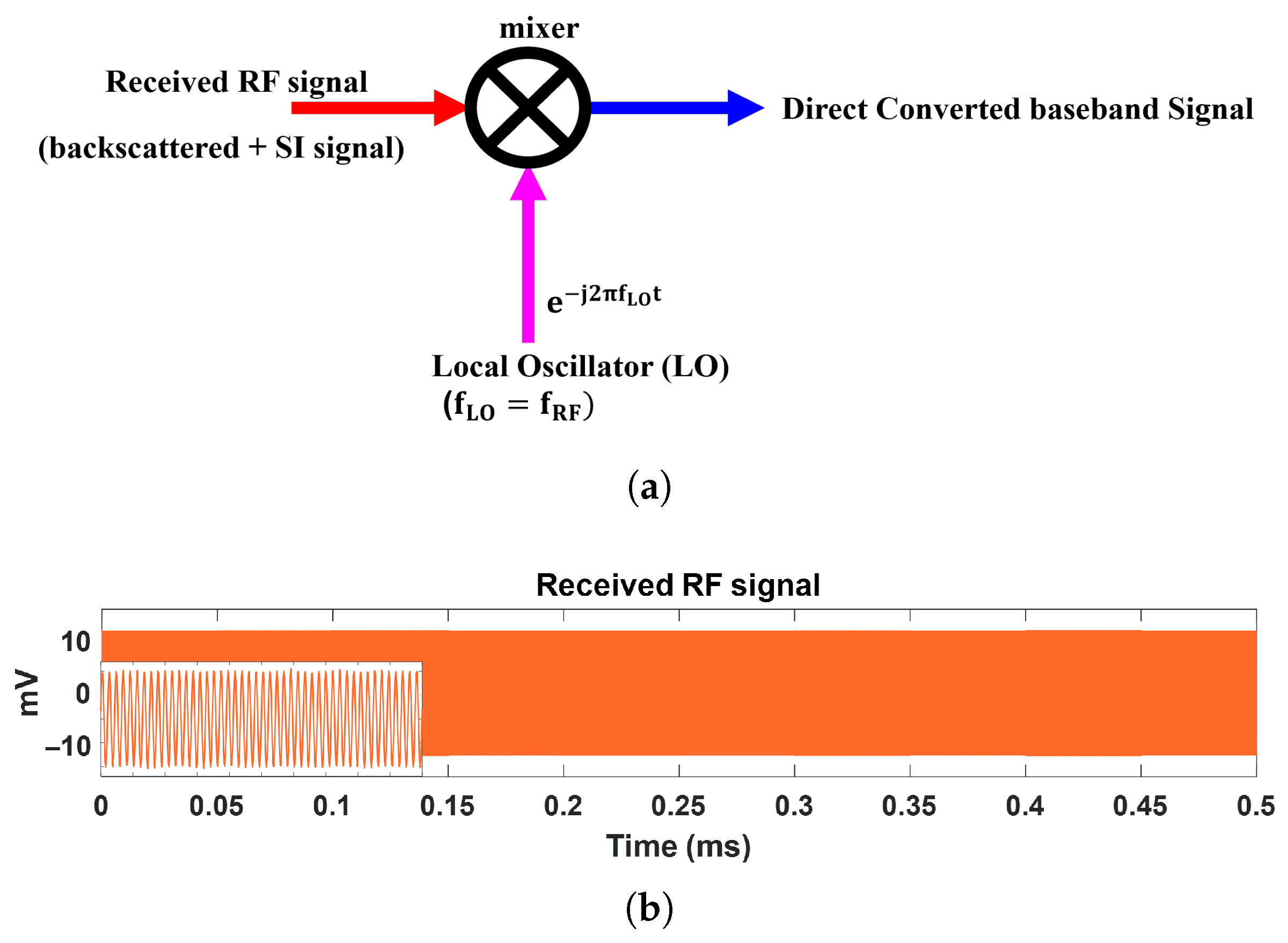
An important observation in bistatic backscatter systems is that both the SI and the desired backscattered signal occupy the same carrier frequency. This frequency coherence can be advantageously exploited at the receiver by employing a direct-conversion (homodyne receiver) in which the received RF signal is mixed directly to baseband using a local oscillator (LO) tuned to the carrier frequency. As illustrated in
Figure 5a the receiver LO is intentionally aligned with the transmitted carrier to enable coherent downconversion.
Figure 5b shows a retaken view of
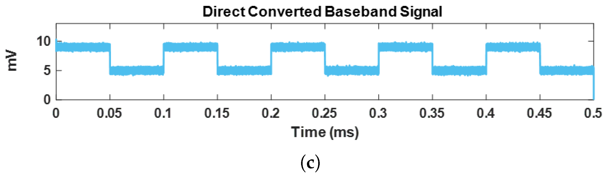
Figure 4c, presenting the simulated received RF waveform in which the weak backscattered PCB component is heavily dominated by SI. At the RF stage, the desired signal is not visually distinguishable due to the large amplitude disparity. By applying the direct-conversion process, the received RF signal is mixed with the synchronized LO. Because the SI shares the same carrier frequency, it is effectively derotated to DC after mixing. As a result, the dominant SI component is translated to a near-constant (DC) term in the baseband domain. This property allows the SI to be efficiently mitigated using standard DC-offset removal techniques without requiring complex adaptive cancellation. The resulting downconverted signal is shown in
Figure 5c, where the desired backscattered variation becomes observable in the baseband waveform. This demonstrates that coherent direct conversion transforms the SI problem from a high-power RF interference issue into a manageable DC-offset suppression task in baseband processing. While coherent direct conversion facilitates observation of the backscattered signal in baseband, several practical challenges remain in implementing such receivers, especially in the case of dominant SI scenarios. The following subsection discusses these challenges in detail, focusing on the practical limitations of direct-conversion architectures in ambient backscatter systems.
Challenges
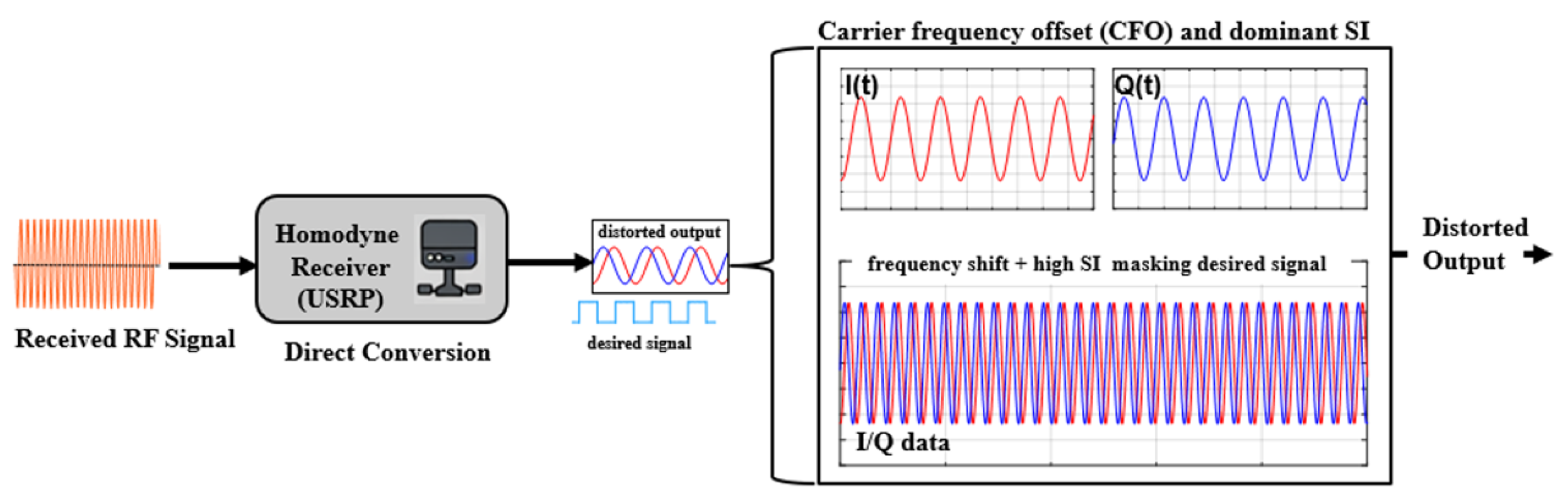
While homodyne receivers offer significant advantages for bistatic backscatter systems, their performance is inherently sensitive to CFO between the transmitter and the receiver. CFO arises from inevitable mismatches between the local oscillators of the RF source and the receiver, as well as from phase-locked loop (PLL) imperfections and frequency drift. In direct-conversion architectures, this offset manifests directly at baseband as a time-varying phase rotation, affecting both SI and the desired backscattered signal. In the presence of dominant SI, even a small CFO can have a pronounced impact on the received baseband signal. Specifically, CFO causes the strong SI component to spread in the baseband spectrum, generating low-frequency oscillations and spectral leakage that can overlap with the frequency band of the weak backscattered signal. As a result, the modulation carried by the backscattered component is masked or distorted, significantly degrading the SNR and complicating subsequent detection and thresholding processes, as shown in
Figure 6.
The mathematical description of CFO effects in a homodyne backscatter receiver. Let the transmitted CW excitation be given by (1)
where
,
are amplitude and carrier frequency respectively. In a bistatic backscatter setup, the receiver detects a combination of a strong direct-path SI and a weak backscattered component, which can be represented as (2)
where
and
denote the complex channel coefficients of the SI and backscatter paths, respectively,
and
are the corresponding propagation delays,
is the baseband modulation signal, and
represents complex Gaussian noise. For analytical tractability, the backscattering channel is modeled using a single complex coefficient
, representing the effective amplitude attenuation at the selected operating frequency.This single coefficient provides a reasonable first-order approximation, while the experimental measurements inherently account for any residual propagation effects present in the environment. In this work, the noise term is modeled as complex Gaussian noise, which is a standard assumption for initial system-level analysis. Alternative non-Gaussian distributions were not explicitly considered because the received signal is dominated by SI and residual CFO. Under these conditions, system performance is primarily limited by SI and CFO rather than the specific statistical properties of the noise. Nevertheless, in environments with strong impulsive interference or non-Gaussian disturbances, alternative noise models could be incorporated to further refine the analysis. In a direct-conversion receiver, r(t) is mixed by an LO as shown in (3)
where
is the receiver local oscillator (LO) frequency. After low-pass filtering, the complex baseband signal can be expressed as (4)
where
denotes the CFO, and
represents the down-converted noise. This expression highlights that CFO introduces a common time-varying phase rotation
that multiplies both the SI and backscattered components. When
, the received baseband is dominated by the SI term, and the CFO-induced rotation makes the SI appear nonstationary at baseband. In practice, this results in spectral leakage and low-frequency oscillations that can overlap with the modulation bandwidth of
, thereby masking the weak backscattered information. In magnitude-based demodulation (envelope detection), the observed signal envelope is given by (5).
showing that the weak backscattered modulation is embedded as a small perturbation on top of the dominant SI amplitude by ignoring noise and small delay differences.From this analysis any residual CFO/phase-noise-induced fluctuations of the strong SI term can directly degrade the detectability of the backscattered signal, motivating explicit CFO estimation/compensation prior to SI suppression and baseband recovery. Therefore, accurate estimation and compensation of CFO are essential for effective SI suppression.
4. CFO Correction and Backscattered Signal Recovery Under Dominant SI via Post-Processing
As discussed in the previous subsection, CFO plays a critical role in degrading the performance of homodyne backscatter receivers under dominant SI. In practical bistatic measurement environments, pre-correction or hardware-level synchronization of frequency offsets is often infeasible due to inherent non-idealities of the measurement setup. Specifically, CFO may arise from multiple sources, including (i) independent and unsynchronized local oscillators at the transmitter and receiver with parts-per-million (ppm) frequency mismatch, (ii) the absence of a shared reference clock such as a common 10 MHz reference or GPS-disciplined oscillator (GPSDO), (iii) Doppler shifts caused by relative motion between system components, (iv) sampling clock offsets in the ADC/DAC stages, and (v) small frequency mis-tuning or drift in down-conversion hardware. Even when these offsets are small in absolute terms, their impact is amplified in bistatic backscatter systems due to the extreme power imbalance between the dominant SI and the weak backscattered signal.
Since these impairments stem from hardware imperfections and environmental factors, they cannot be fully eliminated through analog or RF design alone. Therefore, digital post-processing CFO correction becomes crucial. In our proposed algorithm, CFO is directly estimated from the measured complex baseband signal acquired from the homodyne receiver. Due to the dominance of the SI component, the frequency offset appears as a strong spectral peak near DC in the baseband spectrum. By applying a fast Fourier transform (FFT) to the received I/Q data, the residual frequency shift can be precisely identified without prior knowledge of the backscattered signal’s characteristics. Once the CFO is estimated, digital frequency correction is applied by mixing the received baseband signal with a locally generated complex exponential at the estimated offset frequency. This process effectively removes the time-varying phase rotation caused by CFO and restores stationarity to the SI component in the baseband domain. After CFO correction, low-pass filtering suppresses out-of-band noise and residual high-frequency artifacts, allowing clearer observation of the envelope modulation caused by the backscattered signal. To further improve the detection of the weak backscattered component, envelope detection is performed on the CFO-corrected signal, followed by DC offset removal to eliminate the dominant constant component associated with residual SI. Finally, an adaptive thresholding scheme distinguishes between high and low modulation states in the recovered baseband waveform. This fully digital processing chain enables reliable extraction of the weak backscattered information despite severe SI and hardware-induced frequency offsets. Algorithm 1 summarizes the software-based CFO correction and baseband recovery process implemented entirely in post-processing, without the need for hardware synchronization between the transmitter and receiver.
This approach lies in its software-only correction framework, which does not rely on synchronized clocks, specialized RF cancellation hardware, or prior knowledge of the backscattered modulation parameters. Unlike conventional CFO correction scenarios, where the desired signal is directly observable or supported by pilot symbols [
30], the present work operates under extreme SI dominance, with the weak ambient backscatter deeply buried beneath the CFO-broadened SI. Consequently, even small residual CFO errors prevent sufficient spectral re-concentration of the SI component and hinder successful envelope recovery. The effectiveness of Algorithm 1 therefore lies in exploiting the dominant SI component itself for accurate digital frequency alignment, enabling recovery of the buried leakage signal through purely digital post-processing without any hardware modification. By leveraging the inherent properties of the dominant SI in a homodyne bistatic receiver, the proposed method enables practical recovery of weak ambient backscattered signals under realistic measurement conditions, making it well suited for experimental and sensing-oriented backscatter systems. Based on the proposed CFO correction and baseband recovery framework, experimental measurements were conducted using a bistatic backscatter setup with a homodyne receiver. The measured I/Q data were processed entirely in software, following the steps outlined in Algorithm 1. The experimental results presented in the next section demonstrate the effectiveness of the proposed approach in suppressing dominant SI, compensating hardware-induced frequency offsets, and recovering weak backscattered baseband signals under realistic measurement conditions.
| Algorithm 1: Software-Based CFO Correction and Ambient Backscattered Signal Recovery under Dominant SI |
Input: Measured complex baseband signal , sampling frequency , CFO search bandwidth B, DC guard , LPF cutoff frequency Output: Recovered digital baseband signal 1 Initialization: 2 , ; 3 Step 1: DC Offset Removal 4 ; 5 Step 2: FFT-Based CFO Estimation 6 ; // Windowing 7 ; // Spectrum 8 ; // Freq. axis 9 ; // Search region 10 ; 11 ; 12 Step 3: Digital CFO Compensation 13 ; 14 Step 4: Complex Baseband Low-Pass Filtering 15 ; 16 Step 5: Envelope Extraction 17 ; 18 Step 6: Envelope DC Removal and Smoothing 19 ; 20 ; 21 Step 7: Adaptive Thresholding and Bit Recovery 22 Compute adaptive threshold from ; 23 ; 24 return ; |
5. Measurement Setup and Experimental Validation
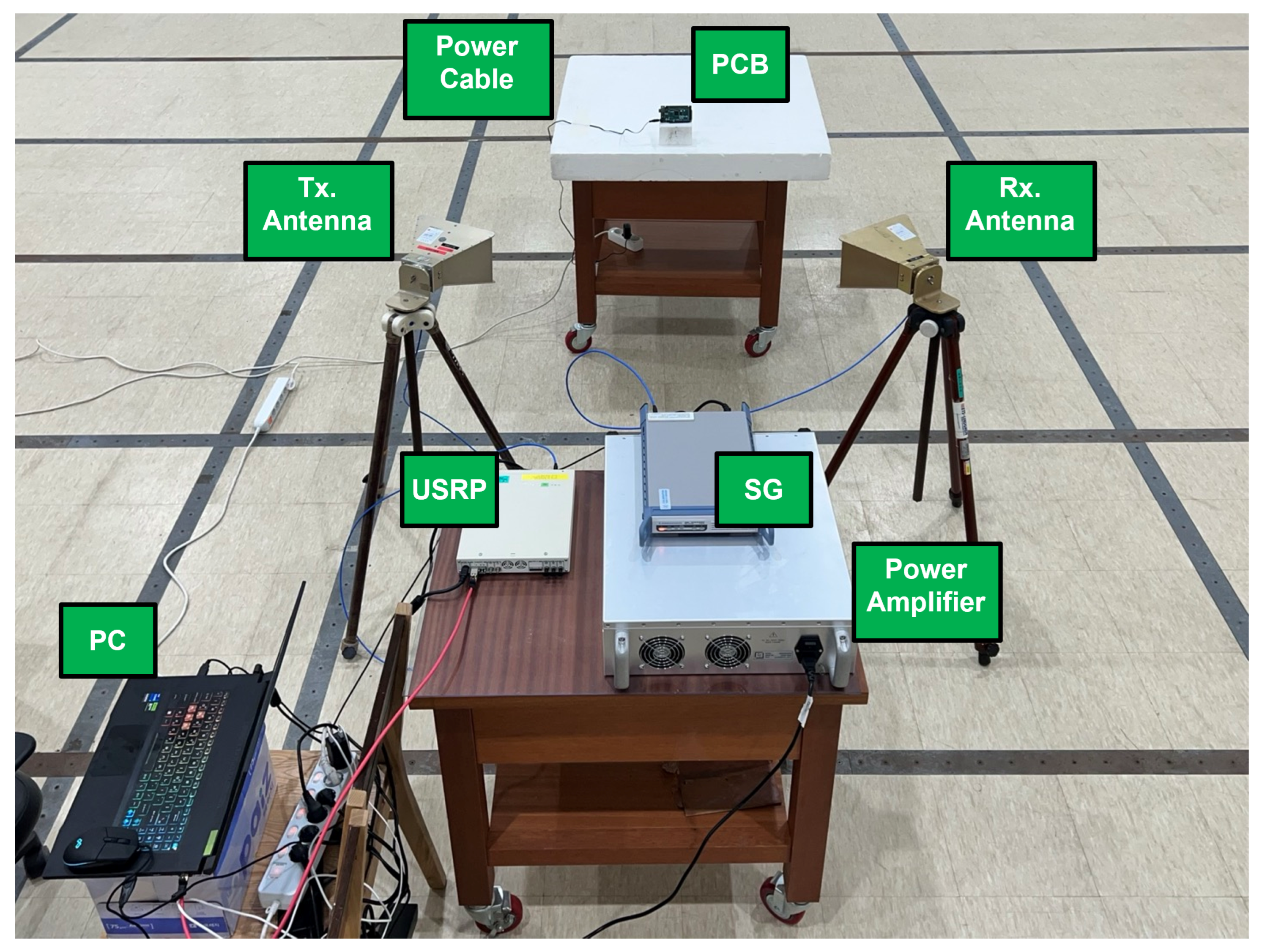
To validate the proposed software-based CFO correction and baseband recovery framework under realistic conditions, a bistatic backscatter measurement setup was implemented, as illustrated in
Figure 7. The experimental configuration closely follows the simulation framework described in the previous section while incorporating practical hardware non-idealities commonly encountered in real ambient backscatter systems.
The measurement system includes two identical horn antennas, one acting as the transmitter (Tx) and the other as the receiver (Rx), along with a Universal Software Radio Peripheral (USRP) configured as a homodyne (direct-conversion) receiver. The Tx and Rx antennas are separated and positioned to face an off-the-shelf printed circuit board (PCB), which functions as the target device for ambient backscattering. In this setup, the distance between the Tx antenna and the PCB, as well as between the PCB and the Rx antenna, is adjustable from 30 cm to 1 m. The Tx antenna continuously transmits a single-tone RF carrier at a maximum power of 20 dBm, illuminating the PCB. The incident RF signal couples into the PCB and interacts with its internal circuitry, generating a weakly modulated backscattered signal that is reradiated into free space. This scattered signal, which contains leaked baseband information, is then captured remotely by the Rx antenna.
The experiments were conducted at a carrier frequency of 1.5505 GHz using a signal generator (SG) to generate the transmitted signal, and a USRP X300 was used as the receiver operating at a sampling rate of 1 MS/s. Standard horn antennas (HRN-0118) were arranged in a bistatic configuration. No shared external reference clock was employed between the SG and the USRP receiver; residual CFO was compensated digitally using Algorithm 1. The experimental equipment is listed in
Table 2, and the corresponding measurement parameters are summarized in
Table 3.
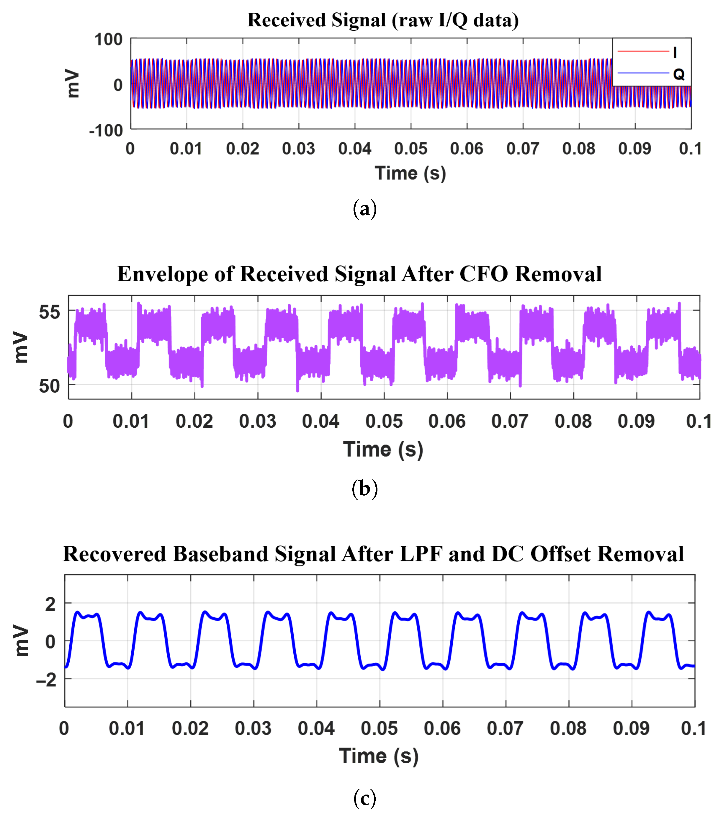
Figure 8a presents the signal measured at the receiver, where the weak backscattered component is completely obscured by the strong direct-path SI and further distorted by the residual carrier frequency offset (CFO). As a result, no discernible baseband information can be identified in the raw waveform. To reveal the weak backscattered component masked by SI, software-based CFO compensation is applied to the measured I/Q data. After CFO correction, the extracted envelope exhibits clear amplitude transitions, indicating the presence of the underlying backscattered baseband information, which is not observable in the raw waveform, as shown in
Figure 8b. Finally, the CFO-corrected envelope is filtered by low-pass filtering, and DC-offset removal is applied to suppress residual harmonics and baseline bias, producing a cleaner recovered baseband waveform, as shown in
Figure 8c. The resulting waveform exhibits distinct high and low states, demonstrating that weak backscattered information can be successfully extracted from an off-the-shelf PCB despite severe SI and hardware-induced impairments. These results correspond to the measurement setup in which the target PCB is located 30 cm from both the transmitter and the receiver.
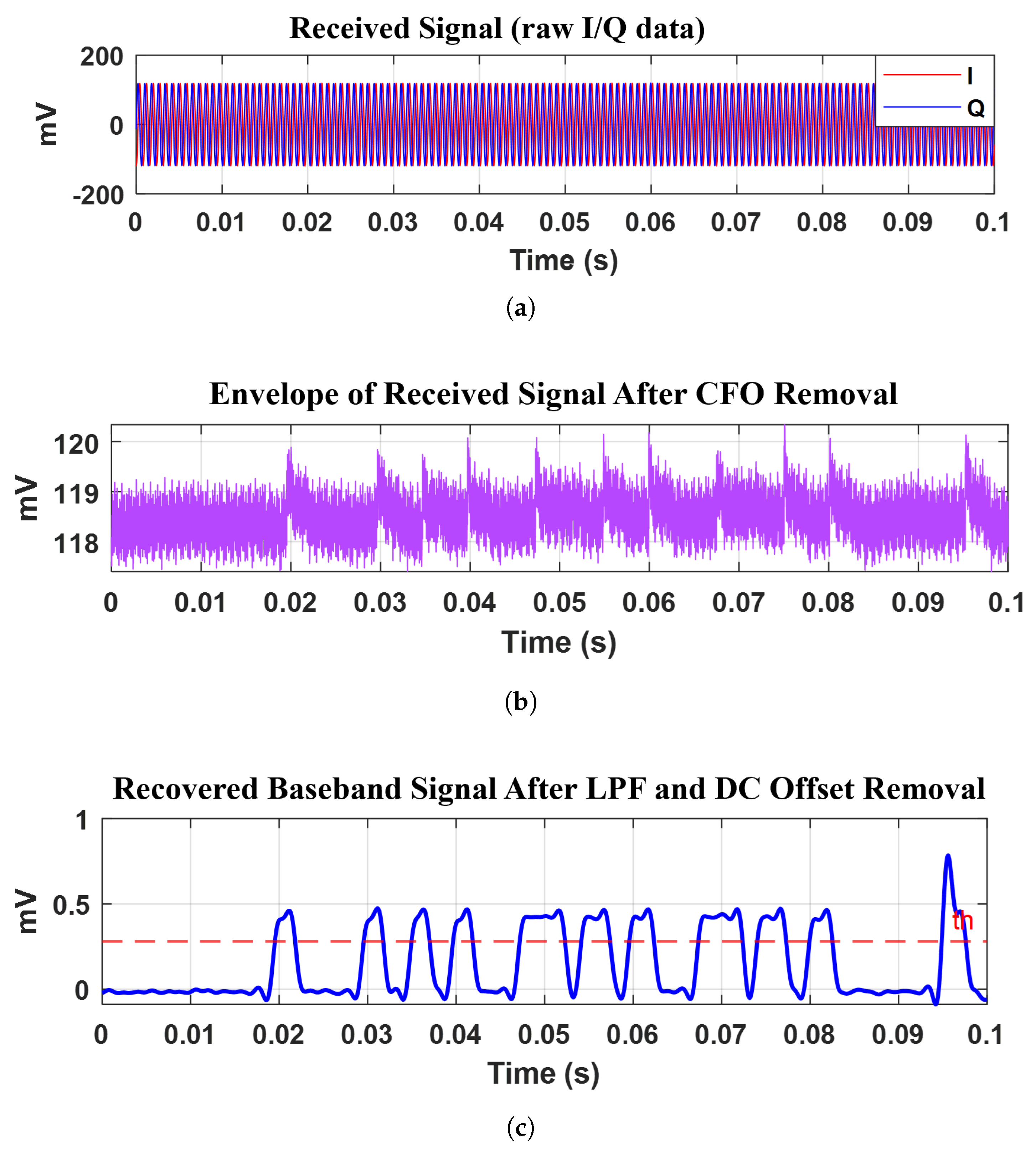
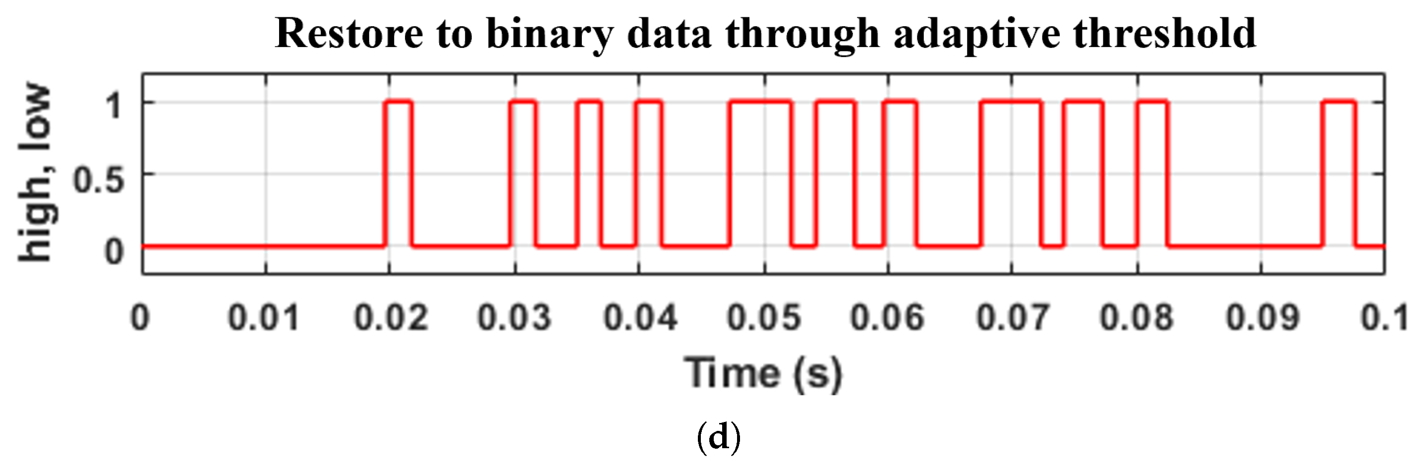
To further demonstrate the proposed leakage-recovery framework, additional measurements were conducted with both the Tx–PCB and PCB–Rx separation distances set to 1 m. In this case, instead of using an ideal digital pattern with equal high- and low-state durations, a real ASCII plain-text sequence was transmitted. At this distance, the backscattered component experiences significant path loss and decreased coupling, resulting in an extremely weak leakage signal at the receiver. Nevertheless, by applying the proposed post-processing algorithm, the recovered waveform shows clear transitions corresponding to the intended signal. The related results are shown in
Figure 9b–d. These results confirm that leakage information can still be extracted even when the scattered signal is severely attenuated, highlighting the practical applicability of the proposed method in realistic ambient bistatic backscatter scenarios. Overall, the 1 m measurement demonstrates that reliable baseband recovery is achievable beyond short-range coupling conditions, as long as dominant SI and frequency-offset effects are properly mitigated in the digital domain. The results confirm that, despite dominant SI and residual CFO, the proposed post-processing framework can recover the ambient backscattered signal from an unintentional radiator PCB under controlled conditions, demonstrating the feasibility of the approach approach.
5.1. Performance Evaluation
The proposed SI-dominated backscatter system relies on accurate CFO compensation for reliable demodulation. Residual frequency offset leads to continuous phase rotation, spectral leakage, and distortion of the weak backscattered signal. Therefore, CFO estimation accuracy is the main factor affecting overall system performance. To evaluate the CFO estimator under realistic conditions, a measured composite waveform captured with a USRP receiver was used. Since the received signal includes a dominant SI and a weak backscattered signal sharing the same carrier frequency offset, the CFO is mainly determined by the strong SI tone. For performance assessment, the measured waveform is treated as the clean reference signal. Controlled additive white Gaussian noise (AWGN) is synthetically added to create a desired signal-to-noise ratio (SNR). The SNR is defined as (6)
where
denotes the total received signal power, and
is the variance of the injected noise. Since the SI power significantly exceeds the backscattered signal power, the total signal power is effectively dominated by the SI component.
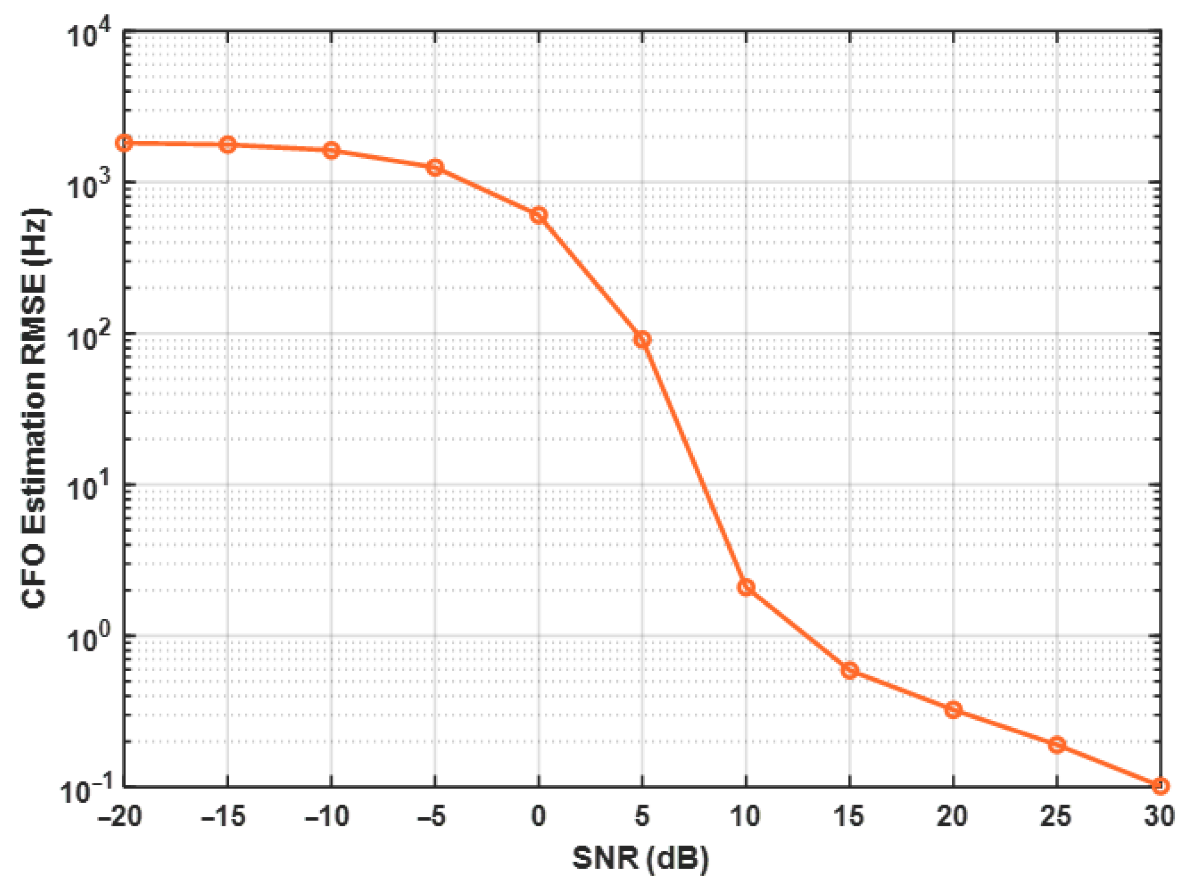
For each SNR value, multiple Monte Carlo trials are conducted. In each trial, independent AWGN is added to the measured waveform, the CFO is re-estimated, and the root-mean-squared error (RMSE) is calculated based on the CFO estimated from the original measurement. This process isolates the noise sensitivity of the CFO estimator while maintaining the realistic SI-dominated signal structure of the hardware measurement.
Figure 10 illustrates the RMSE of the CFO estimator as a function of the SNR. The figure shows that the estimator’s accuracy improves as the SNR increases, indicating the reduced noise influence on the CFO estimation. This confirms the robustness of the proposed method under realistic SI-dominated measurement conditions. To evaluate practical feasibility further, the computational complexity of the post-processing algorithm is examined. The dominant operation is frequency estimation, which has a theoretical complexity of
for the FFT-based implementation, while memory usage scales linearly as
.
5.2. Limitation
While the FFT-peak CFO estimator effectively recovers weak PCB-originated backscatter in scenarios dominated by a single SI tone, its performance may decline under more challenging conditions. Excessive transmitter or receiver phase noise can broaden the SI spectrum and reduce peak sharpness. Multipath propagation may create multiple comparable SI tones, and receiver impairments such as IQ imbalance or DC offset can distort the baseband spectrum. When no single dominant SI tone exists or the leakage signal approaches the noise floor, the estimator may fail, highlighting the operational limits of the current method. Future work will explore advanced multi-tone or iterative frequency refinement techniques to develop a more robust framework for SI-dominated backscatter.