

Article

A 12-Bit, 10 MS/s Two-Step Sub-Ranging SAR ADC with Top-Plate Dividing

1
Samsung Electronics, Hwasung 18450, Republic of Korea
2
Division of Semiconductor and Electronic Engineering, Hankuk University of Foreign Studies, Yongin 17035, Republic of Korea
*
Author to whom correspondence should be addressed.
Electronics 2026, 15(5), 1050; https://doi.org/10.3390/electronics15051050
Submission received: 29 January 2026 / Revised: 27 February 2026 / Accepted: 28 February 2026 / Published: 3 March 2026
(This article belongs to the Section Circuit and Signal Processing)

Abstract

In this paper, a 12-bit, 10 MS/s two-step sub-ranging successive approximation register (SAR) analog-to-digital converter (ADC) is proposed. The proposed architecture enables residue amplification within a single-stage SAR ADC by dividing the top-plate sampling node, thereby avoiding the requirement for a multi-stage design. This structure also eliminates gain and offset mismatches between the coarse and fine conversions, enhancing robustness and linearity. Owing to the two-step operation, the total capacitance of the capacitive digital-to-analog converter (CDAC) is reduced by 86% compared to that of a conventional SAR ADC with the same unit-capacitor size. In addition, the residue amplifier drives only one-fourth of the total CDAC capacitance, significantly relaxing its power consumption. A prototype fabricated in a 65 nm CMOS process occupies an area of 252 μ m × 227 μ m and demonstrates a signal-to-noise and distortion ratio (SNDR) of 65.7 dB at Nyquist-rate input. The total power consumption is 227.7 μ W under a 1.2 V supply, resulting in a Walden figure of merit (FoM) of 14.5 fJ/conversion step. These results confirm competitive performance and energy efficiency, even with the use of an analog residue amplifier.

1. Introduction

SAR ADC is widely adopted for applications that require medium resolution and moderate bandwidth due to its excellent power efficiency [1,2,3]. However, maintaining such efficiency at higher resolutions remains challenging because both thermal noise and circuit non-idealities become dominant. The primary limiting factors include the input-referred noise of the dynamic comparator and the nonlinearity caused by CDAC mismatch.
In a conventional SAR architecture, the CDAC typically employs a binary-weighted capacitor array. As the resolution increases, the capacitor ratio grows exponentially, and mitigating mismatch errors requires larger unit capacitances. This inevitably results in an exponential increase in total CDAC capacitance, which not only elevates the ADC core’s switching energy but also increases the load of peripheral blocks such as the reference buffer and digital logic, thereby degrading the overall power efficiency. While digital calibration techniques [4,5] can correct capacitor mismatches, they incur additional digital hardware, longer data latency, and higher power consumption.
Another key challenge lies in reducing the comparator noise. The comparator power increases by a factor of four to achieve a 6 dB reduction in noise [6]. To mitigate this, pipelined SAR architectures [7,8,9] have been proposed, where a residue amplifier enhances the effective resolution by amplifying the remaining voltage before the fine conversion. However, pipelined SAR ADCs suffer from errors induced from the gain and offset mismatches owing to the use of multiple amplification stages. Alternatively, statistical approaches [10,11,12] have been explored to suppress the noise of the comparator by performing repeated comparisons at the same input voltage level. Despite their noise reduction capability, these approaches result in considerable power and area overhead because they require a large number of comparison cycles and post-processing circuitries.
Cyclic ADC architectures are also attractive due to their hardware reuse mechanism and compact core area. In [13], cyclic ADC using an open-loop residue amplifier was adopted for low-power operation, with the degradation of the open-loop amplifier’s linearity due to its limited input range alleviated by a capacitive source degeneration topology. However, cyclic ADCs require N time of the amplification phase for N-bit resolution, and signal range of the amplifier should be wide enough. In addition, open-loop amplification makes cyclic ADCs vulnerable to PVT variation.
To further improve energy efficiency, various CDAC switching schemes have been developed to minimize both switching energy and total capacitance. Compared with conventional switching, V C M -based [14], monotonic [15], and charge-redistribution [16] switching methods significantly reduce the CDAC switching power, contributing to the overall power savings of high-resolution SAR ADCs.
In this paper, we present a two-step sub-ranging SAR ADC. By dividing the top-plate sampling CDAC node, residue amplification is carried out within a single-stage CDAC rather than in separated gain stages. This two-step approach using V C M -based switching relaxes the noise requirements of the comparator and reduces the total CDAC capacitance by 86% compared to a conventional SAR ADC, leading to a significant power reduction. Furthermore, since the residue amplifier only drives combined coarse and fine capacitance equivalent to one-fourth of the total CDAC, it can save the bias current of the amplifier. To further enhance energy efficiency, a switching operational amplifier (op-amp) technique is employed [7], which turns off the amplifier during the conversion phase. The remainder of this paper is organized as follows. Section 2 describes the structure of the proposed ADC and its operations, and Section 3 presents circuit implementations of the residue amplifier and CDAC. The measurement results and conclusions are presented in Section 4 and Section 5.

2. Structure of the Proposed ADC

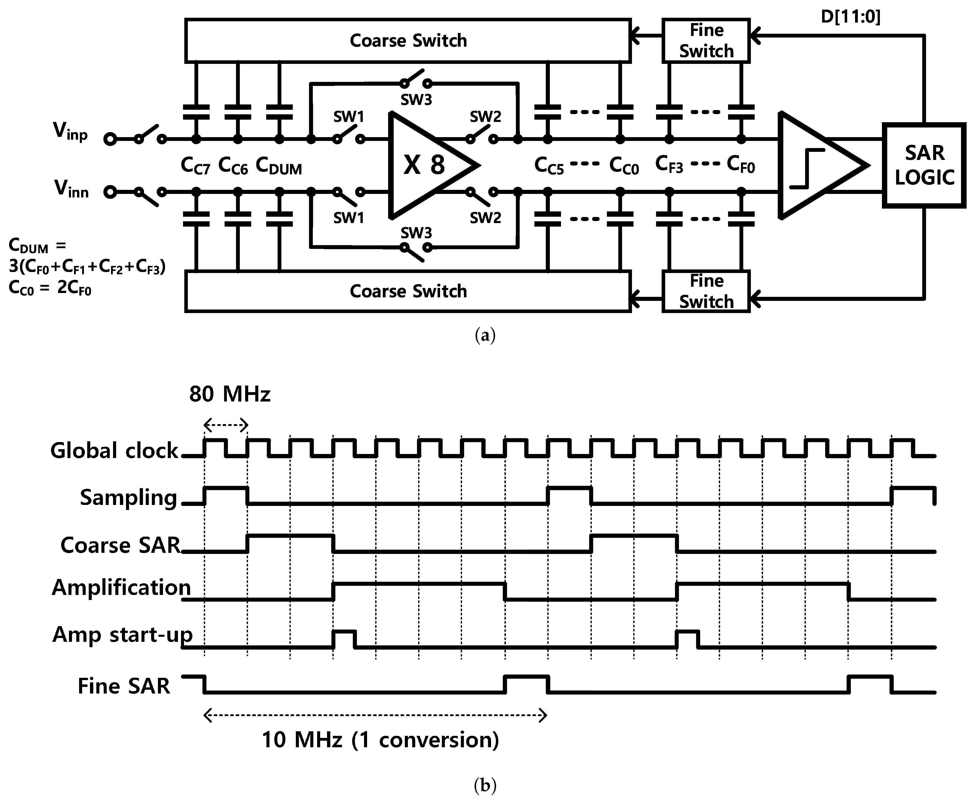
Figure 1a illustrates the top block diagram of the proposed ADC. The differential input voltage is sampled by bootstrapped switches to achieve sufficient linearity. Compared to a conventional SAR ADC, a residue amplifier and division switch (SW1, SW2, and SW3) are introduced to split the top-plate node of the CDAC. The CDAC consists of 8-bit coarse and 4-bit fine binary-weighted capacitor segments. It achieves a coarse 8-bit and fine 5-bit resolution using the V C M -based switching method [1]. The division switch, placed between the dummy capacitor ( C D u m ) and C C 5 , separates the top-plate node. The input of the amplifier is connected to the left side of the division switch, while its output drives the right side. Among the capacitor arrays comprising the CDAC, the coarse conversion operates by switching C C 7 C C 0 . The dummy capacitor ( C D u m ) is never switched. During the coarse conversion phase, C D u m and C F 3 C F 0 function as attenuation capacitors, resulting in a conversion gain given by
G c o a r s e = n = 0 7 C C n C D u m + n = 0 3 C F n + n = 0 7 C C n .
Likewise, during the fine conversion phase, C C 5 C C 0 act as attenuation capacitors, yielding the fine conversion gain as
G f i n e = A C L · n = 0 3 C F n n = 0 5 C C n + n = 0 3 C F n ,
where A C L is the closed-loop residue amplifier gain. The coarse and fine conversion gain should be matched for proper ADC scaling. Thus, the unit capacitance of the coarse CDAC (4 fF) is twice that of the fine CDAC (2 fF), and C D u m is designed to be three times larger than the sum of C F 3 to C F 0 to avoid gain mismatch between the coarse and fine CDAC arrays. The residue amplifier gain is set to a factor of eight to compensate for large attenuation during the fine conversion phase. The load at the amplifier output is only one-fourth of the total CDAC capacitance, leading to saving in terms of power consumption.

2.1. Operation

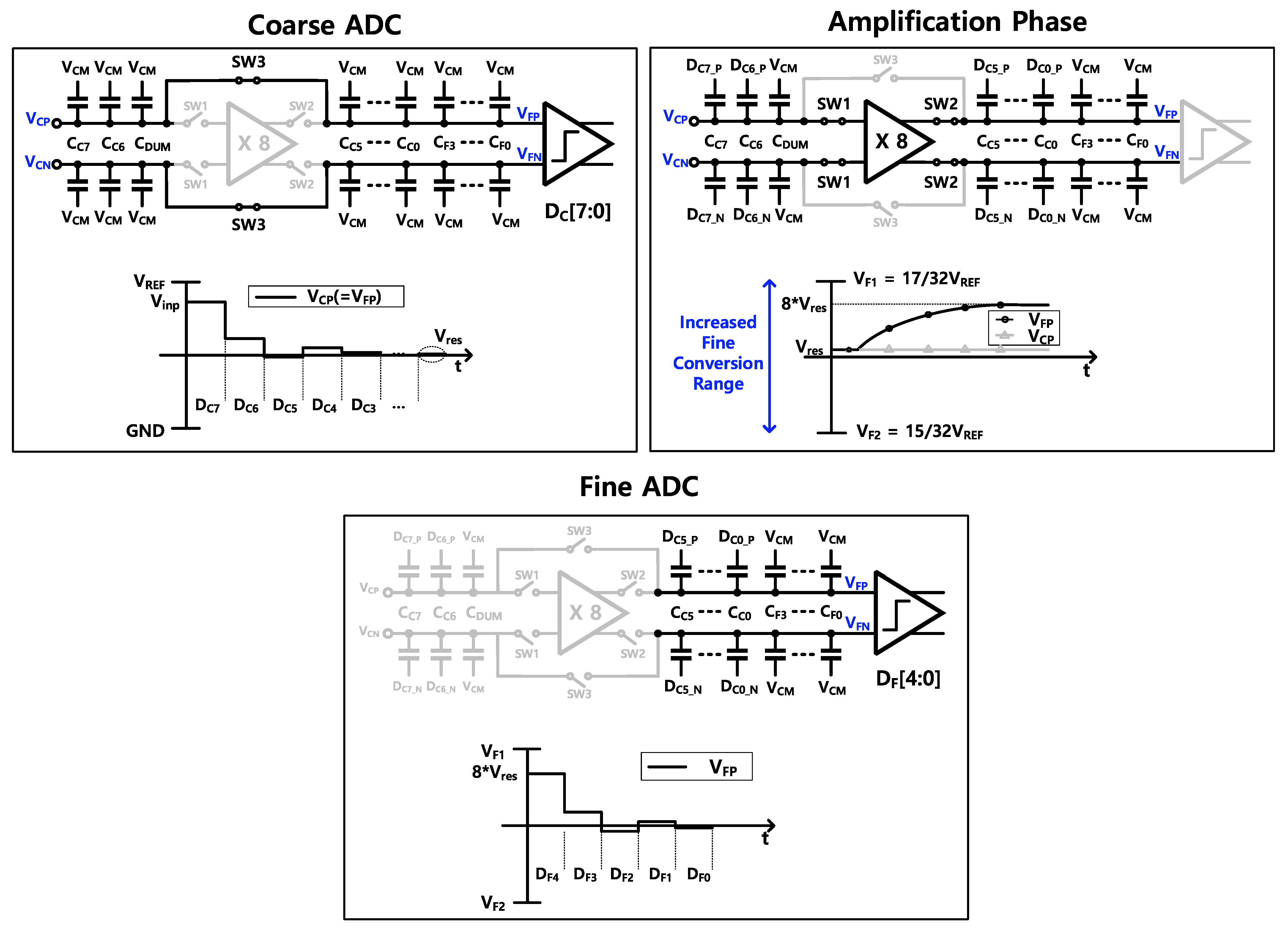
As shown in Figure 2, the operation of the proposed ADC can be divided into three phases. During the sampling phase, the top-plate node switch (SW3) is turned on. Once sampling is completed, the coarse SAR ADC begins converting the sampled analog input into an 8-bit digital code ( D C [7:0]) by V C M -based switching method. Capacitors C C 7 C C 0 are switched to V R E F or G N D according to the comparator decisions. The residue voltage ( V r e s ) remains at the top plate of the CDAC at the end of the coarse SAR conversion. In the next amplification phase, SW3 is turned off, thereby splitting the top-plate node into two distinct nodes: V C P , V C N (coarse) and V F P , V F N (fine). Simultaneously, switches SW1 and SW2 are also turned on, connecting V C P and V C N to the input of the amplifier ( V F P ) and V F N to its output. During the amplification phase, the residue voltage is amplified to 8 V r e s and appears at the V F P and V F N nodes. At this point, the bottom plates of the coarse CDAC capacitors ( C C 7 C C 0 ) have already been set to V R E F or G N D based on the coarse conversion results. The V F P and V F N nodes are redefined by the amplifier output voltage, regardless of the residual coarse conversion results previously present at these nodes. In conjunction with fine capacitor arrays, capacitors C C 5 C C 0 act as signal attenuators to match the reduced input range required for fine conversion. The amplified residue voltage is digitized into 5-bit digital codes ( D F [4:0]) through fine SAR conversion.
The final output code is obtained by digitally adding D C [7:0] and D F [4:0], including 1-bit inter-stage overlap to compensate for the decision error from the coarse stage. The overlap range is set to one coarse LSB of V F S , d i f f / 2 8 = 9.375 mV. This redundancy improves tolerance to deterministic errors such as the residue amplifier and comparator offset at the coarse stage. However, it does not remove random noise (e.g., amplifier and comparator thermal noise) or input-dependent errors such as charge injections of the sampling switches because these are not fixed inter-stage shifts and vary with time.
The ADC operates at a sampling rate of 10 MHz and uses an 80 MHz global clock, as shown in Figure 1b. Both coarse and fine SAR conversions are performed asynchronously, requiring one-fourth and one-eighth of the total clock period, respectively, as the coarse and fine conversions resolve to 8 bits and 5 bits, while the remaining half is allocated to the amplification phase. To increase the operation speed of the ADC, the amplification time could be reduced at the expense of increased power consumption.

2.2. Design Considerations

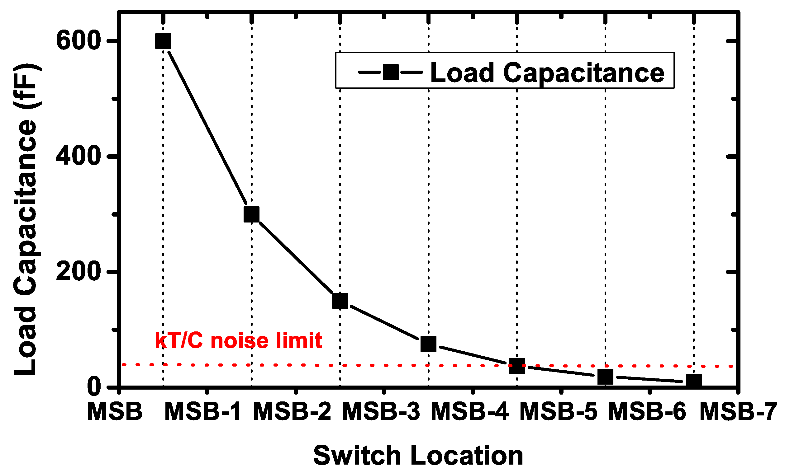
The load capacitance of the residue amplifier is determined by the location of the top-plate node switch (SW3) that splits the CDAC, which directly influences the amplifier’s power consumption. Therefore, optimal switch placement is essential to achieve an energy-efficient design. Figure 3 illustrates how the amplifier’s load capacitance varies with the switch position. As the switch moves toward the side of the least significant bit (LSB), the load capacitance decreases exponentially. While a smaller load is advantageous for minimizing amplifier power, it may degrade the signal-to-noise ratio (SNR) due to increased thermal noise (kT/C). Additionally, kickback noise from the comparator during the fine conversion phase can further limit SNR performance.
In this design, the top-plate node switch is placed between the MSB-1 and MSB-2 capacitors, representing a trade-off between power efficiency and noise immunity. If only kT/C noise is considered, the switch could alternatively be placed between MSB–2 and MSB–3 or between the MSB–3 and MSB–4 capacitors. However, during the fine conversion phase, a small top-plate capacitance increases the comparator’s kickback noise, as summarized in Table 1. Consequently, despite the higher amplifier load, the switch position is chosen to balance both thermal and kickback noise considerations, ensuring stable and accurate conversion.

2.3. Charge Injection Error Analysis

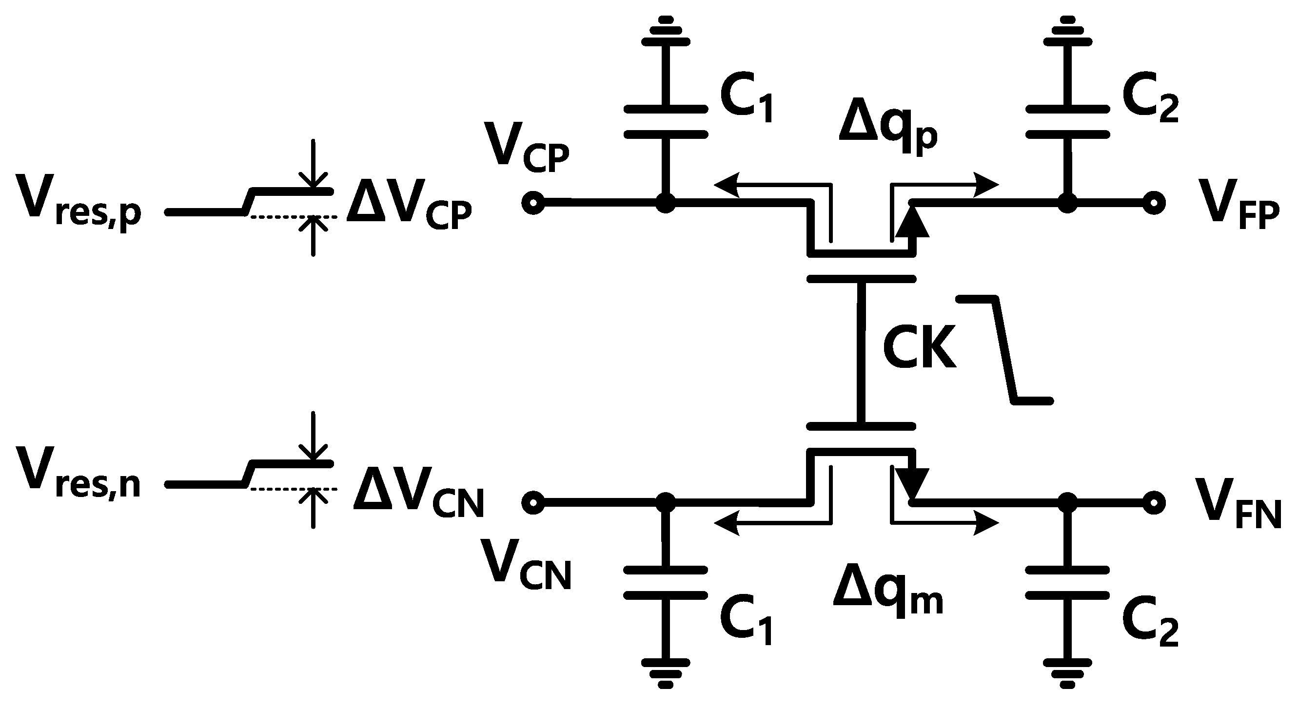
The splitting switch, i.e., the SW3 design, is the most critical component in the proposed design. SW3, together with the total CDAC capacitance, determines the overall bandwidth of the CDAC; therefore, it is implemented in a bootstrapped configuration to ensure constant on resistance. After the coarse conversion is completed, SW3 is turned off. At this point, charge injection introduces an error in the residue voltage, as illustrated in Figure 4. During the amplification phase, the V C P and V C N nodes serve as the input node of the residue amplifier. Therefore, the residue voltage at the V C P and V C N nodes must remain unaffected by the injection error, which is generated from the NMOS switch (SW3) after the coarse conversion. The charge injection error induced into the V F P and V F N nodes is not critical because the fine CDAC voltage is subsequently redefined by the amplifier output. The charge injection error on the positive side ( Δ q p ) can be expressed as,
Δ q p = W L C o x ( V C K V r e s , p V T H , p o s ) ,
where V C K and V T H , p o s are the voltage of the clock signal and the threshold voltage of the positive side switch, respectively. Since the injected charge is distributed between the drain and source nodes, the resulting voltage error at the V C P node ( Δ V C P ) is given by
Δ V C P = W L C o x V C K V r e s , p V T H , p o s 2 C 1 .
Since NMOS-bootstrapped switches are employed for SW3, the resulting charge injection error in the differential structure can be expressed as
Δ V C P Δ V C N = W L C o x ( V r e s , n V r e s , p ) + ( V T H , n e g V T H , p o s ) 2 C 1 .
The value of C 1 is the sum of the most significant bit (MSB), i.e., MSB-1, and dummy capacitances. In the proposed ADC, C 1 and W L C o x are set to 900 fF and 4 fF, respectively. Assuming there is no decision error in the coarse conversion, the maximum differential residue voltage is approximately 8 mV. Therefore, the differential charge injection error is limited to 35.5 μ V. Moreover, the maximum threshold voltage deviation occurs when the differential residue voltage reaches its peak. At this voltage difference, the threshold voltage mismatch between the differential switches is less than 250 μ V across all process corners. Although the residue voltage becomes four times greater than the LSB of the coarse ADC, the difference in threshold voltage remains below 1 mV. The resulting differential voltage error due to charge injection is less than 10 μ V, indicating the charge injection effect is negligible in this design.

3. Circuit Implementations

3.1. CDAC

The CDAC capacitor array is partitioned into coarse and fine sections. The coarse CDAC comprises an 8-bit binary-weighted array, while the fine CDAC consists of a 4-bit array. To eliminate gain mismatch between the two stages, a dummy capacitor ( C D u m ) is included in the coarse section. Its capacitance is designed to be three times larger than the total capacitance of the fine CDAC, which leads to a unit capacitance in the coarse CDAC that is twice that of the fine CDAC. Manually designed metal–oxide–metal (MOM) capacitors with M3 and M4 are used as unit elements throughout the unit capacitor array. The total capacitance of the ADC can be calculated by
C f i n e + C c o a r s e + C d u m = 16 C F 0 + 256 C C 0 + 48 C F 0 = 576 C F 0
Because the unit capacitance of the fine CDAC is 2 fF, the total capacitance of CDAC is approximately 1.2 pF for each differential side. When the conventional CDAC switching scheme is used, a total capacitance of 2 12 C u n i t is required to achieve 12-bit resolution. By adopting a V C M -based switching method, the required capacitance can be reduced to 2 11 C u n i t , corresponding to a 50% reduction compared with the conventional approach. In contrast, the proposed two-step scheme requires only 576 C u n i t , achieving a further 72% reduction compared to the V C M -based switching method in total capacitance, thereby substantially decreasing the chip area and improving power efficiency.

3.2. Residue Amplifier

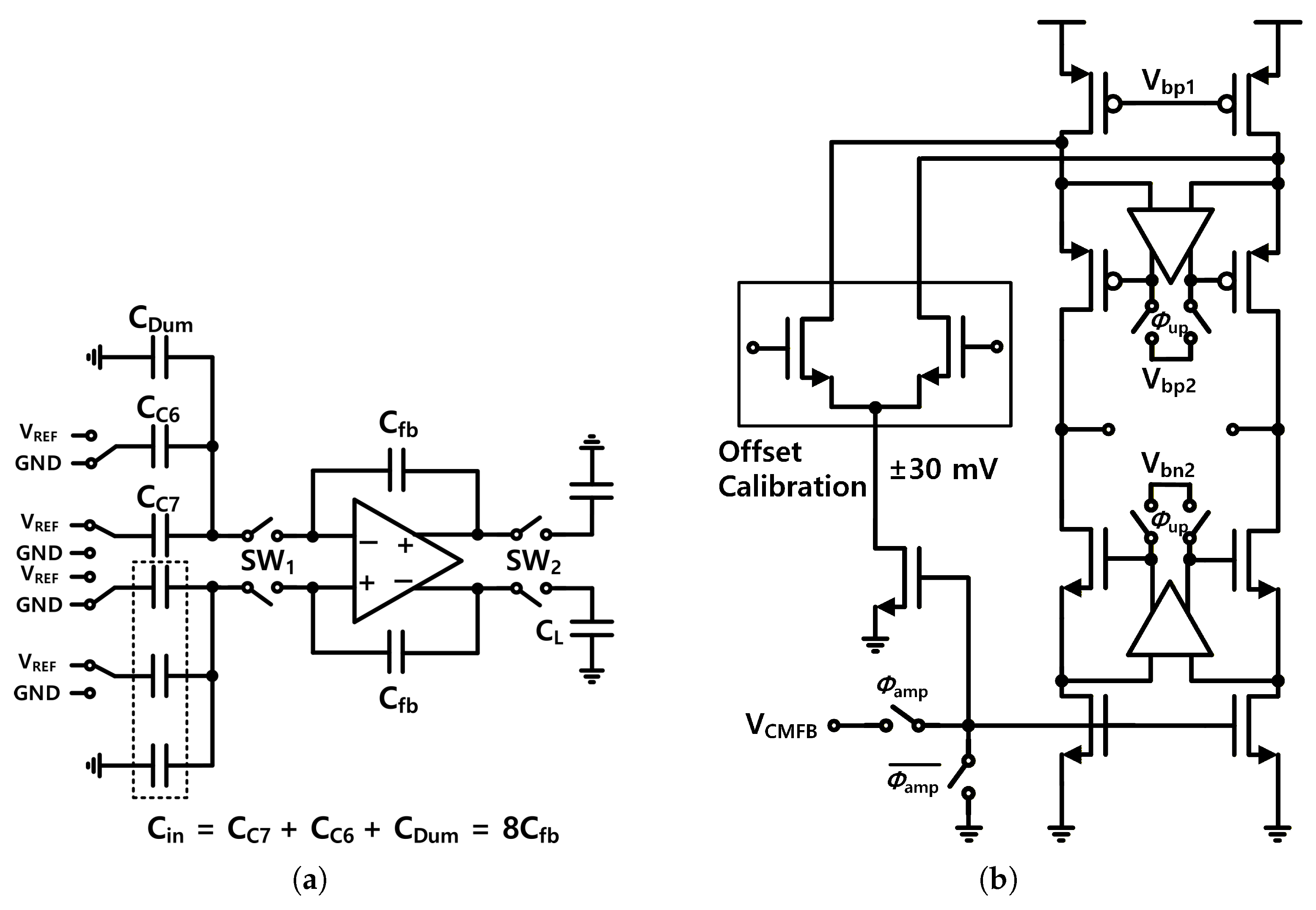
Figure 5a presents a detailed schematic of the structure of the residue amplifier. During the amplification phase, C C 7 , C C 6 , and C D u m serve as input sampling capacitors, while remaining CDAC capacitors act as load capacitors. As a result, the amplifier drives only one-fourth of the total capacitance of the CDAC, effectively mitigating power consumption concerns. The feedback capacitor ( C f b ) is designed to be one-eighth of the input capacitance ( C i n ), where C i n = C C 7 + C C 6 + C D u m , leading to a closed-loop gain of eight.
As presented in Figure 5b, a single-stage, folded-cascode amplifier with a gain-boosting structure is employed to ensure sufficient accuracy of the fine ADC. The boosting amplifier is also a fully differential, folded-cascode structure, which is a scaled version of main amplifier with a current ratio of 1/8. The amplifier is turned off during both the sampling and conversion phases using a switching op-amp technique [7] to further reduce power consumption. When the amplifier is turned off, the NMOS bias is pulled to ground. During the amplification phase, the boosting amplifier needs to recover from the off state. To shorten the start-up time, bias voltages V b n 2 and V b p 2 are temporarily connected to the boosting amplifier’s output during the amplifier start-up time, as described in Figure 1b. Since the amplification phase occupies 50% of the total ADC operation time, this technique results in a 50% reduction in amplifier power dissipation, achieving an open-loop gain of 56 dB and a unity-gain bandwidth of 90 MHz. Due to the finite open-loop gain, the amplifier introduces the closed-loop gain error. The closed-loop gain can be expressed as
A C L = C i n C f b · 1 1 + 1 A 0 ( 1 + C i n C f b )
where A 0 denotes the open-loop gain of the amplifier. Consequently, the normalized gain error can be approximated as
ϵ = 1 A 0 ( 1 + C i n C f b ) .
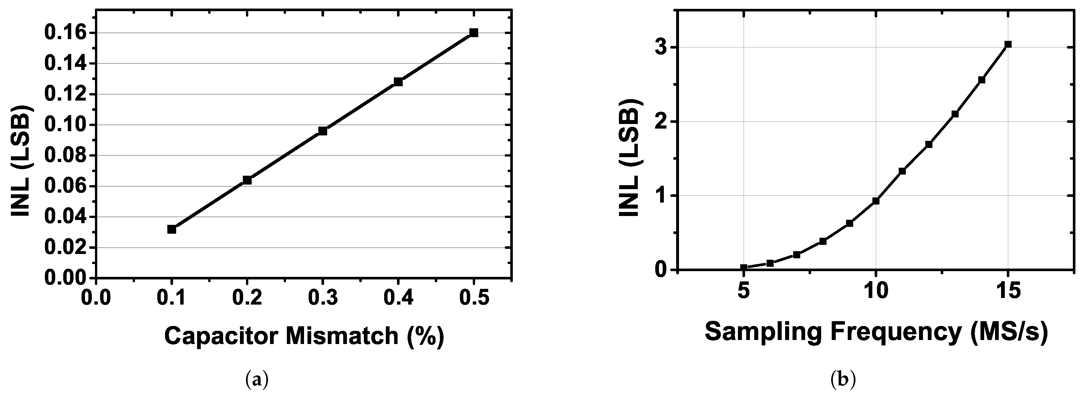
This gain error directly scales the residue voltage during the fine conversion phase and can therefore introduce non-linearity in the fine ADC. Considering a 5-bit conversion stage (i.e., 1 / 2 5 resolution), the integral non-linearity (INL) due to the finite amplifier gain is estimated to be 0.46 LSB. The mismatch between the input capacitance and feedback capacitance also leads to the gain error of the ADC, as expressed as (7). Figure 6a presents the resulting INL induced by the feedback capacitance mismatch. With an excessive mismatch variation of 0.5%, the INL reaches 0.16 LSB. Since the CDAC and feedback capacitors are implemented using manually designed MOM capacitors, it is not possible to either perform Monte Carlo simulations to evaluate nonlinearity or to directly refer to mismatch information provided by the process design kit (PDK). In the 65 nm CMOS process, 1 fF of the capacitor typically exhibits less than 1% mismatch. Therefore, with C f b = 60 fF, the expected mismatch is around 0.1%, which has a negligible effect on linearity.
The maximum achievable sampling frequency of the proposed ADC is primarily limited by the settling behavior of the residue amplifier between the coarse and fine conversion phases. As the sampling frequency increases, the available amplification time decreases proportionally. Consequently, insufficient settling of the residue voltage occurs, introducing an inter-stage gain error between the coarse and fine conversions. This gain error causes INL degradation. As shown in Figure 6b, we estimated the INL error assuming the amplifier to be an one-pole system. The proposed ADC can maintain an INL below 1 LSB at 12-bit resolution up to the sampling frequency of 10 MS/s. Beyond this frequency, the INL increases exponentially due to the limited settling time. Therefore, we consider 10 MS/s to be the practical upper bound of the current design. At higher sampling frequencies, the linearity degrades significantly.
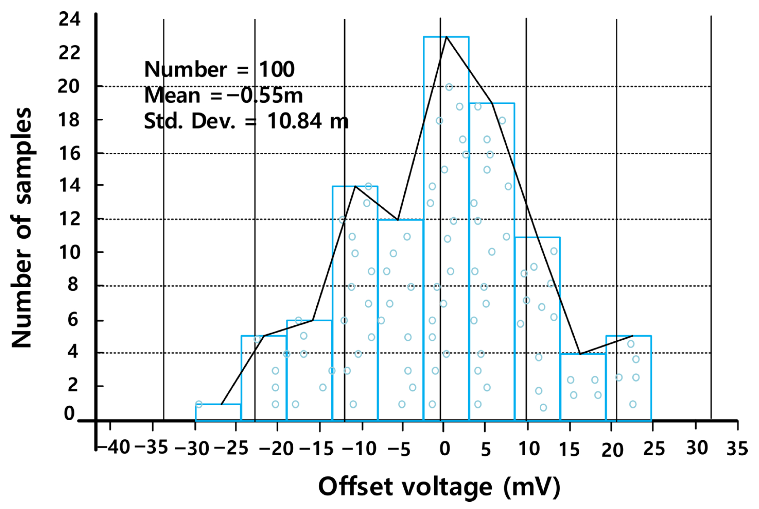
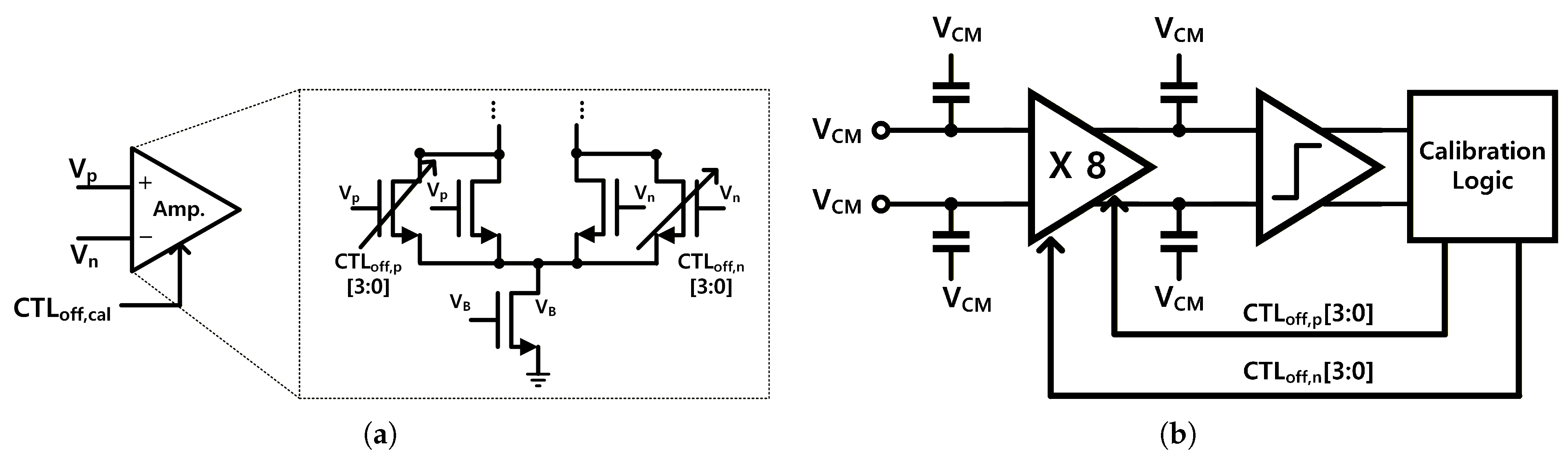
Redundancy between the coarse and fine stages is assigned to compensate for potential decision errors during coarse conversion. However, due to the high closed-loop gain, the amplifier offset can exceed the redundancy range. To address this, foreground offset calibration is applied to ensure the offset remains within the tolerable range. According to the Monte Carlo simulation results shown in Figure 7, the 3 σ input-referred offset value is 32.5 mV. Figure 8 shows the offset calibration circuit for the offset of the residue amplifier. As shown in Figure 8a, the calibration circuit utilizes binary-weighted input MOS pairs of the amplifier to effectively adjust the transconductance. The foreground calibration proceedsbefore the ADC start to convert the analog input signal. During calibration, the differential inputs are shorted together to the common-mode voltage, and the comparator determines which side of the transistor pair should be turned on. This procedure is carried out using a binary searching method as a 4-bit SAR ADC. With a resolution of 2 mV and a 4-bit control scheme, the calibration circuit is able to correct offset voltages from −30 mV to +30 mV.

3.3. Comparator

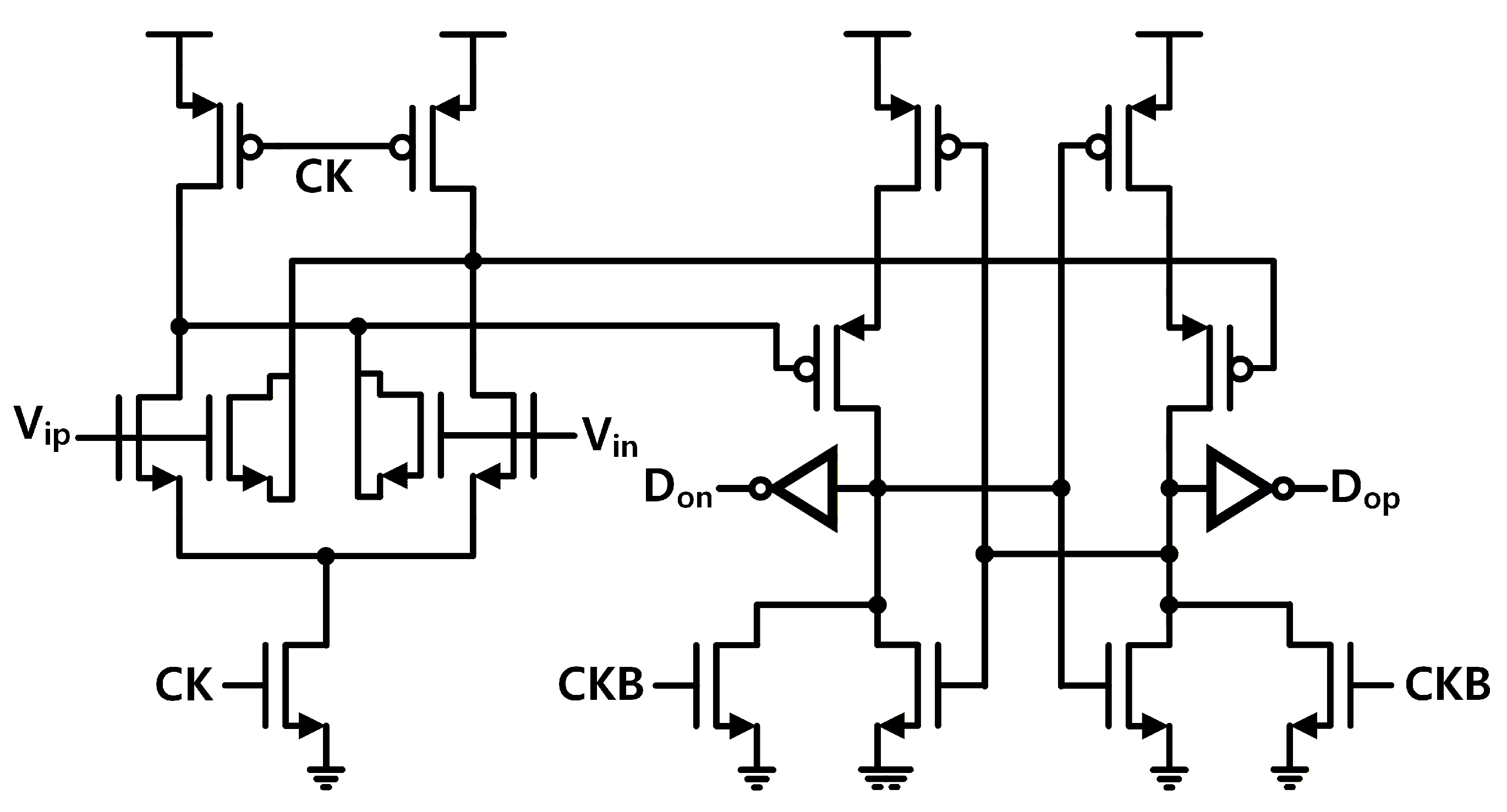
The proposed design enables a single-comparator implementation for two-step A/D conversion. The clocked comparator consists of a dynamic pre-amplifier followed by a latch stage. Figure 9 shows a schematic of the comparator. The employed cross-coupled dummy input transistors are sized identically to the of main input transistors in the pre-amplifier to suppress the kickback noise injected to the CDAC [17]. Since the fine conversion range is enlarged by a factor of eight, the comparator noise and offset requirement are also relaxed by an equivalent scale. The simulated input-referred noise of the comparator is 470 μ V r m s , which corresponds to one-fourth of the LSB voltage.

4. Measurement Results

After the layout design, the proposed ADC is simulated with extracted parasitic RC components for design verifications. The evaluated corners are three representative cases defined as SS (100 °C, 1.1 V), TT (27 °C, 1.2 V), and FF (0 °C, 1.3 V). Table 2 summarizes post-layout simulation results of the proposed ADC across PVT corners. The dynamic performance metrics were obtained at a sampling frequency of 10 MS/s with a Nyquist-rate input signal. At the SS corner, the SNDR decreases due to the increased transistor threshold voltage at the elevated temperature, while power consumption decreases primarily as a result of the reduced reference and supply voltage levels. The FF corner exhibits performance comparable to that of the TT corner; however, power consumption increases significantly, owing to the higher power supply voltage and reduced threshold voltage, which increase bias current under low-temperature conditions. In addition, supply-voltage variation was investigated to determine the minimum usable VDD. Below approximately 1.1 V, the residue amplifier cannot maintain proper biasing due to insufficient voltage headroom. As a result, the amplification stage fails to operate properly, causing incomplete settling and significant degradation of the fine-stage conversion accuracy.
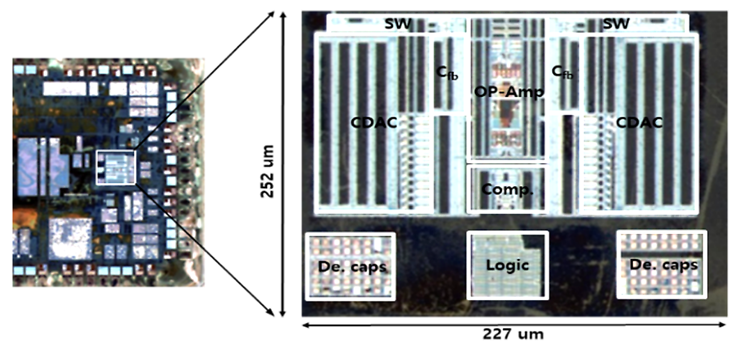
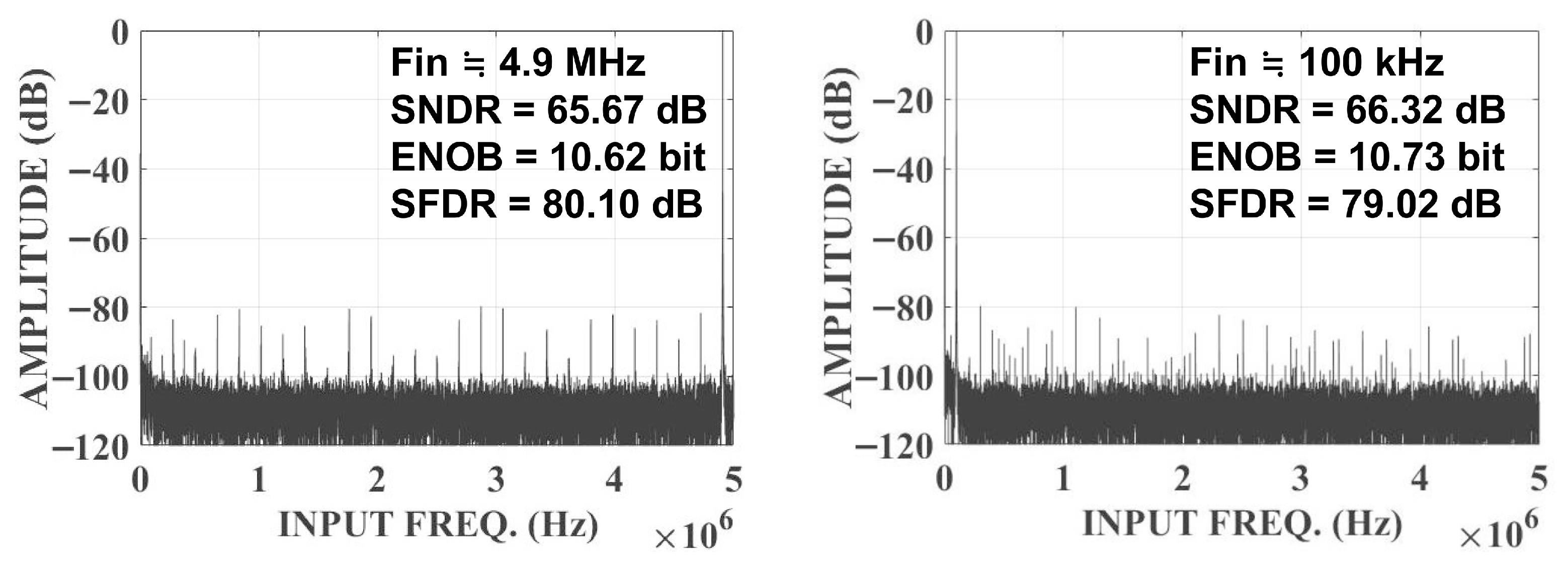
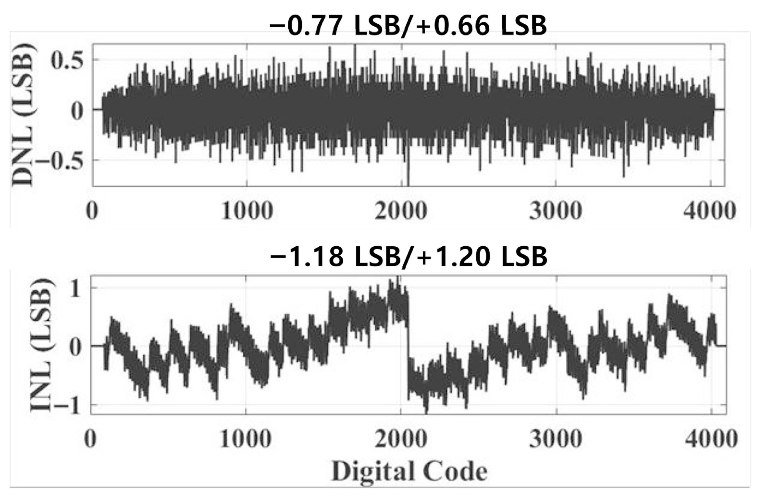
A prototype chip was fabricated using 65 nm CMOS technology, occupying an active area of 252 μ m × 227 μ m, as shown in Figure 10. All measurement results were obtained after performing the amplifier foreground calibration described in Section 3.2. The dynamic performance was evaluated using a 16,384-point fast Fourier transform (FFT) at a sampling rate of 10 MS/s with a peak-to-peak input voltage of 0.96 V. As shown in Figure 11, the proposed ADC achieves SNDRs of 66.32 and 65.67 dB and spurious free dynamic ranges (SFDRs) of 79.02 and 80.10 dB for slow (100 kHz) and Nyquist-rate input frequencies, respectively. The static performance shown in Figure 12 was characterized using a histogram method. The measured differential nonlinearity (DNL) and INL are +0.66 LSB/−0.77 LSB and +1.2 LSB/−1.18 LSB. The excessive INL results from the capacitor mismatch of the custom-designed MOM capacitor used in the CDAC. However, the use of such small unit capacitors enables a significant reduction in chip area and power consumption.
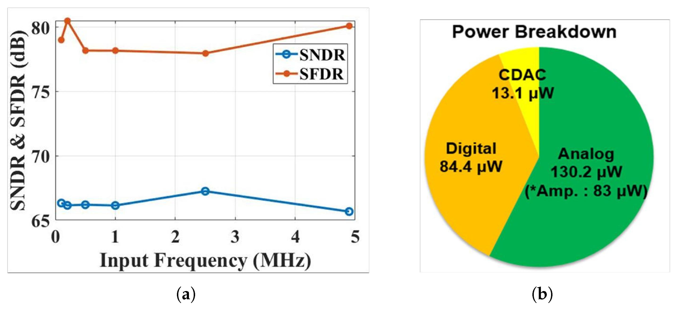
Figure 13 presents the SNDR and SFDR versus the input frequency, along with the power breakdown. The SNDR at the Nyquist rate degrades by less than 1 dB, indicating that the effective resolution bandwidth (ERBW) exceeds the Nyquist frequency. The peak SNDR reaches 67.25 dB at an input frequency of approximately 2.5 MHz.
The total power consumption of the proposed ADC is 227.7 μ W under a 1.2 V supply. The analog power includes the consumption of the residue amplifier, comparator, and switching circuits. Specifically, the amplifier consumes 83 μ W, which accounts for 64% of the total analog power. Although the proposed amplifier consumes the most power among the ADC building blocks, a reduction in CDAC capacitance greatly reduces power consumption. The resulting FoM is 14.5 fJ/conversion step.
A performance summary and comparison with state-of-the-art ADCs operating at sampling rates below 100 MS/s are provided in Table 3. Despite the use of an analog op-amp in the residue amplification stage, the proposed ADC demonstrates competitive energy efficiency.

5. Conclusions

This paper presents a two-step sub-ranging SAR ADC architecture that enables two-step operation without requiring a multi-stage design. By dividing the sampling node, the load capacitance of the residue amplifier is significantly reduced, and the CDAC capacitance is reduced by 86%. This allows the ADC to achieve high energy efficiency while maintaining an effective number of bits (ENOB) greater than 10. A prototype chip was fabricated using 65 nm CMOS technology and achieved an SNDR of 65.7 dB at a Nyquist-rate input. The corresponding Walden FoM is 14.5 fJ/conversion step, demonstrating the competitiveness of the proposed architecture.

Author Contributions

Conceptualization, J.S.; methodology, J.S.; software, J.S.; validation, J.S.; formal analysis, J.S. and C.L.; investigation, J.S. and C.L.; resources, J.S. and C.L.; data curation, J.S. and C.L.; writing—original draft preparation, J.S.; writing—review and editing, J.S. and C.L.; visualization, J.S. and C.L.; supervision, C.L.; project administration, C.L.; funding acquisition, C.L. All authors have read and agreed to the published version of the manuscript.

Funding

This work was supported by the Hankuk University of Foreign Studies Research Fund of 2026.

Data Availability Statement

All the data are reported/cited in the paper.

Acknowledgments

Fabrication of the chip fabrication EDA tool was supported by the IC Design Education Center (IDEC), Republic of Korea.

Conflicts of Interest

Author Jaegeun Song was employed by the company Samsung Electronics. The remaining authors declare that the research was conducted in the absence of any commercial or financial relationships that could be construed as a potential conflict of interest.

References

  1. Zhu, Y.; Chan, C.H.; Chio, U.-F.; Sin, S.W.; Seng-Pan, U.; Martins, R.P.; Maloberti, F. A 10-bit 100-MS/s reference-free SAR ADC in 90 nm CMOS. IEEE J. Solid-State Circuits 2010, 45, 1111–1121. [Google Scholar] [CrossRef]
  2. Bae, S.; Lee, S.; Seong, S.; Kong, S.; Park, B.; Lee, M. A 13-Bit 1-MS/s SAR ADC with Completion-Aware Background Capacitor Mismatch Calibration. IEEE Access 2023, 11, 104323–104332. [Google Scholar] [CrossRef]
  3. Song, J.; Park, Y.; Lim, C.; Choi, Y.; Ahn, S.; Park, S.; Kim, C. A 9-bit 500-MS/s 2-bit/cycle SAR ADC with error tolerant interpolation technique. IEEE J. Solid-State Circuits 2022, 57, 1492–1503. [Google Scholar] [CrossRef]
  4. Zhu, Y.; Chan, C.-H.; Chio, U.-F.; Sin, S.-W.; U, S.-P.; Martins, R.P.; Maloberti, F. Split-SAR ADCs: Improved linearity with power and speed optimization. IEEE Trans. Very Large Scale Integr. (VLSI) Syst. 2014, 22, 372–383. [Google Scholar] [CrossRef]
  5. Wang, X.; Li, F.; Wang, Z. A simple histogram-based capacitor mismatch calibration in SAR ADCs. IEEE Trans. Circuits Syst. II Exp. Briefs 2020, 12, 2838–2842. [Google Scholar] [CrossRef]
  6. Nuzzo, P.; Bernardinis, F.D.; Terreni, P.; der Plas, G.V. Noise analysis of regenerative comparators for reconfigurable ADC architectures. IEEE Trans. Circuits Syst. I Reg. Pap. 2008, 55, 1441–1454. [Google Scholar] [CrossRef]
  7. Furuta, M.; Nozawa, M.; Itakura, T. A 10-bit, 40-MS/s, 1.21 mW pipelined SAR ADC using single-ended 1.5-bit/cycle conversion technique. IEEE J. Solid-State Circuits 2011, 46, 1360–1370. [Google Scholar] [CrossRef]
  8. van der Goes, F.; Ward, C.M.; Astgimath, S.; Yan, H.; Riley, J.; Zeng, Z.; Mulder, J.; Wang, S.; Bult, K. A 1.5 mW 68 dB SNDR 80 Ms/s 2 × interleaved pipelined SAR ADC in 28 nm CMOS. IEEE J. Solid-State Circuits 2014, 49, 2835–3845. [Google Scholar] [CrossRef]
  9. Gandara, M.; Guo, W.; Tang, X.; Chen, L.; Yoon, Y.; Sun, N. A pipelined SAR ADC reusing the comparator as residue amplifier. In Proceedings of the 2017 IEEE Custom Integrated Circuits Conference (CICC), Austin, TX, USA, 30 April–3 May 2017; pp. 1–4. [Google Scholar]
  10. Harpe, P.; Cantatore, E.; van Roermund, A. A 10 b/12 b 40 kS/s SAR ADC with data-driven noise reduction achieving up to 10.1 b ENOB at 2.2 fJ/conversion-step. IEEE J. Solid-State Circuits 2013, 48, 3011–3018. [Google Scholar] [CrossRef]
  11. Chen, L.; Tang, X.; Sanyal, A.; Yoon, Y.; Cong, J.; Sun, N. A 0.7-V 0.6-μW 100-kS/s low-power SAR ADC with statistical estimation-based noise reduction. IEEE J. Solid-State Circuits 2017, 52, 1388–1398. [Google Scholar] [CrossRef]
  12. Zhang, J.; Ren, X.; Liu, S.; Chan, C.-H.; Zhu, Z. An 11-bit 100-MS/s pipelined-SAR ADC reusing PVT-stabilized dynamic comparator in 65-nm CMOS. IEEE Trans. Circuits Syst. II 2020, 67, 1174–1178. [Google Scholar] [CrossRef]
  13. Mao, A.; Mo, S.; Cai, Z. A low-power cyclic ADC with capacitive degeneration amplifier and charge mode operation. In Proceedings of the 2025 IEEE International Symposium on Circuits and Systems (ISCAS), London, UK, 25–28 May 2025. [Google Scholar]
  14. Ginsburg, B.P.; Chandrakasan, A.P. An energy-efficient charge recycling approach for a SAR converter with capacitive DAC. In Proceedings of the 2005 IEEE International Symposium on Circuits and System, Kobe, Japan, 23–26 May 2005; pp. 184–187. [Google Scholar]
  15. Liu, C.-C.; Chang, S.-J.; Huang, G.-Y.; Lin, Y.-Z. A 10-bit 50-MS/s SAR ADC with a monotonic capacitor switching procedure. IEEE J. Solid-State Circuits 2010, 45, 731–740. [Google Scholar] [CrossRef]
  16. Van Elzakker, M.; van Tuijl, E.; Geraedts, P.; Schinkel, D.; Klumperink, E.A.; Nauta, B. A 10-bit charge-redistribution ADC consuming 1.9 μW at 1 MS/s. IEEE J. Solid-State Circuits 2010, 45, 1007–1015. [Google Scholar] [CrossRef]
  17. Figueiredo, P.M.; Vital, J.C. Kickback noise reduction techniques for CMOS latched comparators. IEEE Trans. Circuits Syst. II 2006, 53, 541–545. [Google Scholar] [CrossRef]
  18. Liang, Y.; Song, S.; Zhu, Z. An 8-to-12-bit resolution-reconfigurable SAR ADC with fast-window-switching technique. IEEE Trans. Circuits Syst. II 2025, 72, 544–548. [Google Scholar] [CrossRef]
  19. Kwon, Y.; Kim, T.; Sun, N.; Chae, Y. A 348-μW 68.8-dB SNDR 20-MS/s pipelined SAR ADC with a closed-loop two-stage dynamic amplifier. IEEE Solid-State Circuits Lett. 2021, 4, 166–169. [Google Scholar] [CrossRef]
  20. Chung, Y.-H.; Zeng, Q.F.; Lin, Y.-S. A 12-bit SAR ADC with a DAC-configurable window switching scheme. IEEE Trans. Circuits Syst. I 2020, 67, 358–368. [Google Scholar] [CrossRef]
Figure 1. (a) Structure of the proposed SAR ADC; (b) timing diagram.
Electronics 15 01050 g001
Figure 2. Operational phases of the proposed ADC.
Electronics 15 01050 g002
Figure 3. Load capacitance of the amplifier according to switch location.
Electronics 15 01050 g003
Figure 4. Charge injection error at the division of the top-plate node.
Electronics 15 01050 g004
Figure 5. Structure of the (a) residue amplifier; (b) op-amp with offset calibration.
Electronics 15 01050 g005
Figure 6. INL error as a function of (a) residue amplifier feedback capacitance mismatch; (b) sampling frequency.
Electronics 15 01050 g006
Figure 7. Histogram of the offset voltage of the residue amplifier under Monte-Carlo simulations.
Electronics 15 01050 g007
Figure 8. (a) Offset correction circuit of the residue amplifier. (b) Foreground calibration engine.
Electronics 15 01050 g008
Figure 9. Schematic of the comparator with a pre-amplifier.
Electronics 15 01050 g009
Figure 10. Chip photograph.
Electronics 15 01050 g010
Figure 11. Measured dynamic performance of the proposed ADC.
Electronics 15 01050 g011
Figure 12. Measured INL and DNL.
Electronics 15 01050 g012
Figure 13. (a) SNDR and SFDR versus the input frequency. (b) Power breakdown.
Electronics 15 01050 g013
Table 1. Kickback and kT/C noise summary.
Switch LocationkT/C Noise [ mV rms ]Max. Kickback Noise [mV]
Between MSB-1 and MSB-20.1661.01 (=0.25 LSB)
Between MSB-2 and MSB-30.2351.85 (=0.45 LSB)
Between MSB-3 and MSB-40.3323.21 (=0.8 LSB)
Table 2. The post-layout simulation result of the proposed ADC under PVT corners.
SS, 100 °C, 1.1 VTT, 27 °C, 1.2 VFF, 0 °C, 1.3 V
SNDR (dB)63.867.766.5
SFDR (dB)81.285.978.3
ENOB (bit)10.3110.9510.75
Power ( μ W)169.7192.0215.4
Table 3. Performance comparison.
TCAS-II 2020 [12]TCAS-II 2025 [18]SSCL 2021 [19]TCAS-I 2020 [20]This Work
StructurePipelined-SARSARPipelined-SARSARTwo-step SAR
Tech. (nm)651806518065
Resolution1112131212
Supply (V)1.21.81.21.51.2
Fs (MS/s)10010202010
DNL (LSB)0.91-1.020.650.77
INL (LSB)1.01-2.281.061.2
ENOB * (bit)9.810.610.99.510.6
SNDR (dB)60.765.567.159.165.7
SFDR (dB)70.579.677.68180.1
Power ( μ W)2120583481220227.7
FoM ** (fJ/conv.)24.137.69.48314.5
Area (mm2)0.170.230.0650.10.057
* ENOB = (SNDR − 1.76)/6.02; ** FoM = Power/ F s 2 E N O B .
Disclaimer/Publisher’s Note: The statements, opinions and data contained in all publications are solely those of the individual author(s) and contributor(s) and not of MDPI and/or the editor(s). MDPI and/or the editor(s) disclaim responsibility for any injury to people or property resulting from any ideas, methods, instructions or products referred to in the content.