Article

Efficient Interleaver Architecture for Modern Global Navigation Satellite Systems

1
Launch Vehicle System Engineering & Integration Team, Korea Aerospace Research Institute, Daejeon 34133, Republic of Korea
2
Department of Electronics, Chungnam National University, Daejeon 34134, Republic of Korea
3
KPS User Segment Development Team, Korea Aerospace Research Institute, Daejeon 34133, Republic of Korea
4
Satellite Systems Laboratory, LIG Nex1, Seongnam 13488, Republic of Korea
*
Author to whom correspondence should be addressed.
Electronics 2026, 15(3), 526; https://doi.org/10.3390/electronics15030526
Submission received: 31 December 2025 / Revised: 18 January 2026 / Accepted: 22 January 2026 / Published: 26 January 2026

Abstract

In modern Global Navigation Satellite Systems (GNSS), interleavers are essential for improving system performance. However, limited research has focused on interleaver hardware optimization specifically for GNSS, primarily due to GNSS authorities strictly adhering to Interface Control Documents (ICDs), which discourage significant deviations in hardware implementations. Traditional GNSS interleavers employ double buffering and typically require extensive hardware resources, specifically 2N registers and 2(N 1) + 1 multiplexers (MUXs), leading to increased complexity, power consumption, and latency. To bridge this gap, this paper presents a novel and efficient interleaver hardware architecture optimized specifically for modern GNSS by leveraging Lifetime Analysis and Forward–Backward Register Allocation. Lifetime Analysis precisely identifies the minimum number of registers necessary, and Forward–Backward Register Allocation ensures efficient utilization of these resources under continuous operation. Experiments were conducted for all seven currently used GNSS interleaving configurations. Synthesis results, obtained using a standard 28 nm Complementary Metal-Oxide Semiconductor (CMOS) process, demonstrate significant reductions in chip area (38.82% reduction), power consumption (52.01% reduction), and latency (25.05% improvement) compared to conventional architectures. These benefits become increasingly critical as the interleaver data length N continues to grow, providing a practical, ICD-compliant solution for resource-constrained satellite payloads and receiver designs.

1. Introduction

Global Navigation Satellite Systems (GNSS) are essential infrastructures that provide positioning, navigation, and timing (PNT) services, crucial for various modern applications, including transportation, telecommunications, and national security [1]. Initially introduced through the Global Positioning System (GPS) by the United States in 1978, GNSS technology has significantly evolved, expanding globally with systems such as Russian GLONASS, European Galileo, Chinese BeiDou Navigation Satellite System (BDS), Japanese Quasi-Zenith Satellite System (QZSS), and Indian Navigation with Indian Constellation (NavIC) [2]. Among these, QZSS and NavIC are Regional Navigation Satellite Systems (RNSS), designed to provide regional coverage optimized for their respective service areas. Additionally, BDS has expanded from regional to global coverage. Early GNSS, such as GPS L1 C/A and GLONASS L1OF, provided fundamental navigation services using simple data structures with minimal error correction capabilities [3,4]. However, as GNSS services expanded globally and their applications became increasingly critical, the demand for enhanced reliability and data integrity significantly increased. To address these evolving needs, modern GNSS signals have adopted more sophisticated signal structures and advanced error-correcting techniques. For example, early GNSS signals like GPS L1 C/A employed basic error-correction algorithms such as Cyclic Redundancy Check (CRC) and Bose–Chaudhuri–Hocquenghem (BCH) codes, which can only correct a limited number of bit errors. In contrast, modern GNSS signals incorporate advanced methods such as Low-Density Parity-Check (LDPC) codes, offering significantly superior error-correcting capabilities, and symbol-based Reed–Solomon (RS) codes [5].
Moreover, combining interleaving with Forward Error Correction (FEC) significantly enhances error-correcting performance [6]. Interleaving is an effective technique used in communication systems to mitigate burst errors by rearranging encoded data, thus converting burst errors into random errors, which are more effectively corrected by FEC algorithms [7]. Recently developed GNSS signals increasingly adopt interleavers to enhance data reliability and system robustness. Table 1 summarizes the interleaver adoption status in major GNSS signals, highlighting the transition from early systems without interleaving to modern GNSS signals extensively employing interleavers. As indicated in Table 1, modern GNSS signals significantly incorporate interleavers, emphasizing the importance of robust error correction and improved signal integrity.
Many studies have addressed interleaver optimization in communication systems, such as 4G Long-Term Evolution (LTE) and 5G New Radio (NR), to enhance hardware efficiency in terms of area, power consumption, and latency [24,25,26,27,28]. However, limited research has focused on interleaver hardware optimization specifically for GNSS, primarily due to GNSS authorities strictly adhering to Interface Control Documents (ICDs), thus discouraging significant deviations in hardware implementations. Due to stringent requirements for power efficiency, low complexity, and compact hardware implementation, GNSS urgently require efficient hardware design solutions [29,30,31]. To bridge this gap, this paper presents a novel and efficient interleaver hardware specifically developed for modern GNSS constellations. An innovative architecture is proposed utilizing two powerful Very-Large-Scale Integration (VLSI) optimization techniques: Lifetime Analysis and Forward–Backward Register Allocation. We implement both conventional and proposed architectures for all interleaver sizes listed in Table 1 and demonstrate significant reductions in hardware complexity, area, power consumption, and latency. The proposed interleaver architecture offers practical advantages for both satellite payloads and GNSS receivers and is suitable for existing GNSS constellations as well as emerging navigation systems [32].
The remainder of this paper is organized as follows. Section 2 presents the theoretical background and analyzes conventional GNSS interleaver structures. Then, Section 3 introduces the proposed optimization methodology and describes the novel interleaver architecture. Section 4 presents experimental results comparing the proposed architecture against conventional designs. Finally, Section 5 concludes the paper and summarizes the key contributions.

2. Background

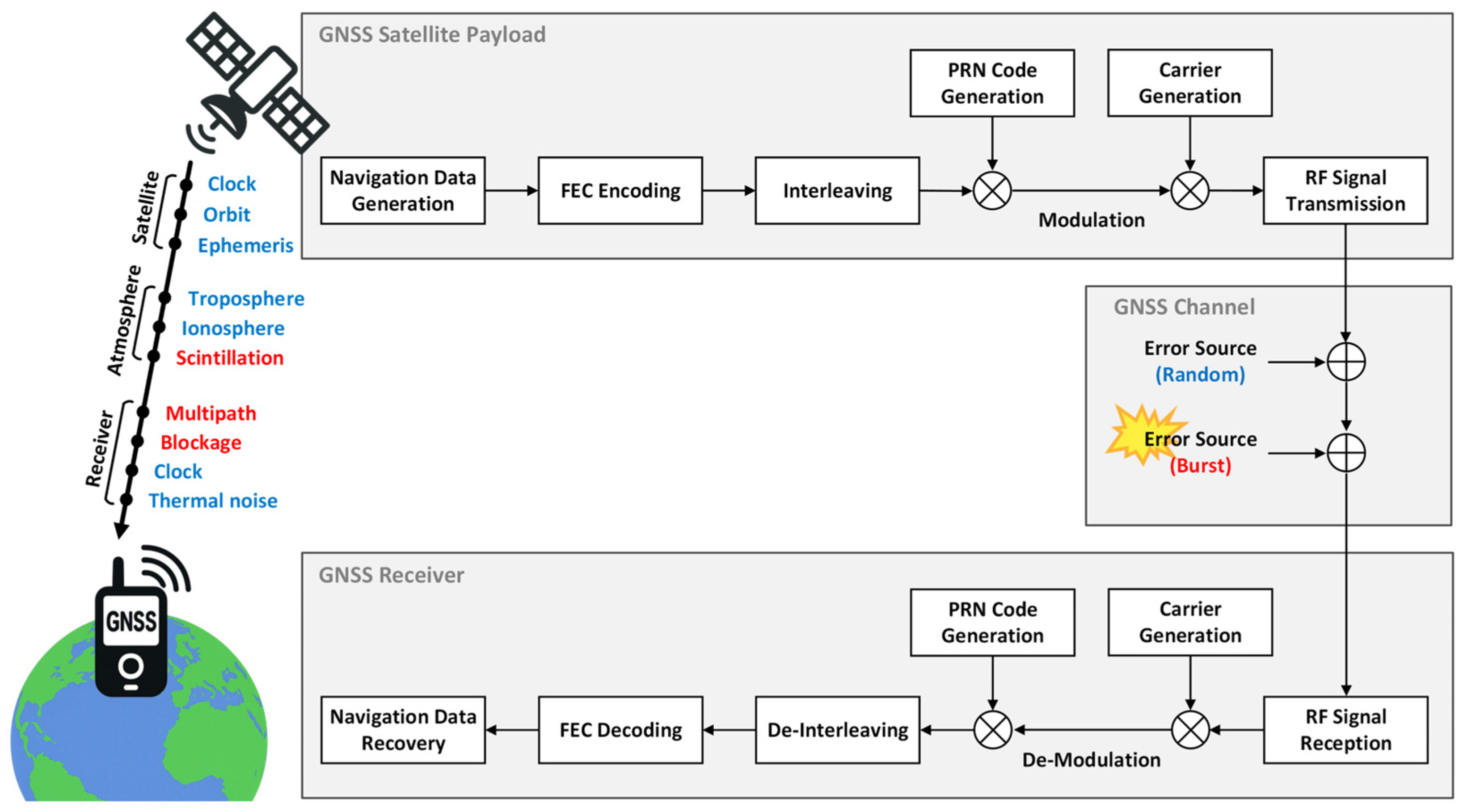
GNSS transmits PNT data from satellites to terrestrial receivers through structured signal processing stages, as depicted in Figure 1 [33]. In modern satellite payloads, navigation data are encoded using FEC techniques to ensure robust data integrity during transmission. Subsequently, the encoded data undergo interleaving, rearranging bits across multiple frames to enhance error correction capability. The interleaved bits are then modulated, converting digital data into suitable radio frequency (RF) signals for reliable transmission. In contrast, incoming signals at the receiver front end undergo a reverse sequence of processing steps. The received signals are demodulated, deinterleaved, and decoded using FEC algorithms to correct transmission errors and restore accurate navigation data.
During transmission channels from satellites to terrestrial receivers, GNSS signals typically encounter two primary types of errors: random errors and burst errors. Random errors occur sporadically and are primarily attributed to clock errors, orbital errors, ephemeris inaccuracies, tropospheric delays, ionospheric delays, receiver clock instabilities, and thermal noise. Conversely, burst errors affect consecutive bits and are generally caused by ionospheric scintillation, multipath effects, and signal blockage [1]. To handle these errors, FEC techniques are typically employed, with their error-correction capability defined based on fixed-length data frames. For example, a BCH (n, k, t) code encodes a k-bit message into an n-bit codeword, enabling correction of up to t bit errors per codeword. However, despite these measures, burst errors can often surpass the correction capability of standard FEC codes, especially when multiple consecutive errors occur within a single frame, potentially causing critical decoding failures [34].
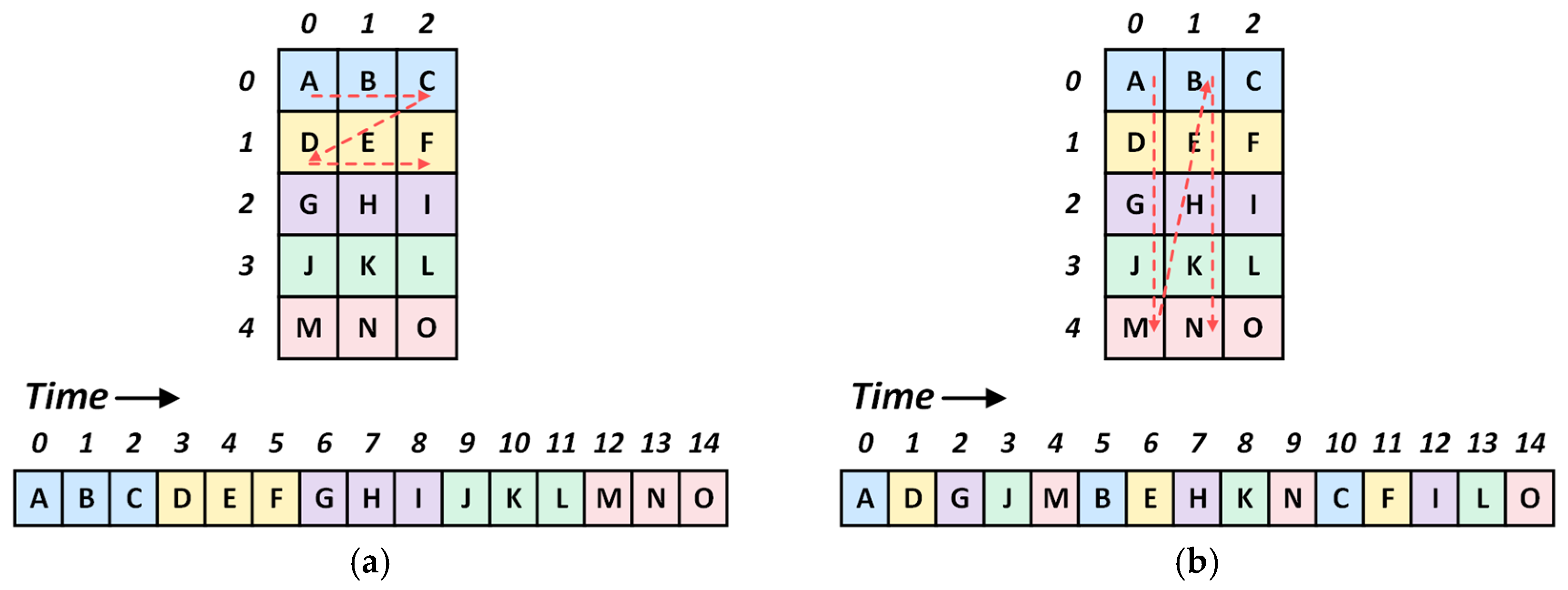
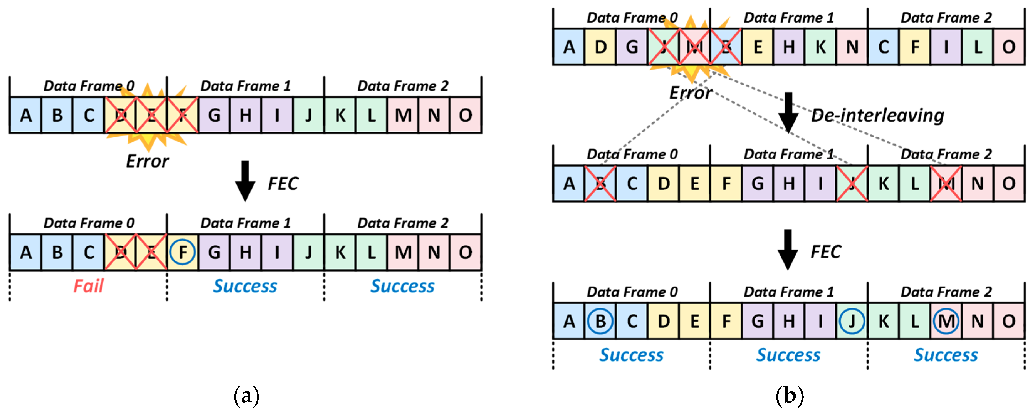
To enhance robustness against burst errors, interleaving is commonly employed in modern GNSS as a data rearrangement technique [35]. It redistributes encoded bits across multiple frames, transforming burst errors into random-like errors manageable by FEC. Figure 2 illustrates the operation of an N R × N C block interleaver, where N R and N C represent the number of rows and columns, respectively. Data bits are typically filled into this interleaver matrix column-wise and read out row-wise, or vice versa. This rearrangement disperses consecutive bits across separate frames, ensuring burst errors encountered during transmission are distributed across multiple code words. For instance, Figure 3 illustrates an FEC scheme capable of correcting 1 bit error per 5-bit frame combined with a 5 × 3 block interleaver structure. Without interleaving, as shown in Figure 3a, a burst error concentrated within a single frame can exceed the FEC correction capability, leading to decoding failures. In contrast, Figure 3b illustrates that with interleaving, burst errors are effectively distributed across multiple frames, enabling each frame to remain within the correction limits of the FEC. At the receiver, a deinterleaver restores the interleaved data stream to its original order by performing the inverse index mapping of the block interleaver. Since interleaving and deinterleaving form a mathematically symmetric pair, the same optimization framework can be applied by constructing an allocation schedule for the inverse mapping. Through this transmit-receive rearrangement process, burst errors are dispersed across multiple frames, thereby creating conditions under which FEC can correct errors more effectively.
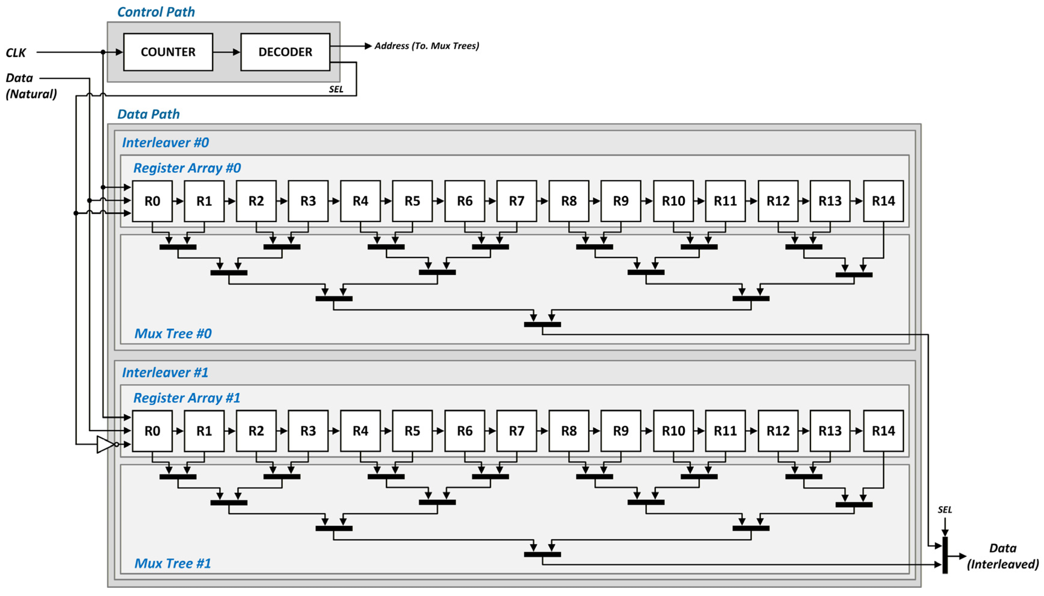
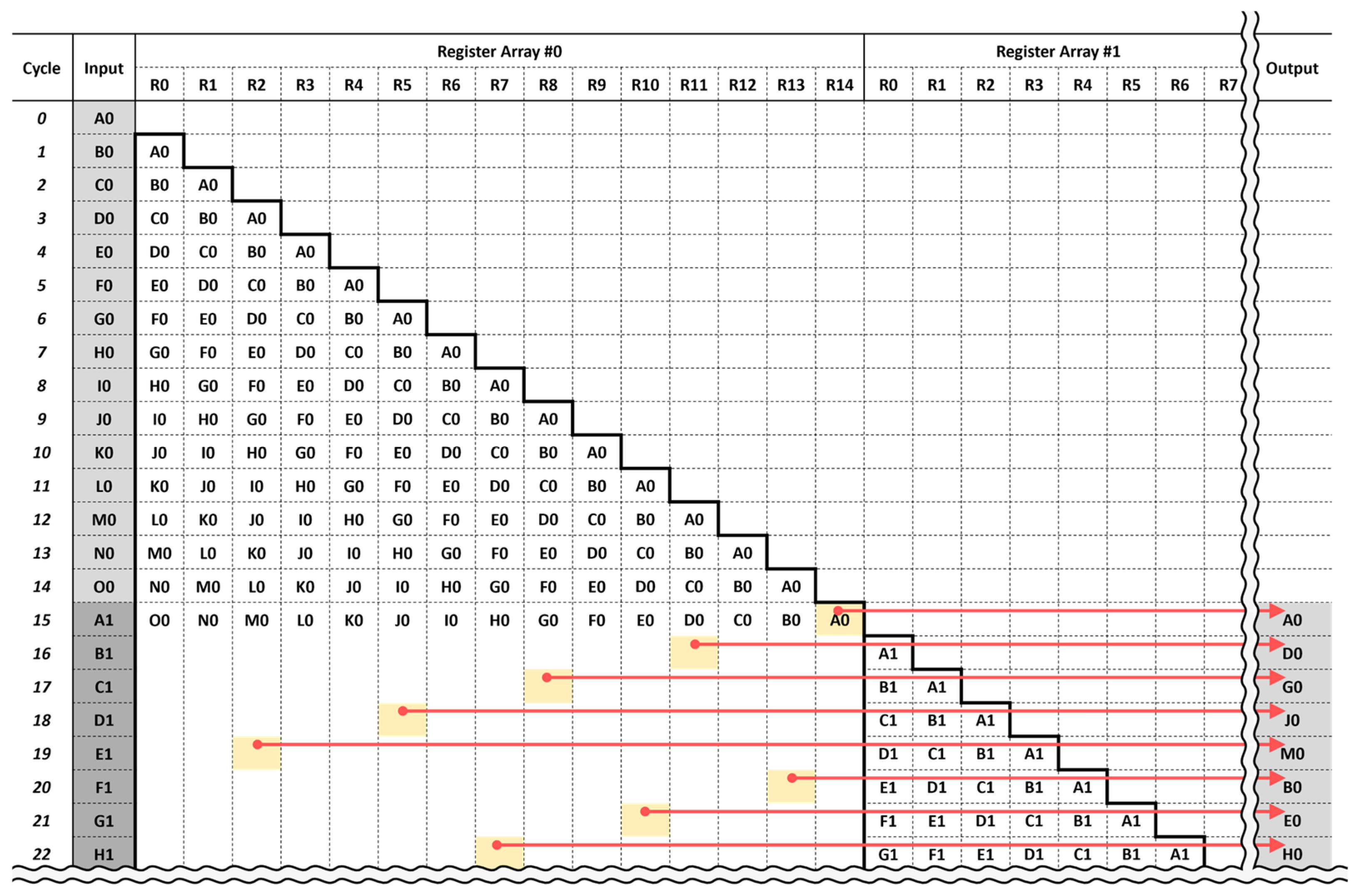
Thus, interleaving significantly enhances the effectiveness of FEC algorithms, improving the reliability and accuracy of GNSS data recovery, particularly in environments susceptible to burst errors. In addition, Figure 4 illustrates a typical 5 × 3 interleaver architecture consisting of 2N registers, 2(N 1) + 1 multiplexers (MUXs), and dedicated control logic, where N = N R × N C [36]. During the write operation, input data bits are sequentially stored in registers following normal order. Conversely, during the read operation, data bits are retrieved from these registers in an interleaved sequence predetermined by the N R × N C interleaving matrix, as depicted in Figure 2. The associated control logic manages this read–write sequence by generating appropriate control signals, allowing the MUX tree to select the required data bit from among N registers. Furthermore, a double buffering scheme is crucial to prevent data collisions and ensure continuous operation in this conventional interleaver structure. Specifically, while one register array is being filled with incoming data in normal order, the other simultaneously outputs previously interleaved data. Figure 5 illustrates the timing diagram corresponding to the architecture shown in Figure 4. During the initial 15 clock cycles, Register Array 0 stores bits A0 through O0 sequentially in normal order. In the subsequent 15 clock cycles, these stored bits are read through the MUX tree in an interleaved sequence according to the 5 × 3 interleaving pattern. Concurrently, during the same 15 clock cycles, Register Array 1 is filled sequentially with bits A1 through O1.
Although the conventional interleaver architecture effectively supports data rearrangement, it demands substantial hardware resources, specifically 2N registers and 2(N  1) + 1 MUXs. Although Figure 2, Figure 3, Figure 4 and Figure 5 illustrate examples with N = 15, practical modern GNSS interleavers employ significantly larger values for N R and N C , thus resulting in considerably larger [1]. As shown in Table 1, the largest practical values of N R and N C are 38 and 46, respectively, leading to a significantly large value of N = 1748. Since hardware complexity directly scales with N, increased values inevitably result in greater implementation complexity, chip area, and power consumption. Moreover, the inherent latency introduced by double buffering adversely impacts GNSS system responsiveness. These hardware-intensive requirements present significant challenges for resource-constrained GNSS applications, including satellite payloads and receiver designs, emphasizing the critical need for optimized interleaver architectures to effectively address these constraints [37].

3. Proposed Interleaver Architecture

The primary objective of the proposed GNSS interleaver architecture is to minimize hardware resource usage, particularly focusing on delay registers. To achieve this goal, this paper employs two well-established VLSI digital signal processing (DSP) optimization methods, Lifetime Analysis and Forward–Backward Register Allocation. These techniques were first introduced by K. K. Parhi and have been widely recognized for their ability to significantly improve hardware efficiency in real-time digital system implementations [38,39]. In this chapter, these optimization methodologies are described and demonstrated through a detailed application to a 5 × 3 block interleaver structure. First, Lifetime Analysis is performed to precisely determine the minimum number of registers required for the interleaver implementation. Then, an efficient Forward–Backward Register Allocation is described to efficiently reuse those registers over time. Finally, we introduce the proposed interleaver architecture, which integrates both optimization techniques. Throughout this chapter, the 5 × 3 interleaver structure is consistently employed to maintain clarity and validate the effectiveness of the proposed methods.

3.1. Life Time Analysis

Conventional GNSS interleaver architectures employ double buffering, requiring 2N registers to support continuous data operation. However, this approach often results in substantial hardware redundancy, as many registers remain idle during specific phases of the interleaving process [40]. To address this inefficiency, Lifetime Analysis is employed to accurately determine the minimum number of registers required for implementation.
In an N R × N C block interleaver, the lifetime of a data sample is defined as the interval between its input and output [41]. Data are typically written into registers in natural order and read in interleaved order, creating a timing misalignment between each input and output. Thus, precise analysis of this timing difference is critical to minimizing register usage. For a data sample at position ( n r , n c ), where 0   n r <   N R and 0   n c < N C , the input time T i n and zero-latency output time T z l o u t are computed as:
T i n = n c + N C n r
T z l o u t = n r + N R n c
where T i n denotes the clock cycle at which the sample is written, T z l o u t represents the clock cycle at which the sample would ideally be read without latency. To illustrate this, consider a 5 × 3 block interleaver structure and a data sample labeled G, positioned at n r = 2, n c = 0, as depicted in Figure 2. Using Equations (1) and (2), the input and zero-latency output times for sample G are calculated as, T i n = 0 + 3 × 2 = 6 , T z l o u t = 2 + 5 × 0 = 2 5 × 0 = 2 . In this case, the output is scheduled at clock cycle 2, four cycles earlier than its input at clock cycle 6. It is clear that this time difference violates causality.
To evaluate causal implementability, the time difference should be considered as follows:
T d i f f = T z l o u t T i n = N R 1 n c N C 1 n r
A negative value of T d i f f indicates that the architecture attempts to output future data before it is written, which is physically unrealizable [42]. For sample G, T d i f f   = 2 6 = 4 , meaning the output would require access to a sample four cycles ahead. To resolve this issue, a global latency offset equal to | m i n T d i f f | across all samples is added to all output timings. The actual output time is thus given by:
T o u t = T z l o u t + | m i n { T d i f f | T d i f f < 0 } |
In the 5 × 3 interleaver case, assuming | m i n T d i f f | = 8, the latency offset is 8 cycles. Accordingly, the output time of sample G is adjusted to T o u t = 2 + 8 = 10 . As a result, sample G remains active in the system from cycle T i n = 6 to T o u t = 10 .
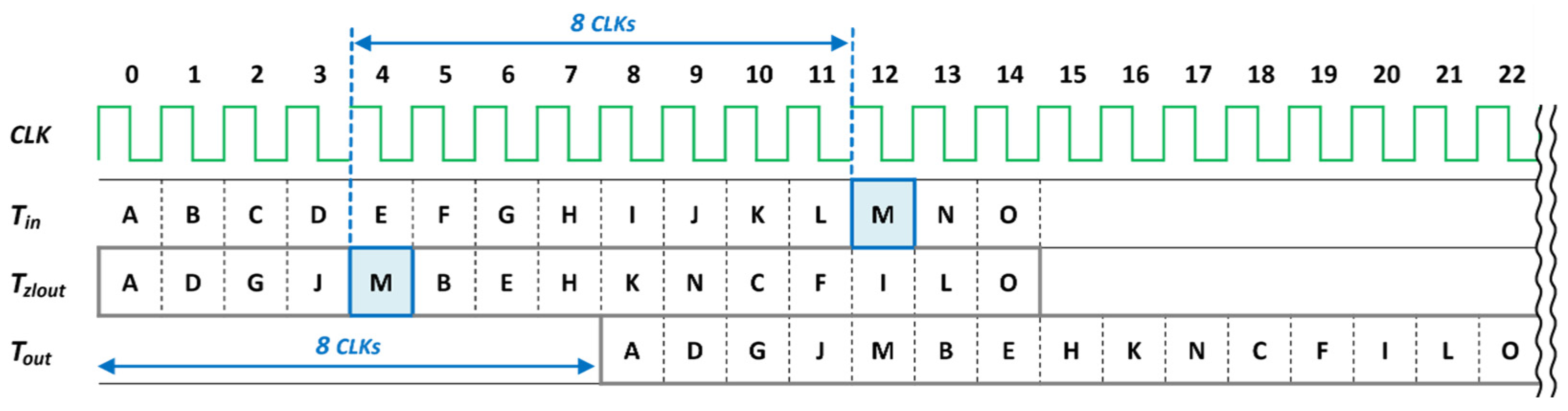
The complete lifetime information for all samples in the 5 × 3 block interleaver is summarized in Table 2, listing the input time T i n , T z l o u t , T d i f f , and T o u t for each data sample. This lifetime data forms the basis for calculating the number of concurrently active samples at each cycle [38,39]. Additionally, Figure 6 illustrates the timing relationship among T i n , T z l o u t , and T o u t for the 5 × 3 block interleaver. In this configuration, six of the fifteen samples exhibit negative T d i f f values, indicating violations of causality. Sample M presents the most severe violation, with T d i f f = 8, determining the global latency offset. By shifting all zero-latency output times by 8 clock cycles, the adjusted timing chart ensures causal validity for all outputs, defining the earliest feasible implementation schedule [43].
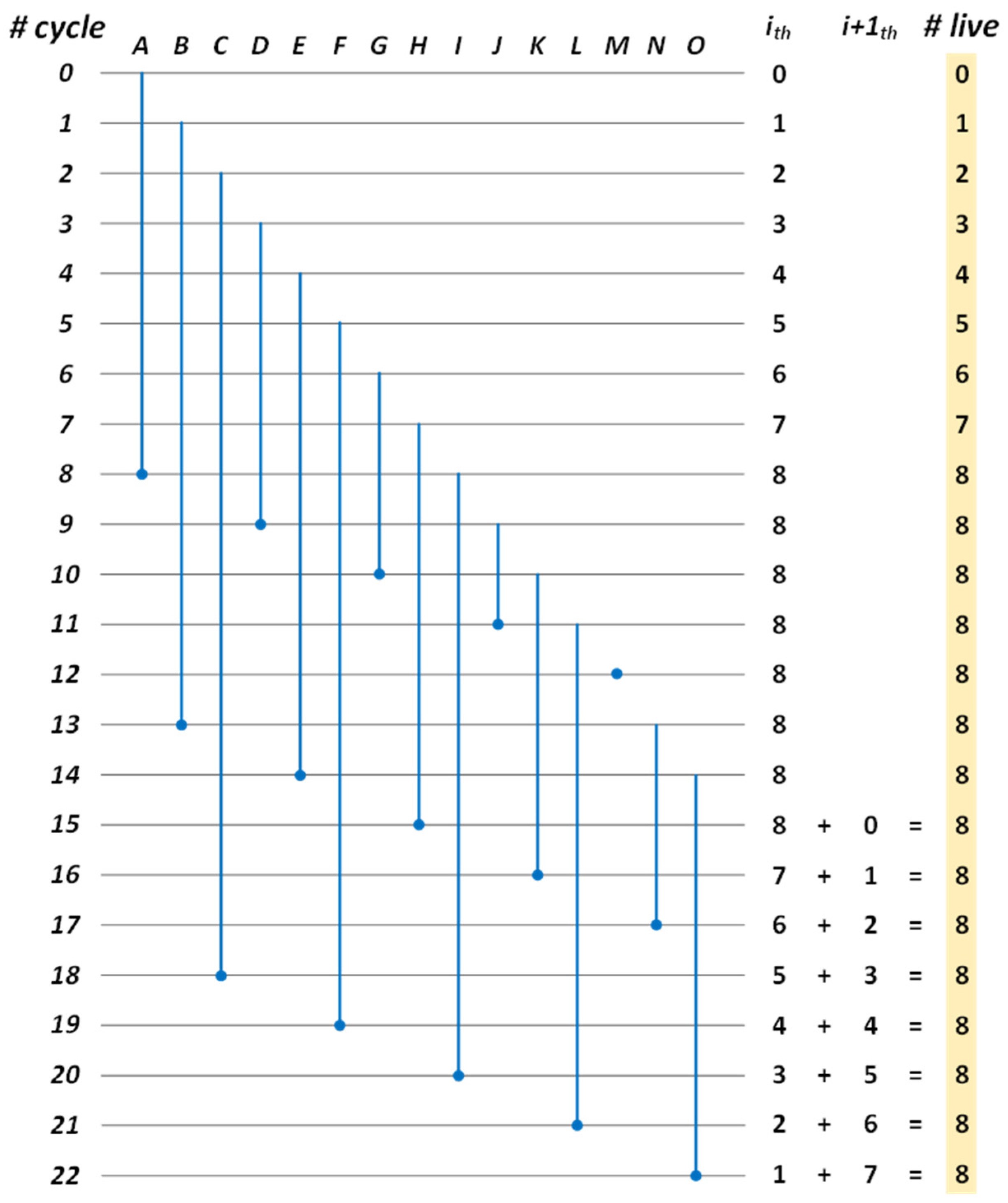
Based on the lifetime data in Table 2, a Lifetime Chart illustrating register activity over time can be constructed, as shown in Figure 7. This chart clearly indicates the required number of registers at each clock cycle by showing each data sample’s active period from T i n to T o u t [44]. The horizontal axis represents clock cycles, and each bar corresponds to the active period of an individual data sample. The number of concurrently active samples at a specific clock cycle directly indicates the number of registers required at that moment. For instance, at clock cycle 10, eight samples (B, C, E, F, G, H, I, J) are concurrently active, indicating that at least eight registers are necessary at this point. Thus, the maximum number of concurrently active samples during the entire interleaving process defines the minimum number of registers required for implementation.
This value represents the worst-case scenario for register usage from natural-order input to interleaved-order output. While this analysis provides a lower bound for a single interleaving cycle, practical systems must consider continuous data streaming. Specifically, sequential block interleavers require analyzing overlapping lifetimes across consecutive interleaving cycles. In such continuous-operation scenarios, the total number of required registers depends on the combined number of samples remaining active from the end of the i -th interleaving period and new samples entering at the start of the ( i + 1 )-th period. According to Figure 7, even when considering continuous data flow into the subsequent interleaving period, the maximum number of concurrently active samples remains eight. This result indicates that only eight registers are necessary to support continuous operation of the 5 × 3 block interleaver without any additional hardware or data collision.

3.2. Forward–Backward Register Allocation

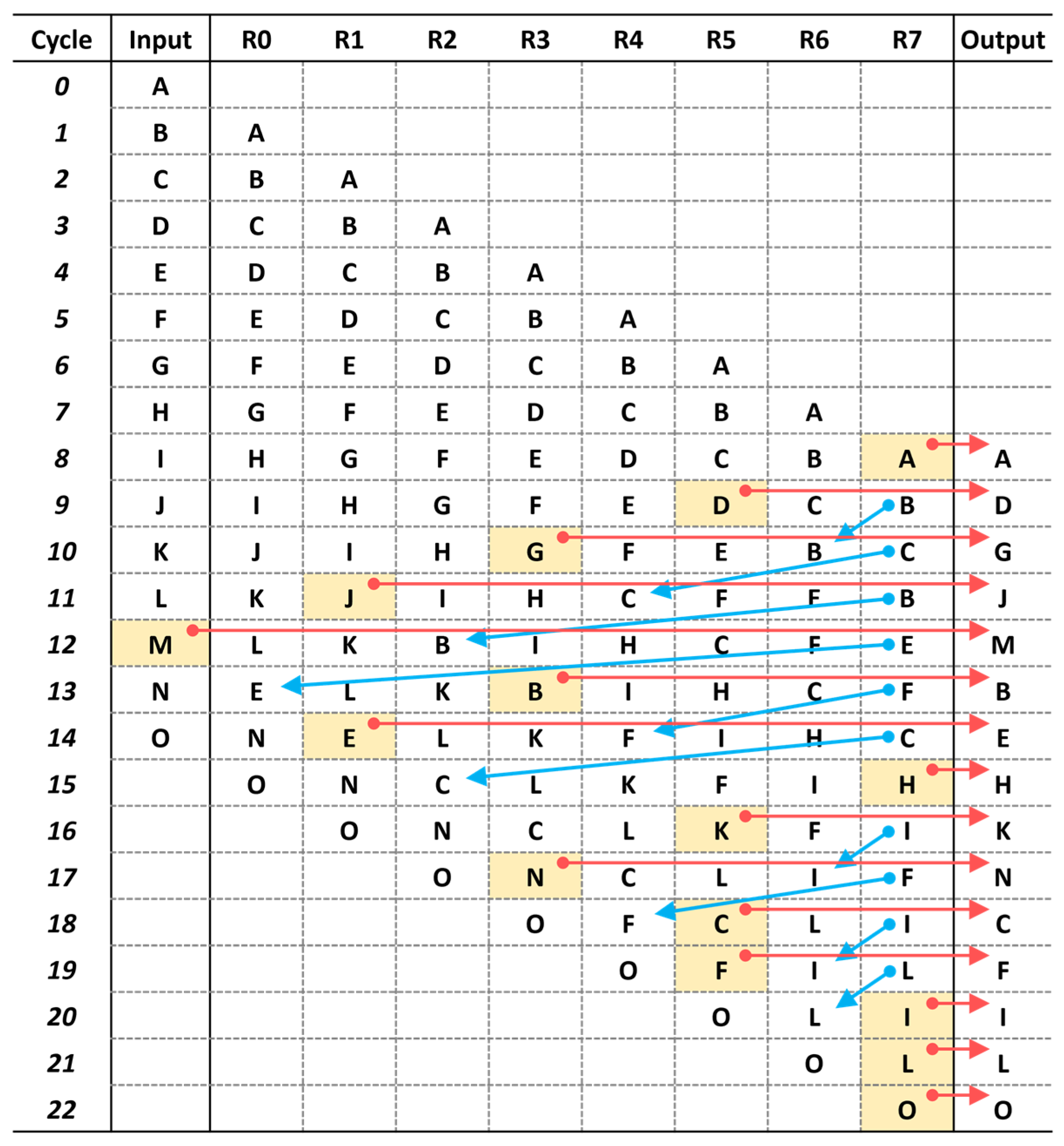
As shown in Figure 4, the conventional 5 × 3 block interleaver typically requires 30 registers for continuous data processing. However, the lifetime analysis, as shown in Figure 7, indicates that only eight registers are necessary. Thus, an efficient register allocation strategy is essential as the next step toward hardware implementation to effectively utilize this minimal set. In the proposed interleaver architecture, a Forward–Backward Register Allocation based on data lifetime information is utilized. This method assigns incoming data samples first in a forward manner and then, for samples with remaining lifetimes, reallocates registers in a backward manner [45]. To clarify this approach, consider the minimal set of eight registers labeled R0 through R7, each assumed to have a shift-register structure. Initially, incoming data samples are sequentially assigned to registers starting from R0 and shifted forward each clock cycle using forward allocation. Data samples with lifetimes of eight cycles or fewer expire naturally before reaching the final register R7, thus requiring only forward allocation. However, samples whose lifetimes exceed eight cycles remain active upon reaching the final register R7, necessitating backward allocation. In these cases, backward allocation reassigns the samples to available registers previously occupied by samples whose lifetimes have expired. As lifetime analysis guarantees a maximum of eight concurrently active samples, availability of registers for backward reallocation is always ensured [46].
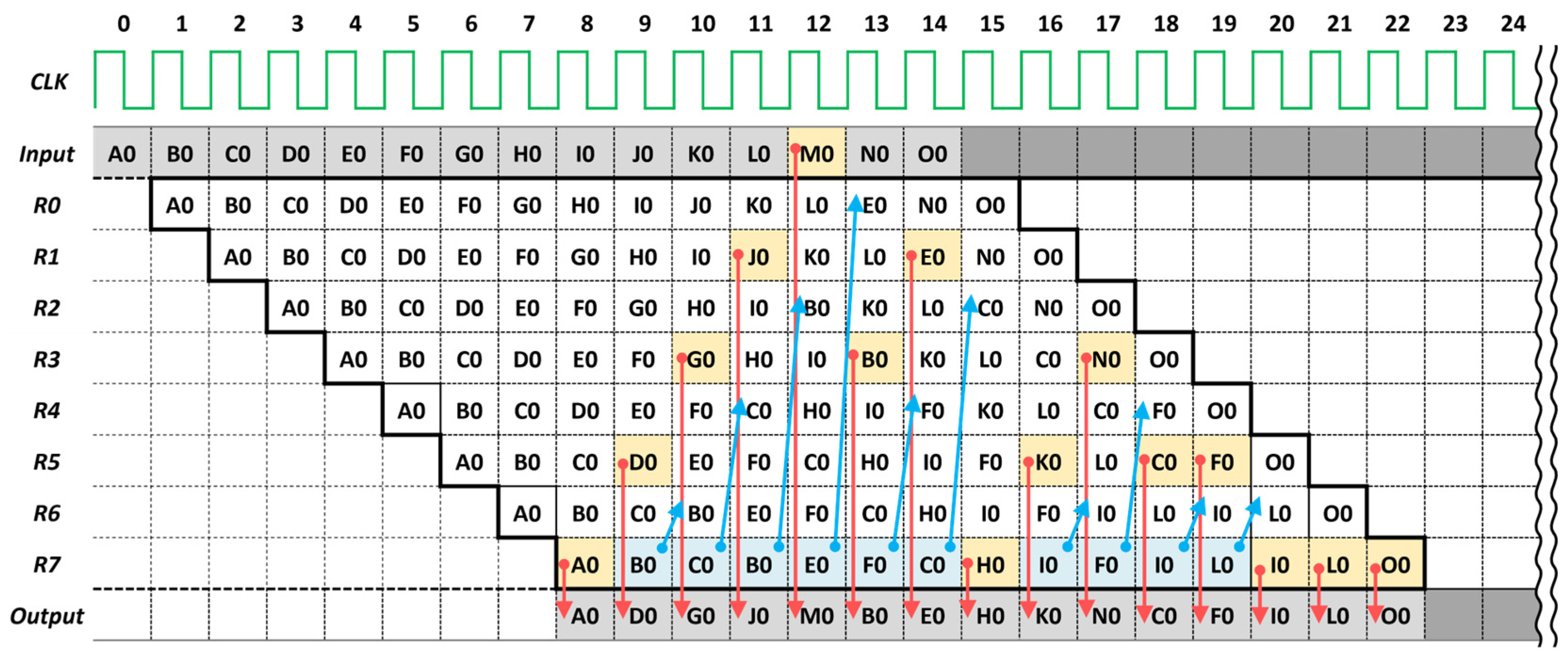
Figure 8 presents the Register Allocation Table for the optimized 5 × 3 block inter leaver using the Forward–Backward approach. The horizontal axis indicates the eight registers (R0 to R7) determined by lifetime analysis, while the vertical axis represents clock cycles. Data samples A through O enter sequentially in natural order from cycle 0 to cycle. Furthermore, the proposed optimized allocation approach ensures efficient register utilization both within a single interleaving cycle and across consecutive cycles under continuous data flow conditions. Unlike the conventional structure that requires double buffering to prevent data collisions, the proposed register allocation shown in Figure 8 enables continuous and collision-free input/output interleaving with only eight registers.

3.3. Detailed Interleaver Hardware Architecture

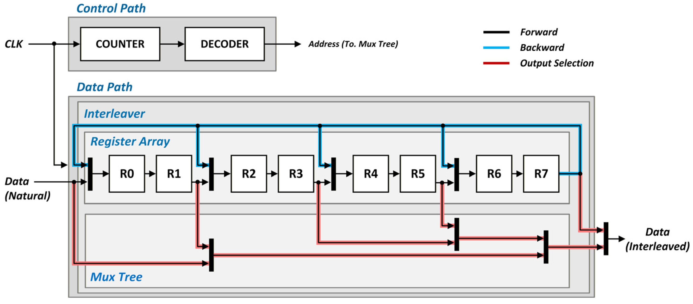
Based on the previously described register minimization and efficient allocation methods, this section details the proposed hardware architecture for the 5 × 3 block interleaver. Figure 9 illustrates the optimized hardware implementation, clearly highlighting the minimal number of registers and MUXs required. Specifically, the data paths are color-coded for clarity: forward reallocation in black, backward reallocation in blue, and output selection in red. The proposed architecture consists of eight registers, eight MUXs, and associated control circuits. The eight registers, labeled R0 through R7 as determined by Lifetime Analysis, are arranged in a shift-register configuration. Original data enter sequentially into register R0 and shift forward through subsequent registers with each clock cycle.
The conventional interleaver shown in Figure 4 requires double buffering and utilizes 30 registers to ensure continuous data processing. However, the proposed architecture efficiently achieves the same interleaving operation using only eight registers. Specifically, Forward Allocation is applied to data samples with lifetimes of eight cycles or fewer, as these samples naturally expire before reaching the final register R7. Conversely, Backward Allocation is employed for samples with lifetimes exceeding eight cycles, as these samples remain active upon reaching R7. These active samples are reassigned backward into previously freed registers, maximizing register reuse.
Additionally, the proposed architecture significantly reduces MUX requirements. Specifically, four MUXs are strategically placed between registers to enable backward data reallocation, guided by the Register Allocation Table shown in Figure 8. Another four MUXs are employed at the output stage to select the final interleaved outputs. Unlike the conventional structure, which requires N − 1 MUXs per register array, yielding a total of 29 MUXs, the proposed design restricts output selection specifically to the input, R1, R3, R5, and R7, thereby reducing the MUX count to eight. Lastly, the control logic systematically manages data movement and register selection, ensuring continuous and collision-free operation aligned with the proposed allocation strategy. In particular, the output MUX logic is derived from the Register Allocation Table in Figure 8, where the output selection at each clock cycle is determined by the register index in which the corresponding data sample was stored at the end of its lifetime. The highlighted region in Figure 8 represents the final output sequence obtained by rearranging data samples A ~ O according to the defined interleaving rule. In the 5 × 3 example, the interleaved data are restricted to be output from one of the following locations: the input, R1, R3, R5, and R7. Accordingly, the output stage in Figure 9 constructs the final interleaved sequence by hierarchically selecting the stored values from these registers using a cascade of 2-to-1 MUXs.
The control path, as shown in Figure 9, consists of a counter and a decoder, where the counter generates a cycle index indicating the current position within a block. The decoder takes this index as an input and generates the SEL signals for each MUX according to the predefined selection rule. This coordinated control enables deterministic register-to-register data reallocation and output selection at every clock cycle, thereby supporting continuous data streaming without register collisions.
Furthermore, Figure 10 presents the timing diagram of the proposed block interleaver, clearly demonstrating its operational advantage over the conventional structure shown in Figure 5. While the conventional interleaver requires numerous registers, many of which remain idle during operation, the proposed architecture achieves equivalent interleaving functionality with only eight registers and fully eliminates idle states. The timing diagram confirms complete register utilization, highlighting the improved efficiency of the proposed method. Lastly, the conventional double buffering approach introduces latency equal to the data length N. For example, when N = 15, outputs are produced 15 clock cycles after inputs. In contrast, the proposed architecture employs a global latency offset derived from Lifetime Analysis, enabling outputs to begin earlier specifically after only eight clock cycles. As a result, the proposed interleaver architecture ensures continuous data streaming with significantly reduced latency. Compared to the conventional double buffering structure, the earlier output start directly reduces the baseband processing latency of the interleaver stage. Consequently, the proposed design can also contribute to lowering the overall end-to-end latency in practical GNSS processing pipelines. As a result, this optimized hardware architecture significantly reduces the required number of registers and MUXs, leading to decreased hardware complexity, power consumption, and chip area. Simultaneously, it enhances latency performance, making it more suitable for efficient GNSS signal processing applications.

4. Experimental Results

To evaluate the effectiveness of the proposed interleaver architecture, several interleavers employed in modern GNSS signals listed in Table 1 were implemented. The performance of the proposed architecture was compared against the conventional architectures across seven interleaving configurations corresponding to the following signals: GPS L1C; BDS B1C, B1I, B2I, and B3I; Galileo E1B, E5a, E5b, and E6B; QZSS L1C; and NavIC L1 SPS, L5 SPS, and S SPS. Note that certain signals share identical interleaving schemes. Quantitative comparisons of hardware resource utilization between conventional and proposed architectures were first analyzed. Figure 11 clearly compares the required number of registers and MUXs, highlighting significant reductions achieved by the proposed architecture. Conventional architectures, depicted in Figure 4, typically require double buffering and extensive multiplexing to maintain continuous data outputs, resulting in increased hardware complexity. Specifically, hardware complexity scales directly with interleaving size N, posing substantial challenges for larger interleavers. In contrast, the proposed architecture shown in Figure 9 utilizes Lifetime Analysis and Forward–Backward Register Allocation to significantly minimize register usage and optimize resource utilization. Quantitative results indicated average reductions of approximately 45.80% in register count and 58.51% in MUX count, demonstrating that the proposed architecture nearly halves hardware complexity without degrading interleaving performance.
To further validate these improvements practically, synthesis experiments were performed using a standard 28 nm CMOS process. All interleaver configurations were implemented in Verilog Hardware Description Language (HDL) and synthesized using Synopsys Design Compiler at an operating frequency of 500 MHz. Table 3 summarizes key implementation results, including chip area, power consumption, and latency for both conventional and proposed architectures across all evaluated GNSS interleavers. As interleavers primarily consist of registers and MUXs, reductions in these elements directly correlate with improvements in chip area and power consumption. According to the synthesis results, the proposed architecture achieved substantial average improvements of approximately 38.82% in chip area and 52.01% in power consumption, respectively. Although the improvement ratio tends to decrease as the interleaver size increases and the control path occupies approximately 40% of the total area, the proposed architecture consistently maintains superior performance compared to the conventional method. These improvements align closely with the quantitative hardware resource reductions illustrated previously in Figure 11, confirming that efficiency improvements are primarily driven by decreased register and MUX usage. The proposed architecture also improved latency by approximately 25.05% compared to conventional designs. This latency reduction results from completely eliminating double buffering and leveraging the global latency offset calculated through Lifetime Analysis, allowing outputs to begin at the earliest feasible clock cycle.
In summary, the experimental results consistently confirm performance improvements across all existing GNSS interleaver configurations. The proposed architecture significantly reduces hardware complexity, chip area, power consumption, and latency without sacrificing interleaving performance. These advantages underscore its practical suitability for efficient implementation in current and next-generation GNSS applications.

5. Conclusions

This paper proposed an optimized hardware architecture for interleaving in modern GNSS using Lifetime Analysis and Forward–Backward Register Allocation techniques. Conventional GNSS interleavers typically require significant hardware resources, including numerous registers, and MUXs, leading to increased chip area, power consumption, and latency. To address these issues, Lifetime Analysis was employed to precisely determine the minimum register count, significantly reducing hardware redundancy. Additionally, Forward–Backward Register Allocation was utilized to maximize the efficiency of register utilization. This method systematically allocates data samples based on their lifetime information, ensuring that each register is optimally employed throughout the entire interleaving process. The synthesis results demonstrated substantial improvements compared to conventional architectures, with average reductions of approximately 38.82% in chip area and 52.01% in power consumption. Additionally, latency performance improved by approximately 25.05% by eliminating the double buffering structure and implementing a global latency offset calculated through Lifetime Analysis, allowing outputs to begin significantly earlier. These experimental results confirm that the proposed interleaver architecture effectively maintains robust interleaving performance while minimizing hardware complexity and resource usage. The reduced complexity leads directly to lower power consumption and a smaller chip footprint, making the proposed approach highly suitable for resource-constrained GNSS receivers and satellite payloads. The architecture also ensures continuous, collision-free data streaming with improved latency performance. Therefore, the proposed optimized hardware interleaver architecture presents a significant advancement in addressing practical GNSS implementation challenges, offering substantial benefits for current and future navigation systems.

Author Contributions

H.Y. conceived the main idea, designed the methodology, and supervised; J.H. designed the HDL, conducted experiments, analyzed data, and wrote the manuscript; K.K., D.K., and J.S. assisted with writing and editing; S.-Y.S., Y.-H.K. and J.-U.P. assisted with experiments and analysis. All authors have read and agreed to the published version of the manuscript.

Funding

This research was supported by the Korea AeroSpace Administration (KASA), Government of the Republic of Korea (Grant No. RS-2022-00165808).

Data Availability Statement

The data analyzed during the current study are not publicly available due to the management regulations of relevant organizations but are partly available from the corresponding author on reasonable request.

Conflicts of Interest

Authors Yo-Han Ko and Jong-Uk Park were employed by the company LIG Nex1. The remaining authors declare that the research was conducted in the absence of any commercial or financial relationships that could be construed as a potential conflict of interest.

References

  1. Kaplan, E.D.; Hegarty, C. Understanding GPS/GNSS: Principles and Applications; Artech House: Boston, MA, USA, 2017. [Google Scholar]
  2. Borre, K.; Fernández-Hernández, I.; López-Salcedo, J.A.; Bhuiyan, M.Z.H. GNSS Software Receivers; Cambridge University Press: Cambridge, UK, 2022. [Google Scholar]
  3. GPS Directorate. Navstar GPS Space Segment/Navigation User Interfaces (IS GPS-200), Revision N; Technical Report; U.S. Department of Defense: Washington, DC, USA, 2022. Available online: https://archive.gps.gov/technical/icwg/ (accessed on 25 August 2025).
  4. Russian Space Systems. GLONASS Interface Control Document, Edition 5.1; Technical Report; Russian Institute of Space Device Engineering: Moscow, Russia, 2008; Available online: https://www.glonass-iac.ru/en/ (accessed on 25 August 2025).
  5. Yao, Z.; Lu, M. Next-Generation GNSS Signal Design; Springer: Singapore, 2021. [Google Scholar]
  6. Sánchez-Ortiz, C.R.; Parra-Michel, R.; Guzmán-Rentería, M.E. Design and implementation of a multi-standard interleaver for 802.11 a, 802.11 n, 802.16 e & dvb standards. In Proceedings of the 2008 International Conference on Reconfigurable Computing and FPGAs, Cancun, Mexico, 3–5 December 2008; IEEE: New York, NY, USA; pp. 379–384. [Google Scholar]
  7. Sklar, B. Digital Communications: Fundamentals and Applications; Pearson: Boston, MA, USA, 2021. [Google Scholar]
  8. GPS Directorate. Navstar GPS Space Segment/User Interfaces (IS-GPS-705), Revision J; Technical Report; U.S. Department of Defense: Washington, DC, USA, 2022. Available online: https://archive.gps.gov/technical/icwg/ (accessed on 25 August 2025).
  9. GPS Directorate. Navstar GPS Space Segment/User Interfaces (IS-GPS-800), Revision J; Technical Report; U.S. Department of Defense: Washington, DC, USA, 2022. Available online: https://archive.gps.gov/technical/icwg/ (accessed on 25 August 2025).
  10. International GNSS Service (IGS) Multi-GNSS Experiment (MGEX): MGEX Constellations–GPS. Available online: https://igs.org/mgex/constellations/#gps (accessed on 25 August 2025).
  11. European Union Agency for the Space Programme (EUSPA). Galileo Open Service Signal-in-Space Interface Control Document, Issue 2.0; Technical Report; European Union: Prague, Czech Republic, 2016; Available online: https://www.gsc-europa.eu/ (accessed on 25 August 2025).
  12. European Union Agency for the Space Programme (EUSPA). Galileo High Accuracy Service Signal-in-Space Interface Control Document; Technical Report; European Union: Prague, Czech Republic, 2021; Available online: https://www.gsc-europa.eu/ (accessed on 25 August 2025).
  13. European GNSS Agency (GSA). Galileo Commercial Service (CS) Signal-in Space Interface Control Document, Issue 1.0; Technical Report; European Union: Prague, Czech Republic, 2019; Available online: https://www.gsc-europa.eu/ (accessed on 25 August 2025).
  14. International GNSS Service (IGS) Multi-GNSS Experiment (MGEX): MGEX Constellations–Galileo. Available online: https://igs.org/mgex/constellations/#galileo (accessed on 25 August 2025).
  15. International GNSS Service (IGS) Multi-GNSS Experiment (MGEX): MGEX Constellations–GLONASS. Available online: https://igs.org/mgex/constellations/#glonass (accessed on 25 August 2025).
  16. China Satellite Navigation Office. BeiDou Navigation Satellite System Signal in Space Interface Control Document, Open Service Signal B1I; Technical Report; CSNO: Beijing, China, 2017. Available online: http://en.beidou.gov.cn/SYSTEMS/ICD/ (accessed on 25 August 2025).
  17. China Satellite Navigation Office. BeiDou Navigation Satellite System Signal in Space Interface Control Document, Open Service Signals B1C and B2a; Technical Report; CSNO: Beijing, China, 2017. Available online: http://en.beidou.gov.cn/SYSTEMS/ICD/ (accessed on 25 August 2025).
  18. China Satellite Navigation Office. BeiDou Navigation Satellite System Signal in Space Interface Control Document, Open Service Signal B3I; Technical Report; CSNO: Beijing, China, 2018. Available online: http://en.beidou.gov.cn/SYSTEMS/ICD/ (accessed on 25 August 2025).
  19. International GNSS Service (IGS) Multi-GNSS Experiment (MGEX): MGEX Constellations–BeiDou. Available online: https://igs.org/mgex/constellations/#beidou (accessed on 25 August 2025).
  20. Cabinet Office, Government of Japan. Quasi-Zenith Satellite System Interface Specification (IS-QZSS); Technical Report; Cabinet Office, Japan: Tokyo, Japan, 2018; Available online: https://qzss.go.jp/en/technical/ (accessed on 25 August 2025).
  21. International GNSS Service (IGS) Multi-GNSS Experiment (MGEX): MGEX Constellations–QZSS. Available online: https://igs.org/mgex/constellations/#qzss (accessed on 25 August 2025).
  22. Indian Space Research Organisation (ISRO). Indian Regional Navigation Satellite System (IRNSS) Signal in Space Interface Control Document for Standard Positioning Service; Technical Report; ISRO: Bengaluru, India, 2017. Available online: https://www.isro.gov.in/ (accessed on 25 August 2025).
  23. International GNSS Service (IGS) Multi-GNSS Experiment (MGEX): MGEX Constellations–NavIC. Available online: https://igs.org/mgex/constellations/#navic (accessed on 25 August 2025).
  24. Tell, E.; Liu, D. A hardware architecture for a multimode block interleaver. In Proceedings of the International Conference on Circuits and Systems for Communications (ICCSC), Moscow, Russia, 27–29 June 2004. [Google Scholar]
  25. Chavet, C.; Sani, A.H.; Coussy, P. Hardware design of parallel interleaver architectures: A survey. In Advanced Hardware Design for Error Correcting Codes; Springer: Cham, Switzerland, 2014; pp. 177–192. [Google Scholar]
  26. Zhang, Z.-d.; Wu, B.; Zhou, Y.-m.; Zhang, X. Low-complexity hardware inter leaver/deinterleaver for ieee 802.11 a/g/n wlan. VLSI Des. 2012, 2012, 948957. [Google Scholar] [CrossRef]
  27. Xiong, X.; Dai, Y.; Hu, Z.; Huo, K.; Bai, Y.; Li, H.; Liu, D. Hardware sharing for channel interleavers in 5g nr standard. Secur. Commun. Netw. 2021, 2021, 8872140. [Google Scholar] [CrossRef]
  28. Wang, G.; Shen, H.; Sun, Y.; Cavallaro, J.R.; Vosoughi, A.; Guo, Y. Parallel interleaver design for a high throughput hspa+/lte multi-standard turbo decoder. IEEE Trans. Circuits Syst. I Regul. Pap. 2014, 61, 1376–1389. [Google Scholar] [CrossRef]
  29. Shivaramaiah, N.C.; Dempster, A.G. Baseband hardware designs in modernised gnss receivers. In Global Navigation Satellite Systems: Signal, Theory and Applications; IntechOpen: London, UK, 2012. [Google Scholar]
  30. Grenier, A.; Lohan, E.S.; Ometov, A.; Nurmi, J. A survey on low-power gnss. IEEE Commun. Surv. Tutor. 2023, 25, 1482–1509. [Google Scholar] [CrossRef]
  31. Egea-Roca, D.; Arizabaleta-Diez, M.; Pany, T.; Antreich, F.; Lopez-Salcedo, J.A.; Paonni, M.; Seco-Granados, G. Gnss user technology: State-of-the-art and future trends. IEEE Access 2022, 10, 39939–39968. [Google Scholar] [CrossRef]
  32. Park, J.U.; Heo, M.B. Korea pnt update. In Proceedings of the 59th Meeting of the Civil GPS Service Interface Committee, Miami, FL, USA, 16–17 September 2019; pp. 16–17. [Google Scholar]
  33. Hofmann-Wellenhof, B.; Lichtenegger, H.; Wasle, E. GNSS—Global Navigation Satellite Systems: GPS, GLONASS, Galileo, and More; Springer: Berlin/Heidelberg, Germany, 2008. [Google Scholar]
  34. Huffman, W.C.; Pless, V. Fundamentals of Error-Correcting Codes; Cambridge University Press: Cambridge, UK, 2010. [Google Scholar]
  35. Anghileri, M.; Paonni, M.; Fontanella, D.; Eissfeller, B. Assessing gnss data message performance a new approach. Inside GNSS 2013, 2, 60–70. [Google Scholar]
  36. Shetty, N.R.; Prasad, N.H.; Nalini, N. Emerging Research in Computing, Information, Communication and Applications; Springer: Singapore, 2022. [Google Scholar]
  37. Huang, K.-Y.; Juang, J.-C.; Tsai, Y.-F.; Lin, C.-T. Efficient fpga implementation of a dual-frequency gnss receiver with robust inter-frequency aiding. Sensors 2021, 21, 4634. [Google Scholar] [CrossRef] [PubMed]
  38. Parhi, K.K. Systematic synthesis of dsp data format converters using life-time analysis and forward-backward register allocation. IEEE Trans. Circuits Syst. II Analog. Digit. Signal Process. 2002, 39, 423–440. [Google Scholar] [CrossRef]
  39. Parhi, K.K. VLSI Digital Signal Processing Systems: Design and Implementation; John Wiley & Sons: Hoboken, NJ, USA, 2007. [Google Scholar]
  40. Ayinala, M.; Brown, M.; Parhi, K.K. Pipelined parallel fft architectures via folding transformation. IEEE Trans. Very Large Scale Integr. (VLSI) Syst. 2011, 20, 1068–1081. [Google Scholar] [CrossRef]
  41. Parhi, K.K. Calculation of minimum number of registers in arbitrary life time chart. IEEE Trans. Circuits Syst. II Analog. Digit. Signal Process. 2002, 41, 434–436. [Google Scholar] [CrossRef]
  42. Parhi, K.K.; Nishitani, T. Vlsi architectures for discrete wavelet transforms. IEEE Trans. Very Large Scale Integr. (VLSI) Syst. 1993, 1, 191–202. [Google Scholar] [CrossRef]
  43. Parhi, K.K. Video data format converters using minimum number of registers. IEEE Trans. Circuits Syst. Video Technol. 2002, 2, 255–267. [Google Scholar] [CrossRef]
  44. Majumdar, M.; Parhi, K.K. Design of data format converters using two dimensional register allocation. IEEE Trans. Circuits Syst. II: Analog. Digit. Signal Process. 2002, 45, 504–508. [Google Scholar] [CrossRef]
  45. Denk, T.C.; Parhi, K.K. Synthesis of folded pipelined architectures for multirate dsp algorithms. IEEE Trans. Very Large Scale Integr. (VLSI) Syst. 2002, 6, 595–607. [Google Scholar] [CrossRef]
  46. Parhi, K.K.; Lee, J.-S. Register allocation for design of data format converters. In Proceedings of the [Proceedings] ICASSP 91: 1991 International Conference on Acoustics, Speech, and Signal Processing, Toronto, ON, Canada, 14–17 April 1991; IEEE: New York, NY, USA; pp. 1133–1136. [Google Scholar]
Figure 1. Block diagram of GNSS signal transmission and reception illustrating random and burst error sources.
Electronics 15 00526 g001
Figure 2. Operation of a 5 × 3 block interleaver: (a) without interleaving; (b) with interleaving.
Electronics 15 00526 g002
Figure 3. Effect of interleaving on burst error correction in FEC systems: (a) without interleaving; (b) with interleaving.
Electronics 15 00526 g003
Figure 4. Conventional 5 × 3 sequential block interleaver architecture.
Electronics 15 00526 g004
Figure 5. Conventional 5 × 3 block interleaver timing diagram.
Electronics 15 00526 g005
Figure 6. Operational timing sequence of 5 × 3 block interleaver.
Electronics 15 00526 g006
Figure 7. Lifetime chart for 5 × 3 sequential block interleaver.
Electronics 15 00526 g007
Figure 8. Register allocation table for 5 × 3 sequential block interleaver.
Electronics 15 00526 g008
Figure 9. Proposed 5 × 3 block interleaver architecture.
Electronics 15 00526 g009
Figure 10. Timing Diagram for the proposed 5 × 3 block interleaver architecture.
Electronics 15 00526 g010
Figure 11. Hardware resource comparison between the conventional and proposed interleaver architectures: (a) Register comparison; (b) MUX comparison.
Electronics 15 00526 g011
Table 1. Summary of GNSS/RNSS signals and interleaver usage.
ConstellationSignalTypeInterleaver SizeYear
GPSL1C/AGNSS 1978
L2CGNSS 2005
L5GNSS 2010
L1CGNSS38 × 462018
GLONASSL1OFGNSS 1982
L2OFGNSS 2003
L3OCGNSS 2003
L2OCGNSS 2011
L1OCGNSS 2017
GalileoE1BGNSS8 × 302011
E5aGNSS8 × 612011
E5bGNSS8 × 302011
E6BGNSS8 × 1232011
BDSB1IGNSS2 × 152007
B2IGNSS2 × 152007
B3IGNSS2 × 152007
B2aGNSS 2015
B2bGNSS 2015
B1CGNSS36 × 482015
QZSSL1C/ARNSS 2010
L2CRNSS 2010
L5RNSS 2010
L1CRNSS38 × 462010
L1C/BRNSS 2021
NavICL5 SPSRNSS8 × 732013
S SPSRNSS8 × 732013
L1 SPSRNSS38 × 462023
Note. Signal specifications are based on official ICDs, and broadcasting years are referenced from International GNSS Service (IGS) Multi-GNSS Experiment (MGEX) constellation service pages: GPS [3,8,9,10], Galileo [11,12,13,14], GLONASS [4,15], BDS [16,17,18,19], QZSS [20,21], and NavIC [22,23].
Table 2. Lifetime table for 5 × 3 sequential block interleaver.
Sample T i n T z l o u t T d i f f T o u t Life Period
A00080 8 (8)
B154131 13 (12)
C2108182 18 (16)
D31 2 *93 9 (6)
E462144 14 (10)
F5116195 19 (14)
G62 4 *106 10 (4)
H770157 15 (8)
I8124208 20 (12)
J93 6 *119 11 (2)
K108 2 *1610 16 (6)
L111322111 21 (10)
M124 8 **1212 12 (0)
N139 4 *1713 17 (4)
O141402214 22 (8)
Note. Values with T d i f f < 0 are marked with *; the minimum with **.
Table 3. Synthesis results for GNSS block interleavers (28 nm CMOS).
GPSBDSGalileoQZSSNavICAverage
L1CB1CB1IB2IB3IE1BE5aE5bE6BL1CL1 SPSL5 SPSS SPS
Size 38 × 46 36 × 48 2 × 15 2 × 15 2 × 15 8 × 30 8 × 61 8 × 30 8 × 123 38 × 46 38 × 46 8 × 73 8 × 73 16 × 48
Area ( 10 3 μ m 2 )
 Conv.14.5314.350.280.280.282.034.152.038.2214.5314.534.894.896.54
 Prop.10.5210.390.110.110.111.252.611.255.5010.5210.523.303.304.58
 Imp. (%)27.6027.6060.7160.7160.7138.4237.1138.4233.0927.6027.6032.5232.5238.82
Power (mW)
 Conv.7.917.820.160.160.161.122.241.124.467.917.912.672.673.56
 Prop.4.234.220.060.060.060.551.100.552.234.234.231.331.331.86
 Imp. (%)46.5246.0462.5062.5062.5050.8950.8950.8950.0046.5246.5250.1950.1952.01
Latency (#cycle)
 Conv.1748172830303024048824098417481748584584783.23
 Prop.166516451414142034205685416651665504504709.46
 Imp. (%)4.754.8053.3353.3353.3315.4213.9376.6713.214.754.7513.7013.7025.05
Abbreviations: Conv. = conventional; Prop. = proposed; Imp. = improvement, computed as (Conv. Prop.)/Conv. × 100%.
Disclaimer/Publisher’s Note: The statements, opinions and data contained in all publications are solely those of the individual author(s) and contributor(s) and not of MDPI and/or the editor(s). MDPI and/or the editor(s) disclaim responsibility for any injury to people or property resulting from any ideas, methods, instructions or products referred to in the content.