1. Introduction
Increasing data rates in optical and radio-over-fiber (RoF) networks place stringent demands on receiver front-end circuits [
1,
2]. Transimpedance amplifiers (TIAs) form the critical interface between current-domain photodiodes and subsequent voltage-mode processing, and must therefore provide high gain, low noise, and efficient use of area and power [
3,
4]. Contemporary TIA designs emphasize broadband operation and gain programmability to accommodate varying signal conditions, as demonstrated by regulated-cascode and multi-stage variable-gain architectures targeting multi-GHz bandwidths [
5]. Another key application for optical circuits is microwave-photonics, which involves the integration of photonic components into microwave architectures [
6,
7,
8]. In RoF small-cell receivers, however, purely wideband transimpedance responses are often suboptimal, since front-end selectivity is required to suppress out-of-band interference before subsequent amplification and mixing stages [
9]. This motivates integrating frequency-selective behavior directly at the transimpedance interface, particularly in architectures where receiver channelization is performed at, or close to, the photodiode interface [
10].
Transimpedance bandpass filters address this requirement by combining current-to-voltage conversion and band-pass filtering within a single transfer function. Active transimpedance band-pass formulations support a wide range of
Q values through biquadratic synthesis [
11], while MOS-C and MOS-only realizations offer compact, IC-compatible implementations where tunability is achieved through transconductance control and integrated capacitors [
12]. These prior formulations serve as useful benchmarks; however, many reported tunable band-pass TIA implementations exhibit limited orthogonality between tuning parameters. In particular, adjusting the center frequency often results in concurrent variations in transimpedance gain and bandwidth. In addition, several reported designs rely on relatively high power consumption, often in the range of 5–30 mW, which is undesirable for dense RoF small-cell deployments [
13]. These observations motivate a symbolic synthesis flow that captures the coupling between center frequency, gain, and
Q-factor while supporting power-efficient, post-layout verified designs. This work therefore investigates the symbolic synthesis and optimization of a tunable transimpedance band-pass filter for 5G RoF small-cell front-end applications.
The demand for area-efficient, low-power, and tunable filter topologies has driven the adoption of symbolic exploration as a rigorous methodology for circuit synthesis. Elamien et al. utilized this approach to systematically investigate minimal-transistor architectures, leading to the development of novel first-order [
14] and second-order all-pass filters [
15,
16], some of which were successfully fabricated and validated in 65 nm CMOS. Furthermore, symbolic techniques have proven effective in synthesizing more complex structures such as quadrature-phase oscillators [
17]. A key advantage of symbolic exploration is that it yields closed-form expressions that enable rapid topology pruning, parametric sensitivity analysis, and explainable trade-off reasoning prior to computationally expensive simulation campaigns.
Recent advancements in Electronic Design Automation (EDA) have increasingly combined machine learning (ML) with circuit abstractions to accelerate early-stage design exploration [
18]. For example, frameworks based on Graph Neural Networks and Variational Autoencoders can learn structural priors and generate candidate topologies that are subsequently mapped to transistor-level implementations [
19]. However, SPICE simulations remain computationally expensive, and scalable exploration therefore benefits from symbolic analysis during the earliest stages of topology selection and sizing. While symbolic solvers have been utilized in research, they are frequently constrained by proprietary licenses or limited to educational contexts [
20]. The lack of interoperable open-source tooling often forces researchers to implement custom data structures, expression handling, and validation logic, reducing code reusability and complicating integration with modern optimization and ML toolchains. Moreover, quantitative comparison between symbolic expressions remains challenging.
To address these limitations,
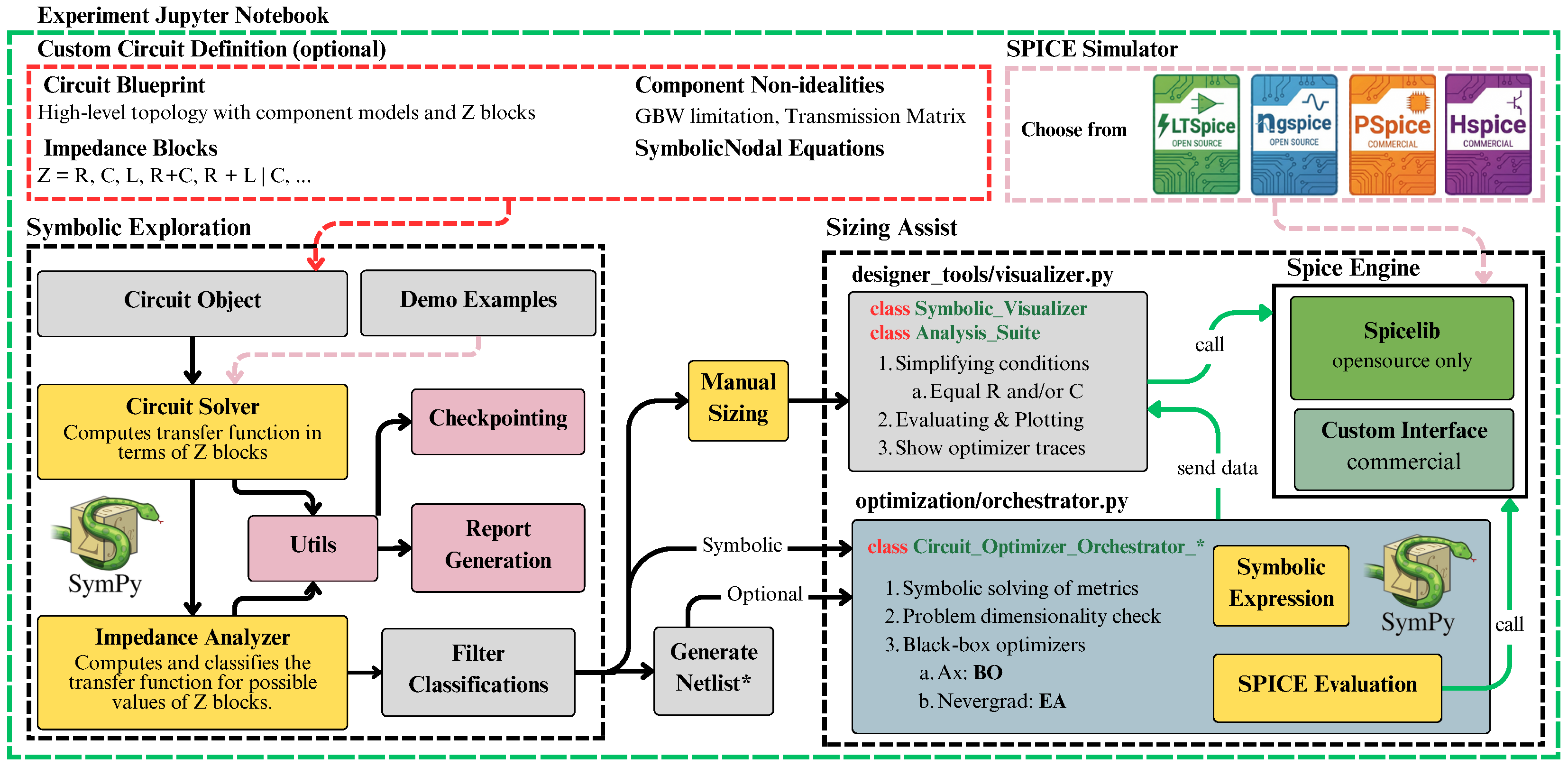
Figure 1 summarizes the workflow of SymXplorer, an open-source framework for symbolic topology exploration and circuit sizing with SPICE-consistent validation. The main contributions of this work are threefold: (i) a modular symbolic exploration engine for systematically enumerating and analyzing candidate topologies, (ii) an integrated sizing toolbox that supports optimization-driven tuning of design variables, and (iii) a unified characterization flow that aligns symbolic transfer functions with transistor-level and post-layout SPICE verification. SymXplorer is designed to be simulator-agnostic and optimization-agnostic, enabling integration with standard SPICE engines and a wide range of optimization strategies [
21,
22] while remaining usable out of the box. This modularity also positions SymXplorer as a practical backend for emerging agent-based EDA workflows, where symbolic representations provide an efficient interface between reasoning agents, learning-based optimizers, and transistor-level verification.
The remainder of this paper is organized as follows:
Section 2 details the algorithmic architecture of SymXplorer, focusing on the symbolic exploration logic and the integrated circuit sizing toolbox.
Section 3 presents a case study of a tunable band-pass TIA implemented in 65 nm CMOS, including post-layout results.
Section 4 explains the effects of physical non-idealities through symbolic analysis, discusses methodologies for synthesizing transistor-level implementations from symbolic results, and outlines a roadmap for integrating agentic AI into autonomous EDA workflows. Finally, the paper concludes with a summary of key findings and future research directions.
4. Discussion
This section analyzes the simulation results and the impact of component non-idealities on circuit performance. It also explores future research directions for integrating these findings into automated EDA workflows to improve design efficiency.
4.1. Analysis: Modeling the Effects of Non-Idealities
The
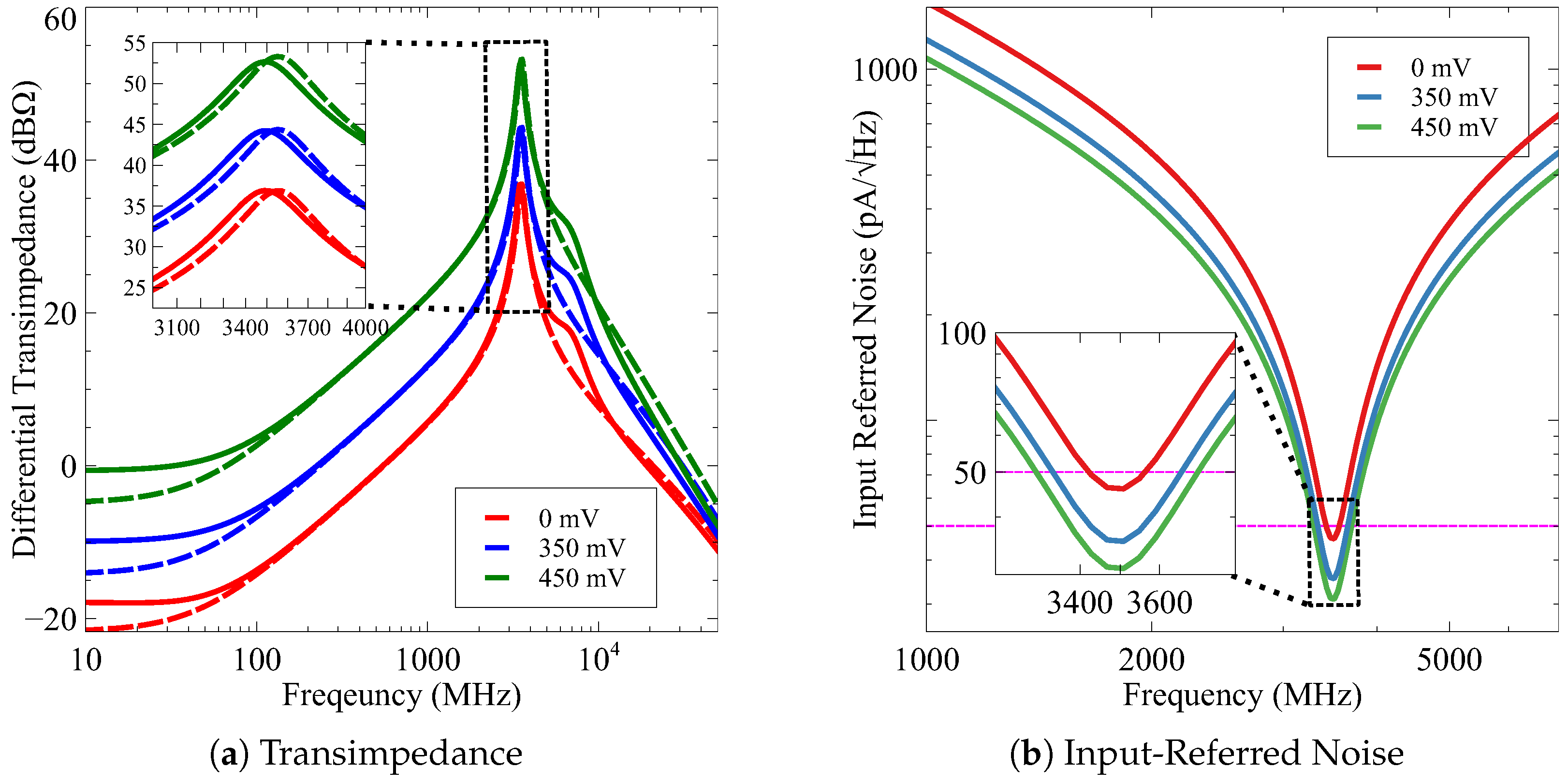
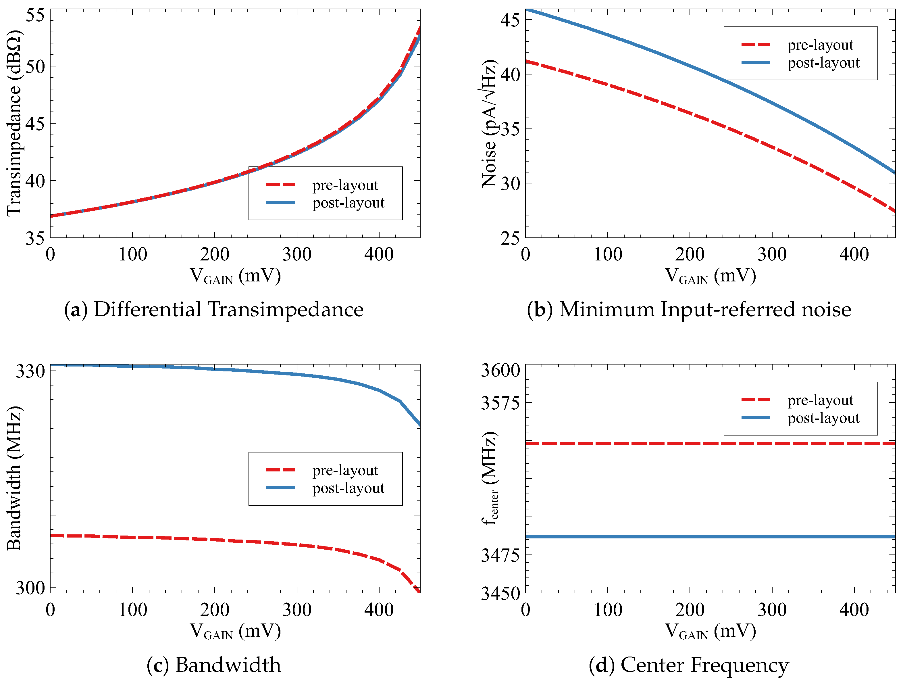
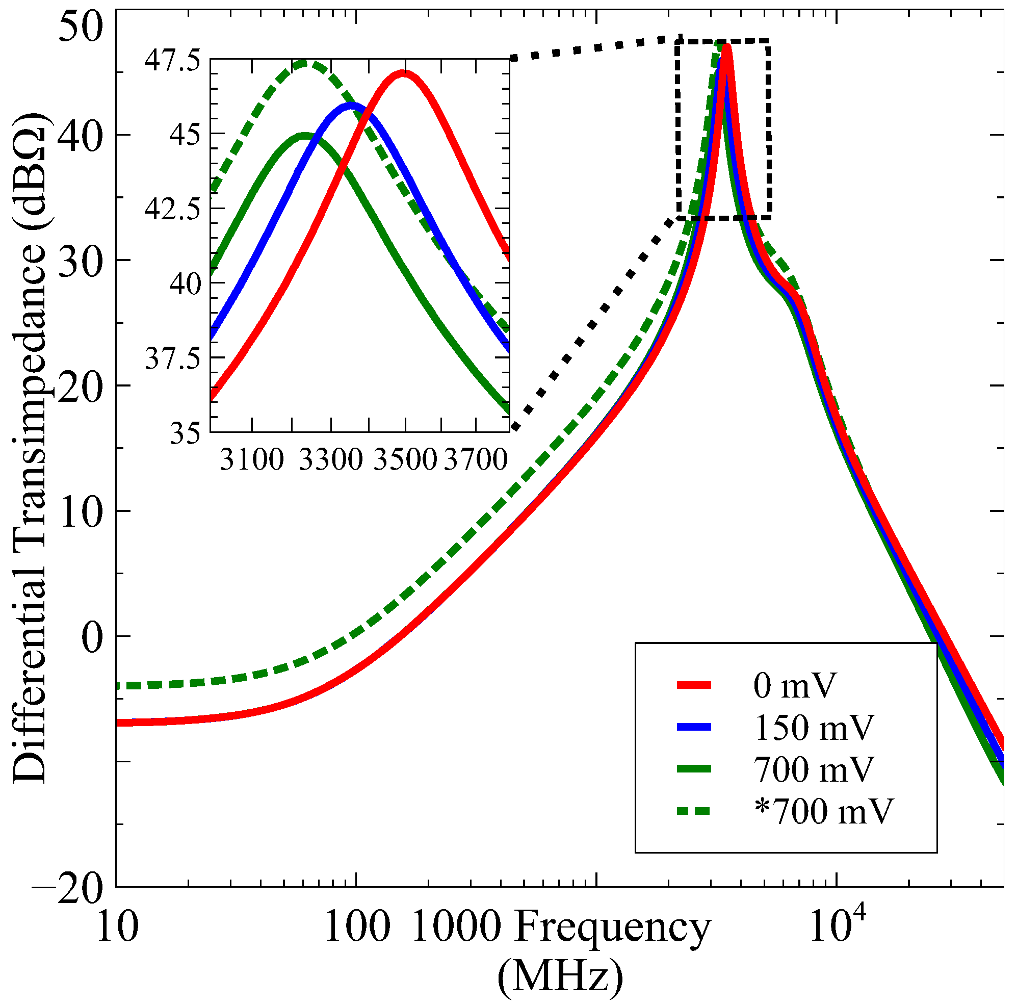
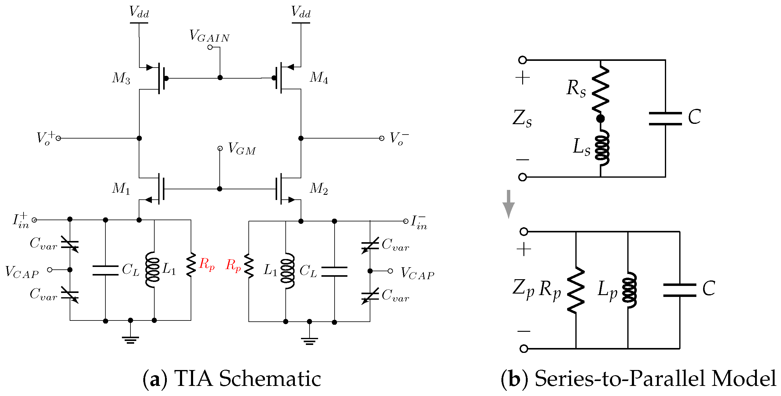
tunability results suggest that the transimpedance gain is a function of the center frequency. This coupling is attributed to the non-idealities of the passive components. The parasitic resistances of both the inductor and capacitor contribute to an overall lumped parallel resistance
.
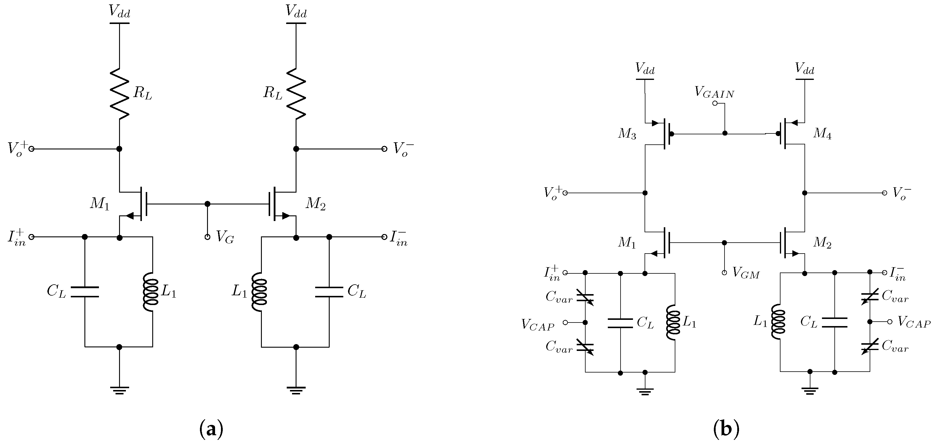
Figure 13b illustrates the transformation of these losses into the equivalent parallel resistance
.
Figure 13a shows the updated TIA schematic with these parasitics. A symbolic analysis of this circuit reveals a bandpass response characterized by the following expressions:
To evaluate the impact of these non-idealities, we consider the limits as the components approach the ideal case (
):
These limits align with the theoretical maximum gain and minimum bandwidth for the studied topology. In practical scenarios where
is finite, the gain is reduced while the bandwidth increases. This is most evident when decomposing the bandwidth expression:
The presence of
introduces an additive term,
, which broadens the bandwidth at the direct expense of peak transimpedance gain. Furthermore, since the inductor quality factor (
Q) is frequency-dependent and optimized for a specific narrow band, operating the TIA at a frequency considerably different from the inductor’s design point can yield significantly lower
Q values. This reduces
, leading to a shallower gain and an even wider, less selective passband. While
accounts for these AC performance trade-offs, the finite stopband gain at low frequencies is specifically caused by the series resistance of the inductor,
. Under DC conditions, the ideal inductor behaves as a short circuit to ground at the source of the common-gate NMOS pair. However, the presence of
prevents a perfect short, resulting in a non-zero voltage at the source and causing a finite, non-ideal low-frequency gain.
4.2. Analysis: Topology Exploration & Synthesis
A promising path for topology discovery involves decomposing a circuit into RLC networks with dependent sources, followed by synthesis back into a transistor-level implementation. Beyond modeling fundamental gain-bandwidth limitations, two-port transistor characteristics, or passive device parasitics, this methodology has proven successful in the discovery of active inductors.
The simulation results underscore the necessity of high-
Q inductors to maintain the selectivity of the bandpass TIA. Consequently, an alternative implementation of the selected topology involves leveraging active inductors. Gyrator-C-based active inductors can achieve quality factors exceeding 100 and self-resonant frequencies (SRF) beyond tens of GHz while significantly reducing on-chip area [
34]. Recent works demonstrate the viability of these components for mmWave and RF applications, including single-ended implementations in 180 nm CMOS [
35] and 65 nm CMOS [
36]. Notably, Schmitz et al. propose a differential Gyrator-C active inductor with an 18 GHz SRF in 65 nm CMOS [
37]. However, it is important to note that active inductors have higher power consumption and require precise frequency tuning to remain effective for the target application [
38].
4.3. Next Steps: Circuit Sizing Strategies
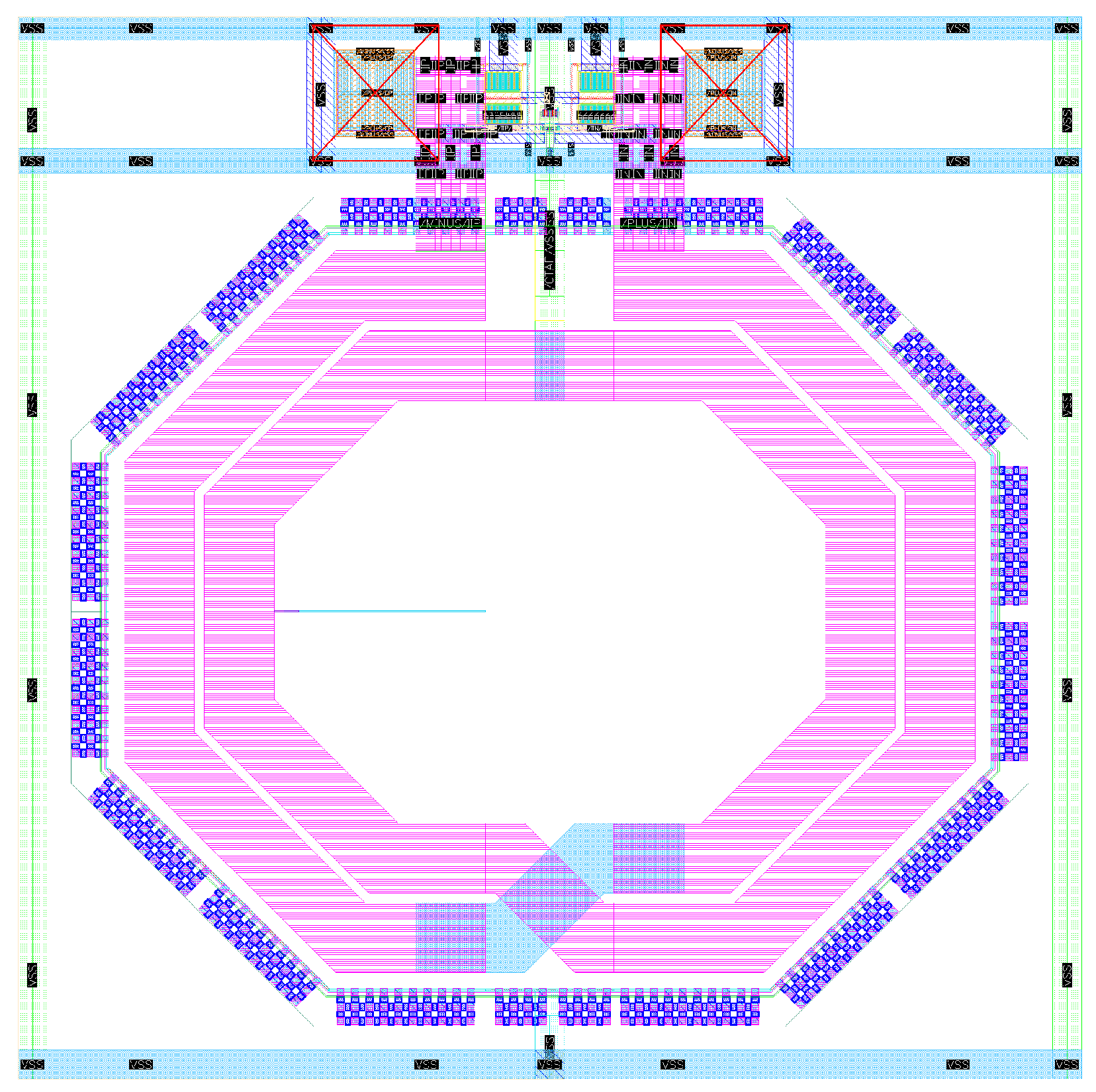
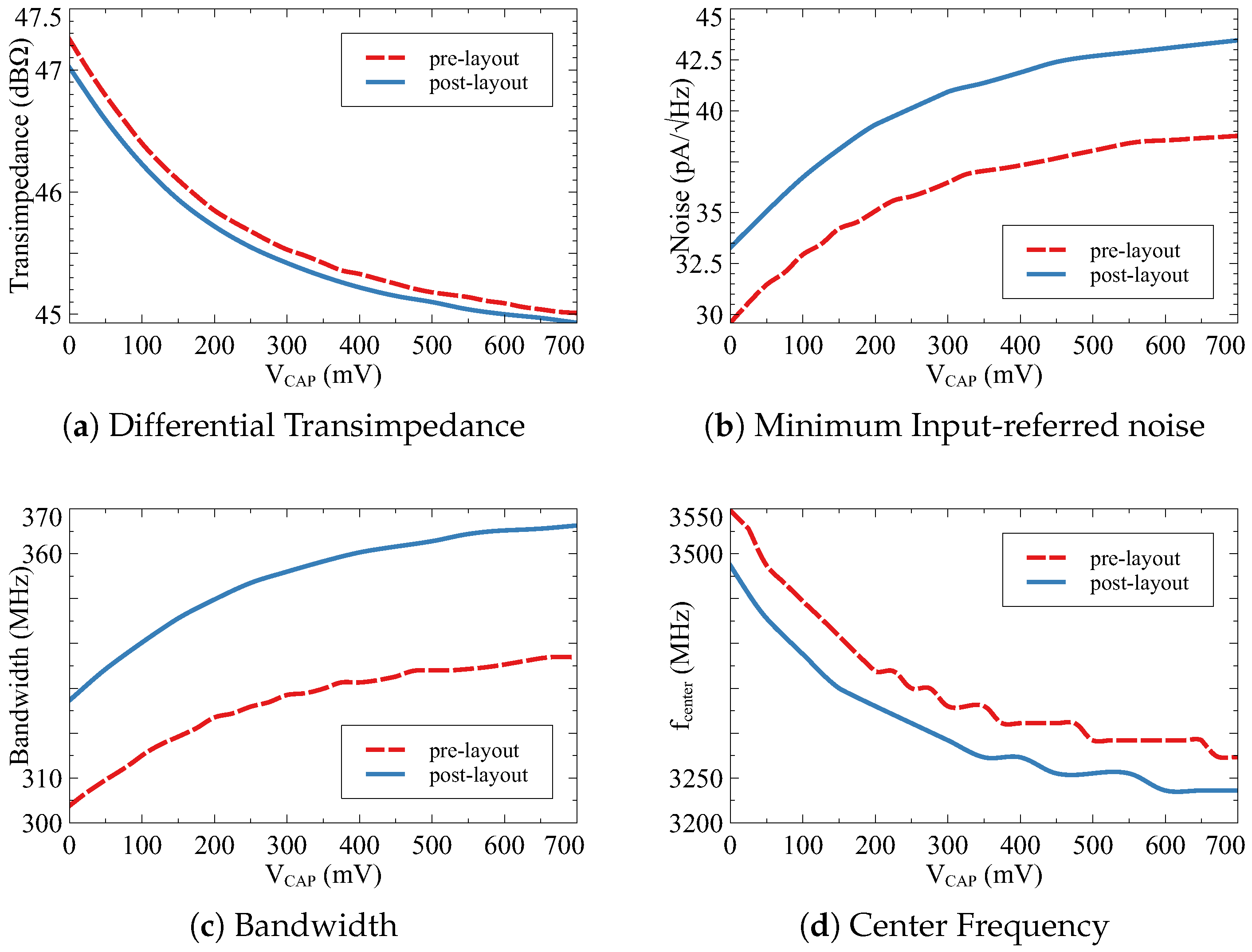
The TIA case study demonstrated that layout parasitics significantly affect performance, requiring schematic-level co-optimization. Future development of SymXplorer will focus on tools that characterize performance boundaries and sensitivity to layout-induced non-idealities, rather than identifying single-point solutions.
Achieving this requires integrating automatic layout generation into the sizing loops. This can be implemented via the Berkeley Analog Generator (BAG) [
39], which has been successfully utilized for layout-in-the-loop optimization by Porrasmaa et al. [
40]. Furthermore, BagNet [
41] demonstrates that BAG-based flows can be significantly accelerated by deep neural networks to navigate the layout-aware design space. As an alternative to template-based generators, GLayout [
42] offers a PDK-agnostic framework where Python-based code automates layout construction. To improve the data efficiency of these sizing loops, Budak et al. proposed a multi-fidelity layout-aware framework that employs Bayesian Neural Networks to approximate circuit performance using fewer training points [
43]. Similarly, Huang et al. [
44] proposed a nested multi-fidelity modeling approach within a Bayesian optimization framework, which strategically uses low-fidelity schematic data to guide the search and minimize the number of costly high-fidelity post-layout simulations.
To further improve the sizing process, technology-specific data should be integrated into the engine. This includes tracking transistor operating points and employing the
methodology to reduce problem dimensionality and maintain physical feasibility within the target process node. Finally, the optimization suite could incorporate reinforcement learning (RL) agents to complement existing stochastic optimizers; tools like AutoCkt [
45] and trust-region RL frameworks [
46] have shown that these agents excel at capturing complex parasitic effects and simplify porting designs across technology nodes.
4.4. Next Steps: Workflow Enhancement with Agentic AI
The current implementation of SymXplorer demonstrates the power of symbolic exploration in discovering high-performance topologies. However, the next evolution of this framework lies in the integration of Agentic AI workflows. An agentic framework can act as a “silicon architect,” where a collection of specialized agents supervises the entire design flow, autonomously leveraging a toolset that includes symbolic exploration engines, circuit optimizers, SPICE simulators, and automatic layout generators.
The following enhancements represent a roadmap for adding agentic intelligence into the design loop:
Intelligent Constraint Synthesis and Topological Expansion: Beyond simple annotation, agents can autonomously parse discovered topologies to identify functional sub-blocks (e.g., current mirrors, differential pairs) and apply constraints for symmetry, ratios, and consistency. Furthermore, an agentic framework can actively propose topological variations to meet stringent specifications; for instance, swapping passive inductors for various active inductor implementations to save area, or dynamically inserting frequency compensation schemes (e.g., Miller compensation or zero-canceling resistors) to stabilize high-gain stages.
Knowledge-Driven Initialization: By leveraging a fundamental understanding of circuit theory and previous discovery iterations, the AI can suggest optimized starting point values for the optimizer. Such “warm-starts” have been shown to significantly improve convergence speed and the quality of the final design results [
47].
Multi-Agent Tool Supervision: A multi-agent system can supervise the execution of diverse EDA tools. For instance, a “Manager Agent” coordinates between the symbolic solver and SPICE simulator, while specialized “Analyst Agents” interpret simulation waveforms to suggest topological refinements or specific device-sizing adjustments.
Resource-Aware Decision Making: A key advantage of an agentic workflow is the strategic invocation of “expensive” computational tasks. The AI evaluates the maturity and performance of a candidate design before committing resources to time-intensive simulations, such as layout generation and parasitic extraction [
48].
By shifting these heuristic and administrative tasks to an agentic layer, the designer can move from manual “tweaking” to high-level architectural oversight, significantly reducing the Time-to-Market for complex analog and RF ICs.