1. Introduction
Technological advances within the telecommunications industry have accelerated in recent years, marked by the transition from previous network generations to the current 5G standard. Within this fifth-generation (5G) ecosystem, services such as ultra-reliable low-latency communication, enhanced mobile broadband, and machine-type communication have emerged, each with distinctive requirements and characteristics [
1,
2,
3]. Building on these advances, the development of wireless technologies has led to a radical transformation in services such as mobile telephony, satellite television, the Internet of Things (IoT), and autonomous vehicles, among others [
4,
5]. However, the radio spectrum below 10 GHz is becoming increasingly saturated, severely limiting the expansion of new applications that require both high data rates and low latency [
6].
Millimeter-wave (mmWave) bands above 20 GHz offer an alternative with higher bandwidths, particularly at 28, 38, 60, and 71–76 GHz [
7]. These frequencies have proven viable in 5G networks for wireless backhaul, fixed access, and ultra-high-speed cellular communications [
6]. Looking ahead to 6G, the extensive use of mmWave and sub-THz will enable emerging applications such as extended reality, holographic communications, and massive sensor networks [
8,
9,
10,
11]. Therefore, the spectrum above 20 GHz is consolidating its position as a strategic pillar for the next generation of wireless communications.
The most common transmission media in RF components include rectangular waveguides, coplanar lines, and microstrips, established technologies that are still used in highly complex circuits [
12]. However, at millimeter frequencies, manufacturing in two metal blocks requires precise electrical contact, traditionally achieved by screwing, diffusion, or brazing. These methods are costly and not very scalable, as the small dimensions at high frequencies require extremely strict manufacturing tolerances [
13].
In this context, Gap Waveguide (GWG) technology has emerged as a robust and low-loss alternative for millimeter-wave components, as established by the pioneering work of Kildal and collaborators [
14]. Its distinctive advantage lies in avoiding electrical contact between metallic plates by imposing artificial boundary conditions that inhibit parallel-plate propagation. This is achieved by emulating a perfect magnetic conductor through periodic structures such as bed-of-nails and mushroom-type EBG surfaces [
14], which create a controlled bandgap that confines the electromagnetic (EM) field along a metallic groove or ridge [
15,
16]. As a result, GWG implementations, including groove gap (GGW), ridge gap (RGW), inverted microstrip gap (IMGW), and microstrip–ridge gap (MRGW), support quasi-TEM modes with most of the energy propagating in air, substantially reducing conduction losses [
12,
17]. These properties have enabled compact, manufacturable, and broadband filtering and antenna structures, demonstrated in 5G backhaul, radar, and emerging sub-THz systems [
18,
19,
20,
21]. Consequently, GWG has consolidated itself as a scalable and mature platform for developing high-frequency RF components.
This work presents the design of a 30 GHz centered bandpass filter based on GWG technology with resonant posts, intended to offer optimal performance for high-frequency communication applications. The main contributions of this work are as follows:
- (i)
Design of a fifth-order, 30 GHz bandpass filter using GWG technology with resonant posts, intended for low-loss, high-performance millimeter-wave applications.
- (ii)
Development of a systematic methodology covering theoretical design, EM simulation, and practical implementation.
- (iii)
Optimization of parameters (, , ) and application of rounded-corner structures to improve manufacturability and assembly.
- (iv)
Simulation-based validation demonstrating a return loss greater than 20 dB and a relative bandwidth of 4.95%, in close agreement with theoretical predictions.
Finally, while numerous Chebyshev-based Gap Waveguide bandpass filters have been described in the literature, most existing studies treat synthesis, electromagnetic implementation, optimization, and fabrication feasibility as largely independent stages. In contrast, the novelty of this work lies in systematically integrating these elements into a single, coherent design workflow. Rather than introducing a new filter topology, the proposed approach focuses on bridging the gap between ideal theoretical synthesis and realistic electromagnetic implementation under practical fabrication constraints. In particular, geometric deviations typically introduced in CNC milling, such as rounded coupling openings, are not handled as post-design corrections but are explicitly modeled, analytically compensated, and re-optimized within the design cycle. Furthermore, the methodology emphasizes the interaction among resonator tuning, coupling control, and excitation structures, accounting for frequency shifts and parameter-coupling effects that arise when multiple cavities are assembled. The use of complementary optimization strategies enables efficient convergence while preserving robustness to manufacturability constraints. Through this integrated approach, this work advances the state of the art by providing a reproducible, simulation-based framework that facilitates the practical realization of compact, highly selective waveguide filters, beyond what is typically achieved through isolated synthesis or single-stage optimization approaches.
Related Works
In recent years, multiple bandpass filter configurations in the millimeter-wave band based on GWG technology have been explored due to their ability to operate without direct electrical contact, thereby reducing conduction losses and simplifying assembly. The first work was developed by Zaman et al. [
22], who proposed a third-order Chebyshev filter at 42 GHz in a ridge Gap Waveguide (RGW). Although the simulation results were promising, the fractional bandwidth obtained was limited. Subsequently, Al-Juboori et al. [
23] presented a bandpass filter in groove Gap Waveguide (GGW) with non-adjacent couplings, generating transmission zeros that improved selectivity at 35.65 GHz, albeit at the cost of a greater manufacturing complexity.
Several efforts have focused on improving miniaturization and selectivity. In [
24], the authors developed dual-mode filters in microstrip–ridge GWGs (MS-RGWs), achieving compact resonators with low insertion losses, demonstrating viability in low-cost PCBs. Complementarily, ref. [
25] describes the design of reconfigurable filters operating between 28 and 33 GHz using additive manufacturing, which promotes low-cost, high-precision solutions for rapid prototyping applications.
In addition to these advances, several studies have investigated bandpass filter topologies based on cavities loaded with pins and resonators coupled by irises, both in conventional structures and in Gap Waveguide configurations. The work presented in [
26] introduced hollow rectangular guide cavities loaded with metal pins, experimentally demonstrating strong spurious band suppression while maintaining low losses within the passband. This approach confirmed the effectiveness of pin-loaded resonant cavities in achieving high-Q passband responses, although the resulting fractional bandwidth remained small. In [
27], a different approach was explored, where pin-loaded resonant elements were integrated into a W-band slot antenna to achieve a dual-band filtering response. The two measured passbands, centered approximately at 76 GHz and 104 GHz, validated the feasibility of using resonant posts for multiband applications in the sub-THz range, albeit with higher insertion losses due to the radiating nature of the structure and the high manufacturing tolerances typical of W-band frequencies. In the context of GWG technology, the study by [
28] investigated a GGW bandpass structure using inductive iris coupling, with a primary focus on characterizing the multipactor phenomenon under high-power operation. Although the design achieved a moderate bandwidth and satisfactory return loss, its objective was not to miniaturize the filter or increase selectivity, but rather to understand the mechanisms of RF breakdown in GGW cavities. A fundamental contribution to the development of GGW filters was presented in [
29], where one of the first experimentally validated GGW bandpass filters was proposed. The design employed a fourth-order Chebyshev topology centered at 40 GHz using inductive irises to control coupling, and demonstrated a measured FBW of approximately 2.5% with an insertion loss close to 1.1 dB. Although valuable, this work did not incorporate loading via resonant posts or consider manufacturing deviations such as pin width errors, which can significantly affect performance at mmWave frequencies. Overall, these works confirm the maturity of both pin-loaded resonators and iris-coupled resonators for mmWave filtering applications. However, they also highlight that most existing designs do not explicitly incorporate realistic manufacturing constraints or optimize post geometries for compact, high-selectivity responses in Ka-band GWG platforms.
Likewise, printed solutions have been explored, as described in [
30], where a Ka-band filter based on a printed ridge GWG (PRGW) was proposed, achieving losses of less than 1 dB with high selectivity. More recently, Gao et al. [
31] presented a 3D-manufactured multiband filter in a GGW, with TE102 and TE201 resonators that enabled a triple-band response in a compact structure. Similarly, in [
32], the authors introduced a Chebyshev filter in a GGW for the WR-75 band, with a bandwidth of 3.7 GHz and insertion losses of less than 1.2 dB, validated in both CNC machining and 3D printing. On the other hand, a study on a folded RGW demonstrated an ultra-wide ninth-order bandpass filter, covering 8–18 GHz with a fractional bandwidth of 75% and insertion losses of 0.52 dB [
33]. Similarly, the authors in [
34] presented a 3D-printed W-band (94 GHz) GGW filter, showing how TE10n modes can reduce sensitivity to manufacturing tolerances. Finally, recent work on GWG technologies has demonstrated the existence of compact bandpass/band-rejection filters with low insertion losses suitable for integration into antenna feed networks. In [
32], the authors described compact slot waveguide filters with a measured insertion loss of less than 1.2 dB. Meanwhile, in [
35], the authors evaluated inverted waveguide filters with microstrips, highlighting their applicability to antenna feed networks.
As described above, although GWG technology has shown great potential in reducing losses and simplifying assembly, limitations remain in terms of realistic manufacturing, such as rounded corners, machining tolerances, and geometric deviations. The gaps presented have motivated the development of this work, which proposes the design of a fifth-order bandpass filter centered at 30 GHz with resonant posts in GWG technology, optimized considering practical manufacturing conditions, and validated through high-level EM simulations.
The content of this article is organized as follows.
Section 2 describes the methodology used for the analysis, modeling, and parameter extraction of GWG structures.
Section 3 details the complete design and implementation of the proposed bandpass filter, including the synthesis process, the configuration of the resonant cavity, and the coupling structures.
Section 4 presents the results of the electromagnetic simulation, the optimization procedures, and the comparative analysis of the filter performance. Finally,
Section 5 summarizes the main conclusions and outlines possible directions for future research.
2. Methodology
The methodology adopted for designing the proposed fifth-order bandpass filter in GWG technology follows a structured sequence that integrates classical filter synthesis, EM modeling of post-loaded cavities, and optimization under realistic manufacturing constraints. This combined approach aligns with recent findings indicating that GWG structures are susceptible to machining tolerances and geometric deviations [
32,
34].
First, the resonant behavior of an isolated cavity was characterized by introducing a metal post into the slot region. Similar post-loaded resonators have been successfully applied in both RGW and GGW platforms [
22,
23], demonstrating their suitability for compact, low-loss, and highly selective responses. A modal analysis revealed a nearly linear relationship between the height of the post and the resonance frequency, enabling the initial tuning of the resonators to approximately 30 GHz. Second, a fifth-order Chebyshev prototype was used to obtain the necessary coupling coefficients and external quality factors. These synthesized parameters guided the EM extraction of the coupling between resonators by modifying the effective width of the waveguide, following design principles analogous to the inductive irises commonly used in GWG filters and classic waveguide filters [
29,
30]. After assembling the preliminary structure, full-wave simulations revealed a frequency shift resulting from EM interactions between adjacent cavities and excitation windows. This was corrected by exploiting the previously determined linear dependence between post height and resonance frequency. Next, multi-parameter optimization was performed using the Interpolated Quasi-Newton [
36] and CMA-ES [
37] algorithms, adjusting the pole heights and coupling window dimensions to minimize in-band reflection and transmission ripple. To ensure manufacturability, the model incorporated the geometric constraints associated with the use of a 1 mm milling tool. Rounding the corners of the windows effectively reduces the coupling aperture. Therefore, an analytical compensation was applied by increasing the window length. This step is critical in GWG structures, where slot height, AMC geometry, and discontinuities in transitions strongly influence device performance [
33]. Finally, the complete filter, slot region, cylindrical resonators, compensated coupling windows, and WR28 transitions were validated using full-wave EM simulations. The response obtained met the design objectives: a center frequency close to 30 GHz, an FBW of 4.95%, return losses greater than 20 dB, and selectivity consistent with Chebyshev synthesis, while maintaining compatibility with realistic manufacturing processes [
32,
35].
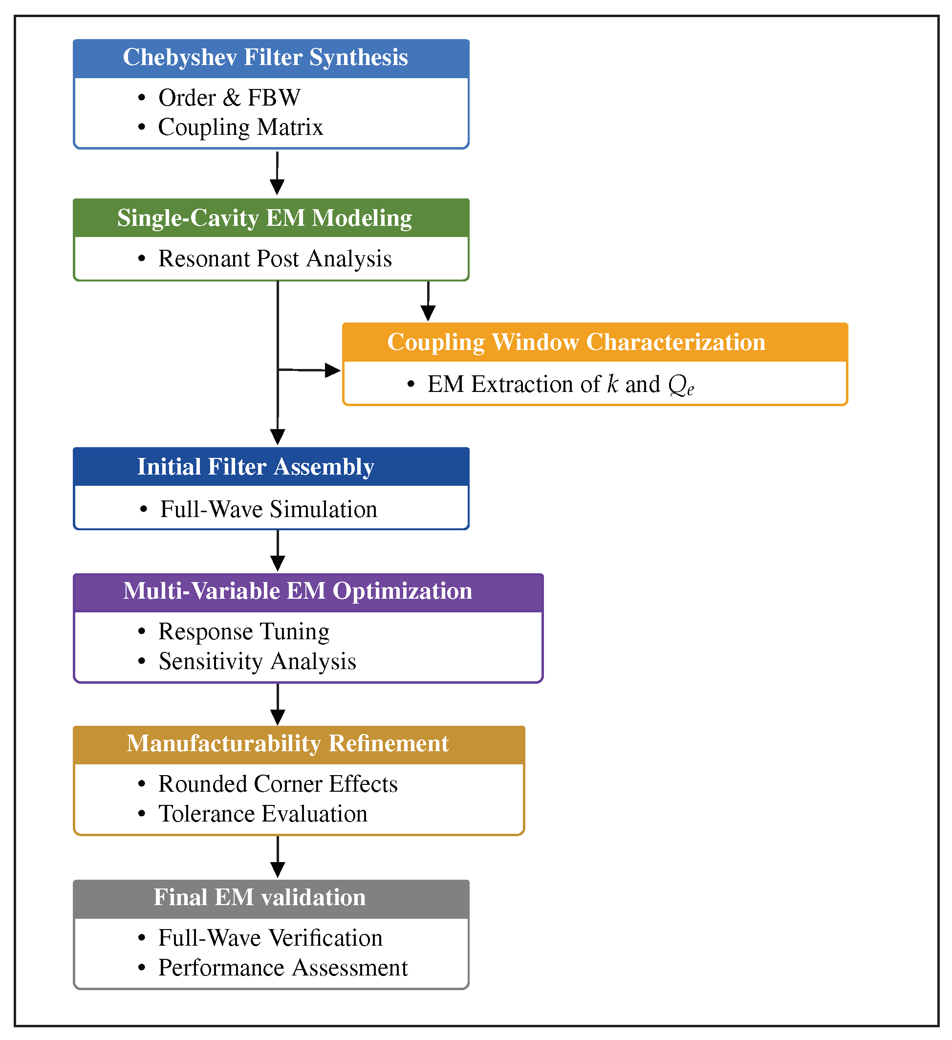
Based on the methodological framework, the following section presents the detailed steps involved in designing the proposed Ka-band GWG bandpass filter. For clarity and readability, the entire design workflow is summarized in a block diagram provided at the beginning of the Design section (
Figure 1). This design provides an overview of the main stages before in-depth technical development.
3. Bandpass Filter Design and Implementation
This section presents a unified description of the design methodology, theoretical synthesis, EM modeling, and physical implementation of the proposed fifth-order bandpass filter. An overview of the complete workflow is provided first to facilitate readability, followed by a detailed technical development of each design stage. The process begins with specifying the electrical requirements and synthesizing an ideal Chebyshev response [
38]. These results are then used as targets for the geometric design of resonant cavities, coupling windows, and external excitation structures, implemented and validated using full-wave simulations in CST Microwave Studio Suite [
39].
Figure 1 shows the block diagram of the proposed manufacturability-aware design for the Ka-band GWG bandpass filter. The flowchart summarizes the main steps of the design flow, starting from Chebyshev synthesis and EM-based single-cavity characterization, followed by coupling window extraction, initial filter assembly, multi-variable EM optimization, manufacturability refinement, and final EM validation. This representation is intended to improve the readability and accessibility of the overall design procedure before detailing each step in the following subsections.
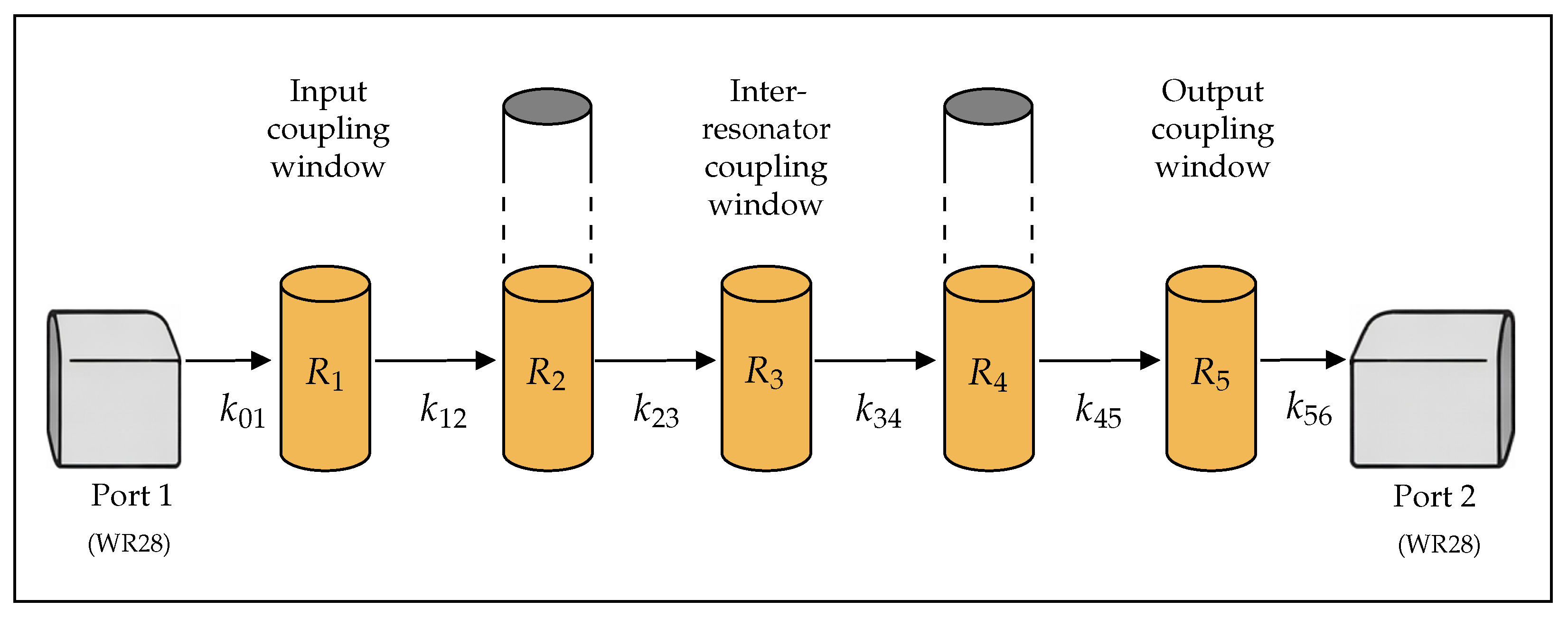
Figure 2 shows a high-level schematic topology of the proposed fifth-order GWG bandpass filter. The diagram illustrates the signal flow from the WR28 input port through the chain of cylindrical resonant cavities and coupling windows, up to the WR28 output port. This simplified representation highlights, at a conceptual level, the correspondence between the ideal Chebyshev synthesis parameters (external quality factors and inter-resonator coupling coefficients) and their physical implementation using resonant posts and inductive coupling windows in the GWG structure.
3.1. Technical Requirements and Ideal Filter Synthesis
The filter is specified to operate within a passband from 29.5 to 31 GHz, with stopband limits between 28 and 32 GHz, a return loss
of 20 dB, and an isolation
of at least 30 dB.
Table 1 summarizes the required electrical parameters.
Based on Equations (
1)–(
3), the resulting parameters are
GHz,
GHz, and FBW
.
A return loss of
dB corresponds to a ripple level of
dB. Based on Chebyshev theory [
38], the minimum order satisfying the selectivity constraint is
. The normalized coefficients for a fifth-order response are listed in
Table 2.
These coefficients enable the computation of resonator couplings, external quality factors , and internal resonant elements required by the equivalent lumped model.
Ideal Circuit Design in ADS
The ideal lumped network consists of five resonators coupled according to the matrix derived from the
coefficients. The coupling coefficients between resonators
and
are calculated using Equations (
4) and (
5):
The resulting coupling values are given in
Table 3. Likewise, the input and output impedances,
and
, are determined in Equation (
6):
Assuming the inductances
nH, where
; the capacitances
follow from the resonance condition defined in Equation (
7), obtaining
pF. Furthermore, Equation (
8) determines
.
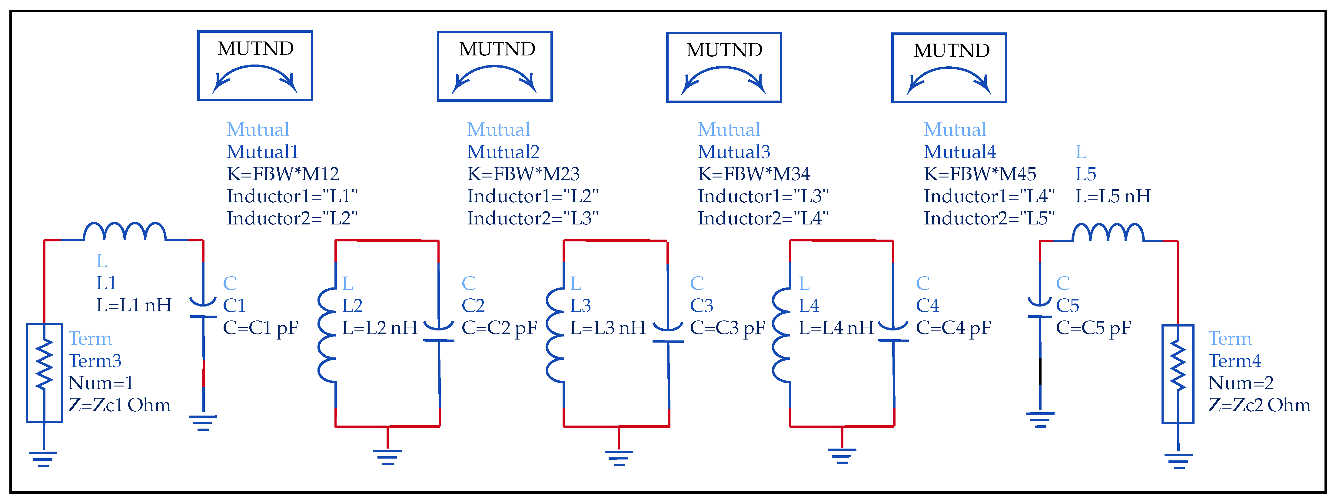
Figure 3 shows the ADS circuit implementation, while
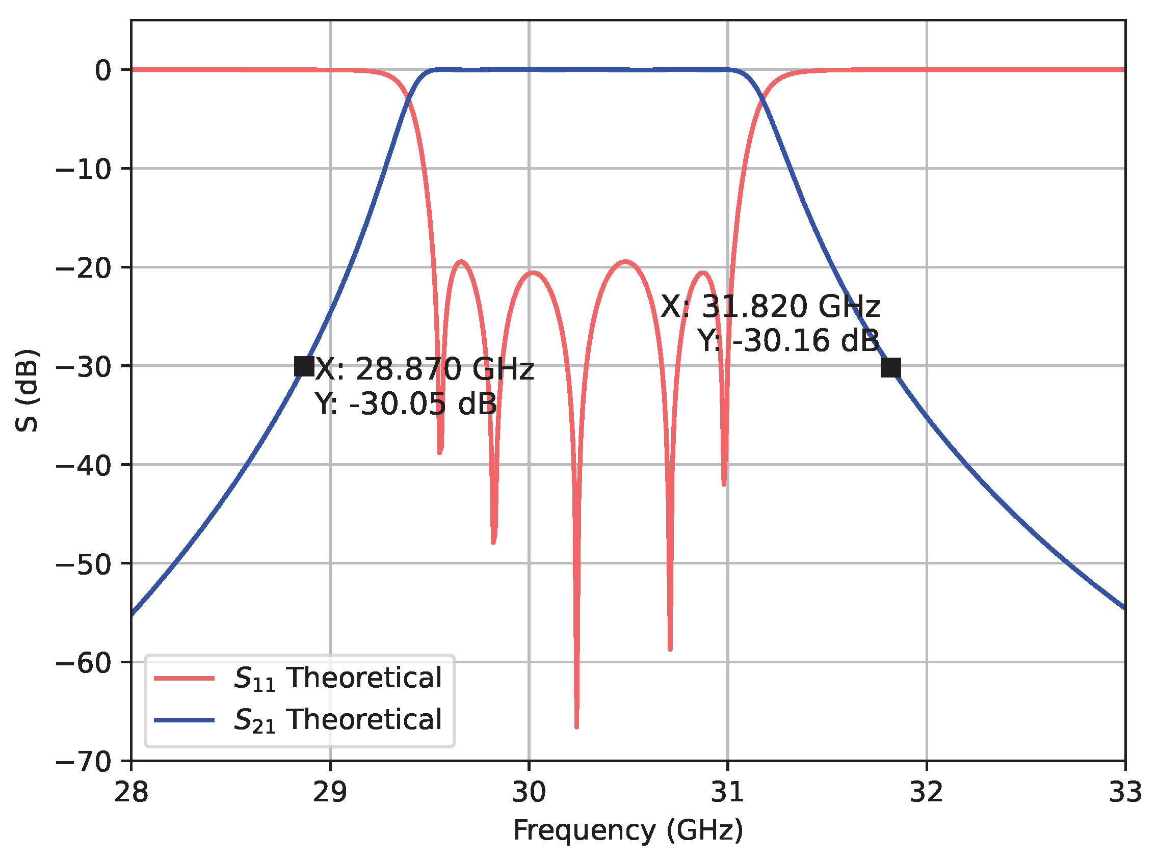
Figure 4 shows the simulated S-parameters corresponding to the ideal Chebyshev filter.
3.2. EM Design of the Resonant Cavity Filter
Once the ideal response and its parameters were obtained, the physical implementation was carried out using periodically loaded metallic posts, which act as an artificial stopband structure. The design focuses on three key stages. First, the definition of the resonant cavity. Second, the synthesis of coupling windows between cavities, and finally, the design of the excitation window to control .
3.2.1. Resonant Cavity Geometry and Tuning
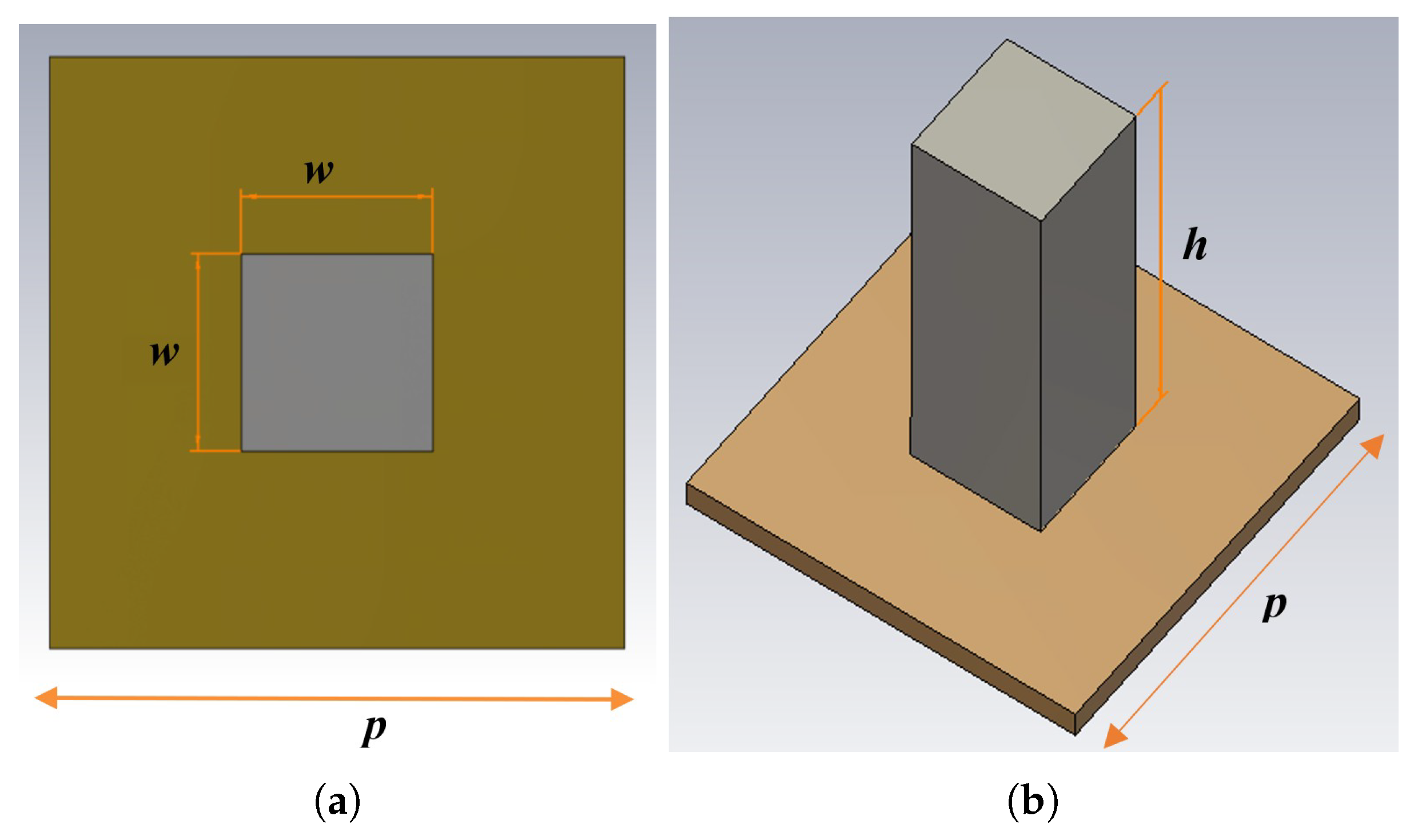
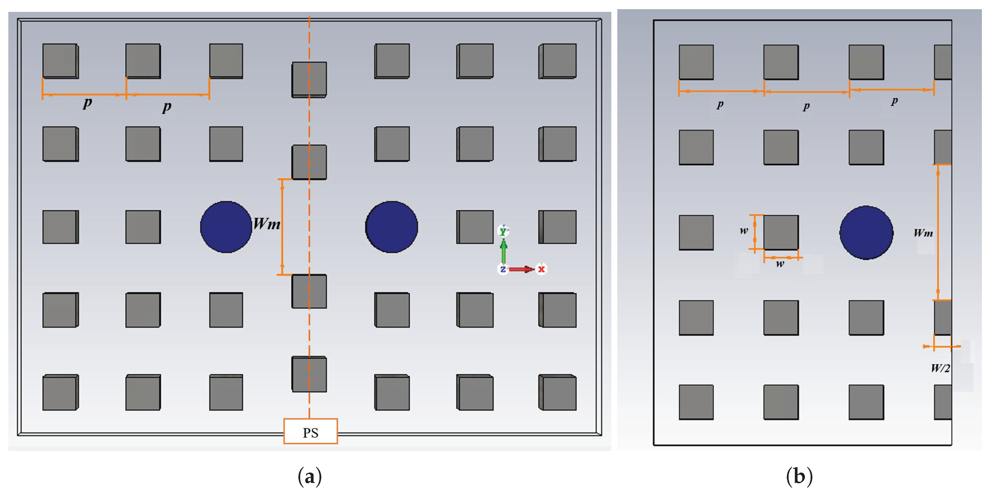
The structure employs a
bed-of-nails periodic surface composed of square posts with dimensions
w,
h, and period
p, shown in
Figure 5. These elements suppress surface-wave propagation and confine the EM fields.
The selected dimensions (
mm,
mm,
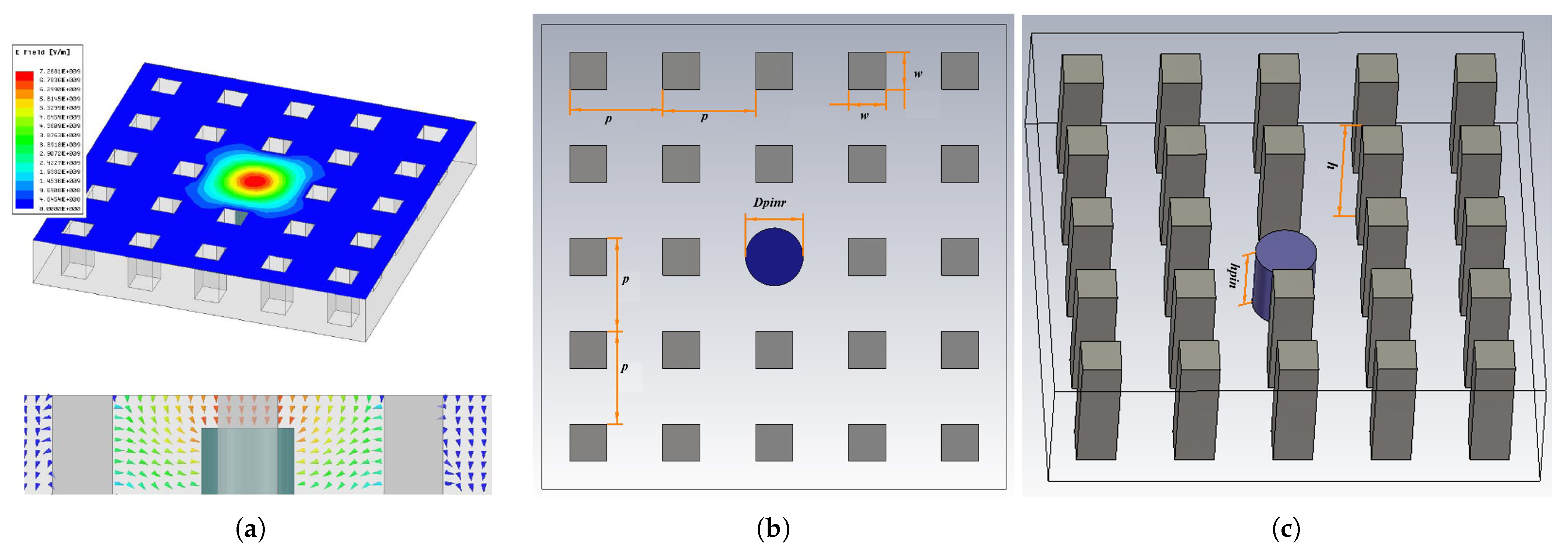
mm) generate a stopband between 28 and 32 GHz. On the other hand, a circular resonant post is placed at the center of each cavity, chosen to minimize corner currents and improve numerical meshing. Its geometry and eigenmode field distribution are shown in
Figure 6.
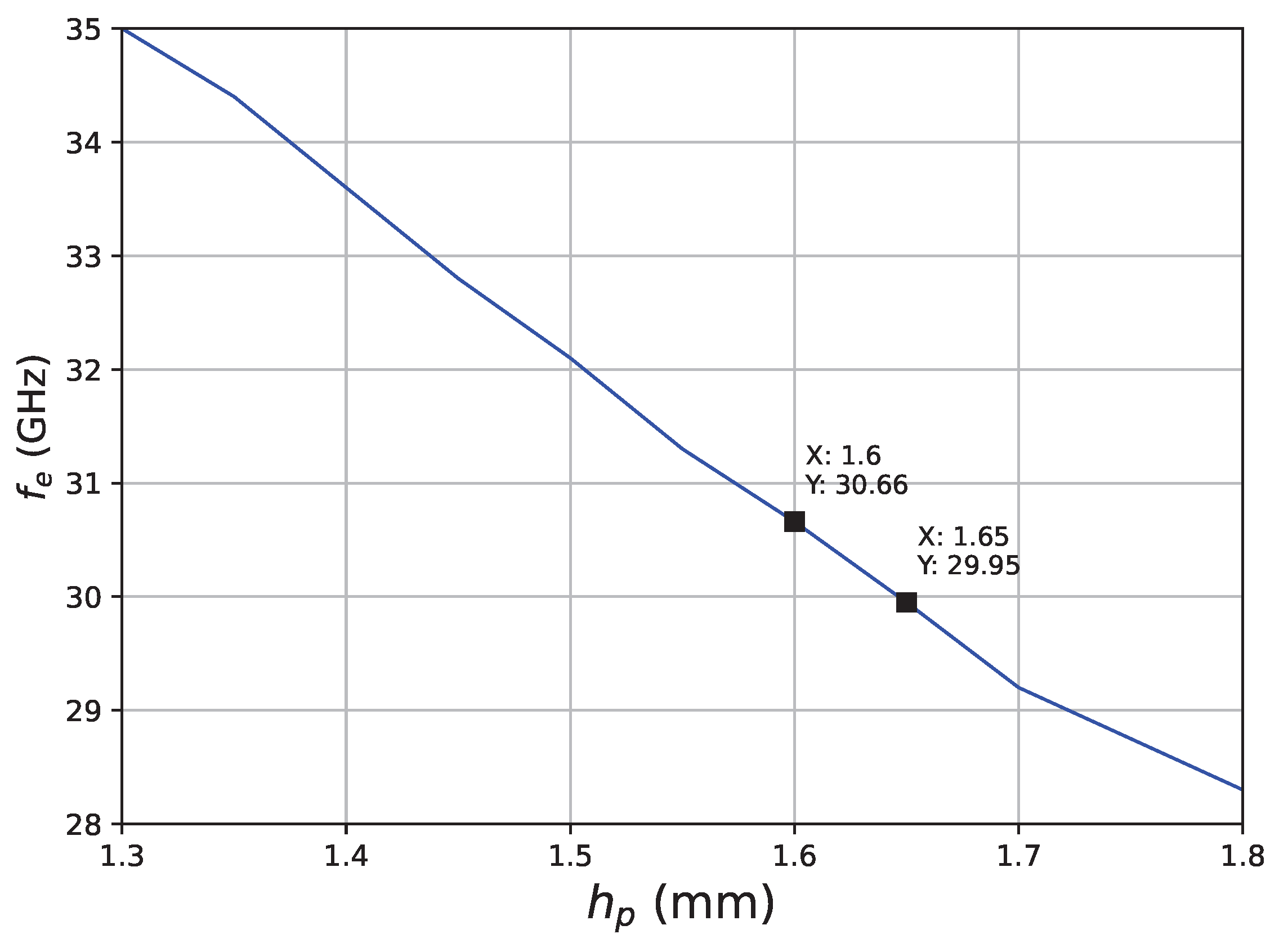
The resonance frequency
depends primarily on the post height
. A sweep between 1.3 and 1.8 mm, refined near the target frequency, produced
mm for
GHz (
Figure 7), where
denotes the resonance frequency of the cavity.
3.2.2. Coupling Window Design
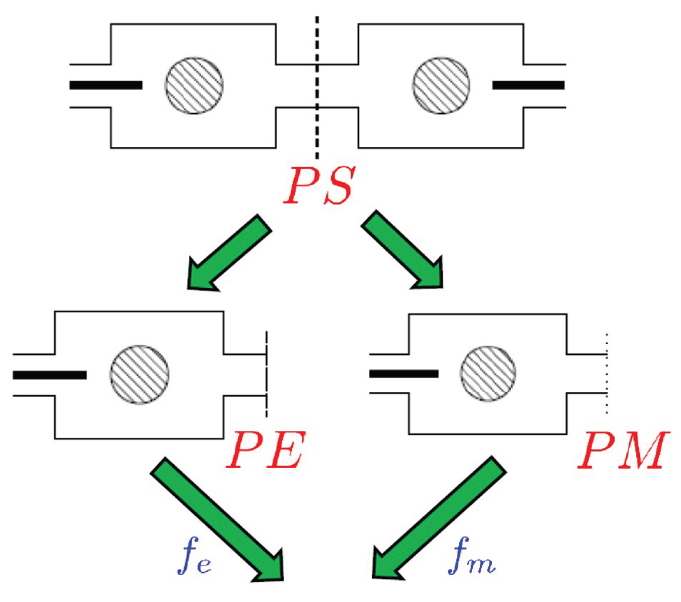
The coupling coefficient
k between adjacent cavities is obtained using a symmetric two-resonator configuration with electric (PE) and magnetic (PM) symmetry planes, illustrated in
Figure 8.
k is calculated by Equation (
9)
where
and
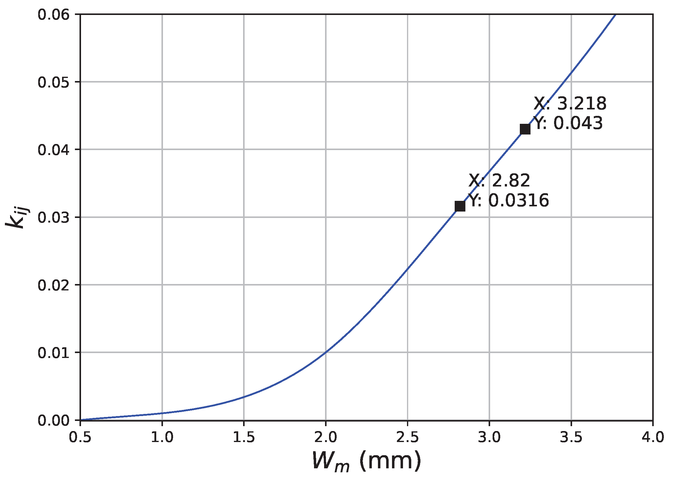
correspond to PE and PM boundary conditions. The coupling window width
controls
k (
Figure 9), where
represents the generic coupling window width used during parameter sweeps.
Figure 10 shows the resulting
curve. Matching these values with the ideal model produces
3.2 mm and
mm.
3.2.3. Input Window and
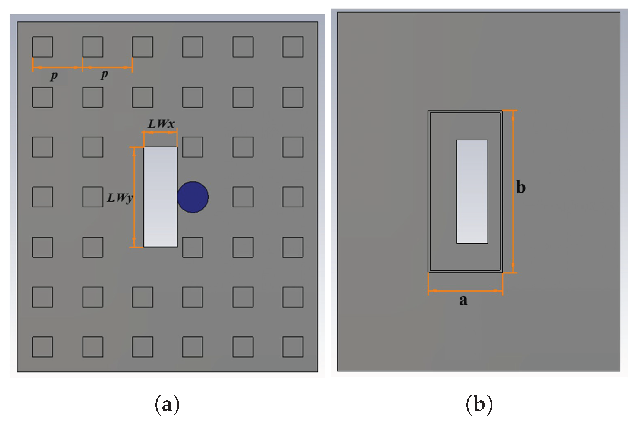
The resonator is excited using a rectangular aperture of size
coupled to a WR28 waveguide, as shown in
Figure 11. The aperture is shown in
Figure 12.
is computed from the phase of
by Equation (
10)
where
is the angular resonance frequency, and the resonance is obtained from the group delay defined in Equation (
11).
Table 4 shows the values from the parametric sweep of
. Finally, the target
is satisfied for
mm.
3.3. Final Filter Implementation
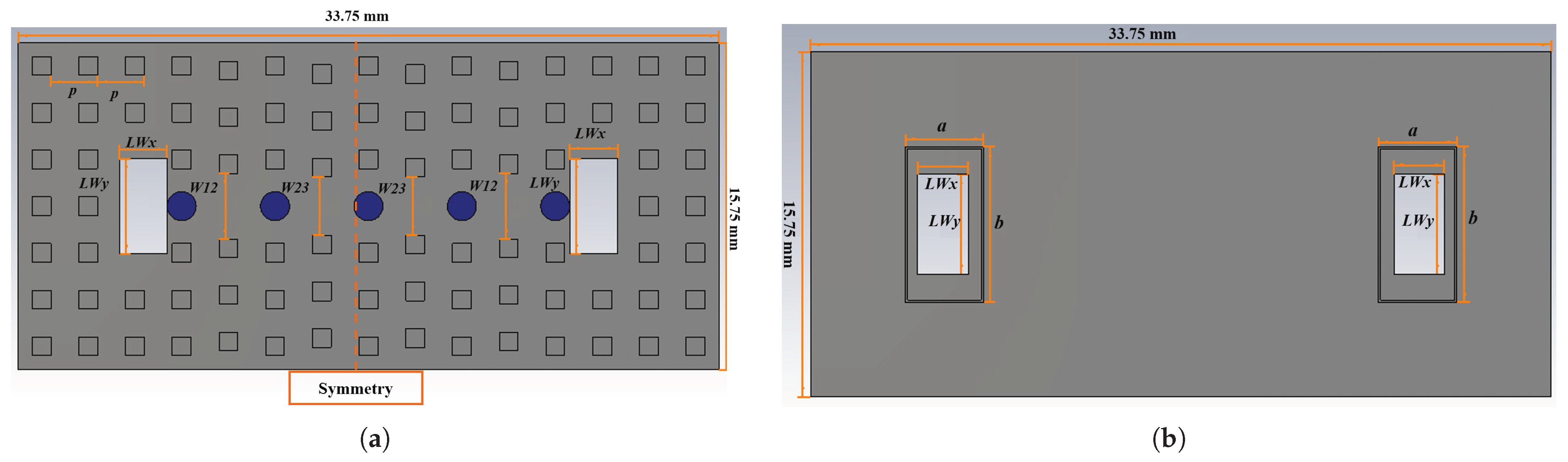
The complete structure consists of five cylindrical-post resonators, coupled through windows of widths
and
and excited through optimized input/output apertures.
Figure 13 shows the front and rear views of the assembled device.
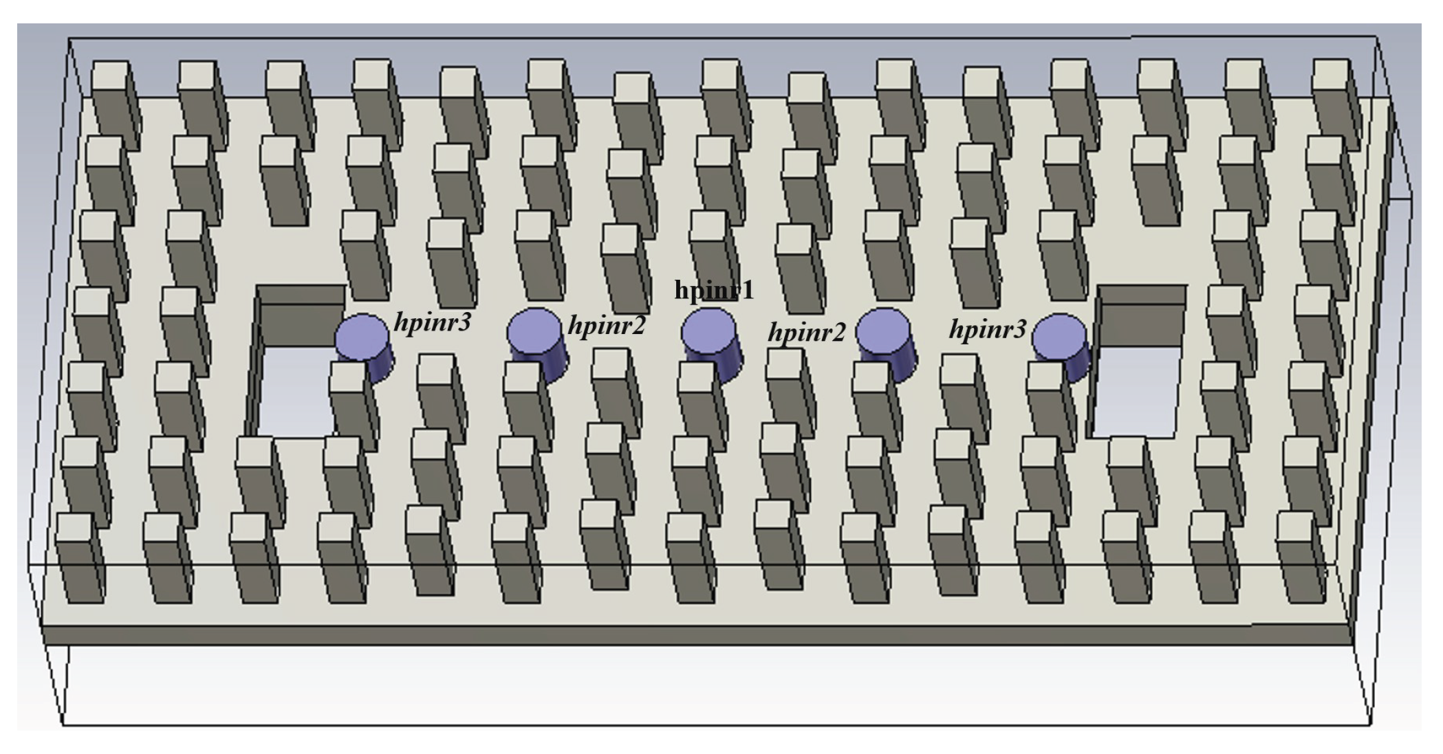
Different resonator heights,
,
, and
, are used to preserve symmetry and compensate for small frequency shifts, as shown in
Figure 14.
4. Results and Discussion
This section presents the full-wave EM results of the proposed fifth-order GWG bandpass filter. The analysis is structured into four stages. First, the initial implementation uses geometrical parameters obtained from the synthesis stage. Second, parametric optimization of coupling and resonant elements is performed. Third, redesign, including realistic, rounded-corner windows introduced by milling constraints, is implemented. Finally, a comparative evaluation against the ideal Chebyshev response is performed.
4.1. Initial EM Simulation
The first EM simulation was performed using the geometric parameters obtained from the resonator, coupling window, and external coupling analyses.
Table 5 summarizes the initial configuration.
The resulting
S-parameters did not match the ideal Chebyshev response: the passband shifted upward from the 29.5–31 GHz region due to interactions between cavities and input/output windows not accounted for in the isolated-resonator analysis. To compensate for this shift, the linear dependence of
on
was estimated from two simulated points (
Figure 7) described in
Table 6.
Based on
Table 6 and Equation (
12), the slope of the linear model was obtained, resulting in
GHz/mm, and subsequently used to estimate the corrected value of
required to place the resonance at 30.24 GHz, resulting in
mm.
4.2. Optimization of Filter Parameters
A multivariable optimization was performed to align the EM response with the ideal coupling matrix. The optimized parameters included the resonator heights (
,
,
), the inter-cavity window widths (
,
), and the external coupling dimension
. Likewise, optimization was conducted using two algorithms available in CST: Interpolated Quasi-Newton and CMA Evolution Strategy (CMA-ES) [
39].
Table 7 summarizes the optimized geometric parameters obtained after full-band EM tuning. The optimized geometry produced an in-band return loss
dB, an insertion loss ripple ≈ 0 dB, and indicated an accurate implementation of the theoretical coupling levels.
4.3. Realistic Implementation Including Rounded-Corner Windows
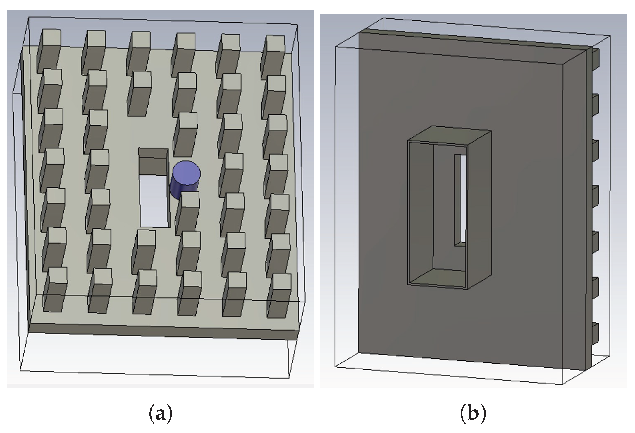
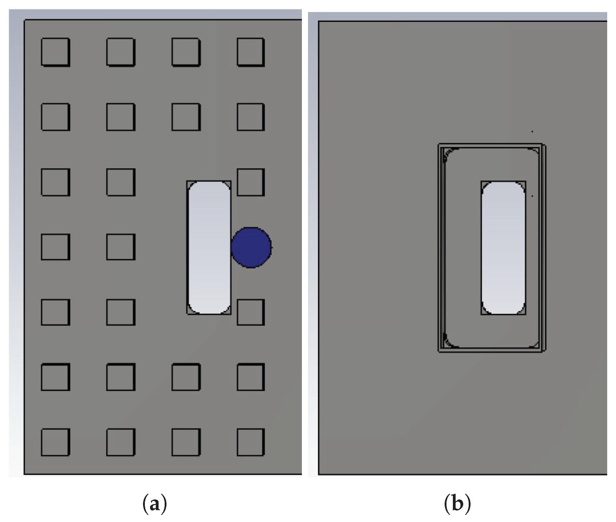
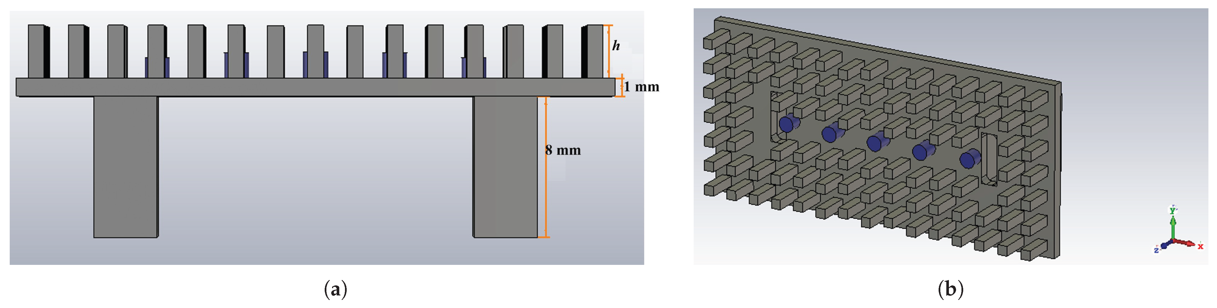
Figure 15 shows the modified geometry. To account for manufacturability using a 1 mm milling cutter, rounded corners were incorporated into the input/output windows.
Figure 16b shows the WR28 excitation interface used in the filter, implemented with an 8 mm waveguide section to ensure adequate field coupling in the first cavity.
Figure 16b shows the complete 3D model of the filter after incorporating the rounded corner transitions.
The introduction of rounded corners slightly reduces the effective window opening. The initial area is calculated using Equation (
13), while the modified area, which takes into account the removed quaternary regions, is obtained using Equation (
14).
Based on the optimized straight-corner values (
mm,
mm), the area reduction is
. Also, to recover the nominal coupling level,
was increased to
. On the other hand, a new EM optimization was performed using this updated geometry. The resulting
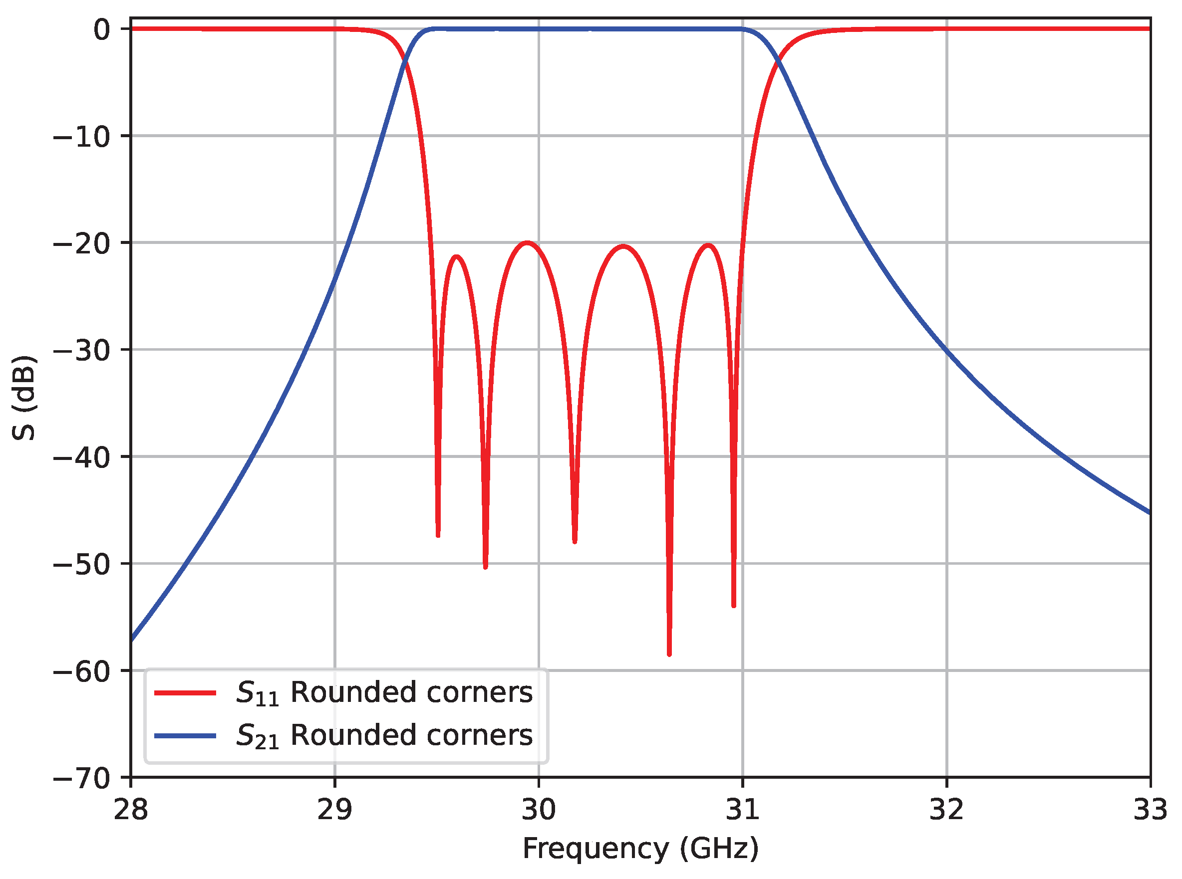
S-parameters, as shown in
Figure 17, confirm that the in-band performance is preserved, maintaining
dB and the desired bandwidth.
Table 8 and
Table 9 summarize the evolution of the geometric parameters throughout the design stages and the computational cost of each optimization procedure.
Table 8 highlights that modifying the rounded corners mainly affects
, while the other parameters remain stable.
Table 9 shows that the CMA-ES algorithm significantly reduced the number of evaluations and the total execution time compared to the Interpolated Quasi-Newton approach.
4.4. Comparison with the Theoretical Response
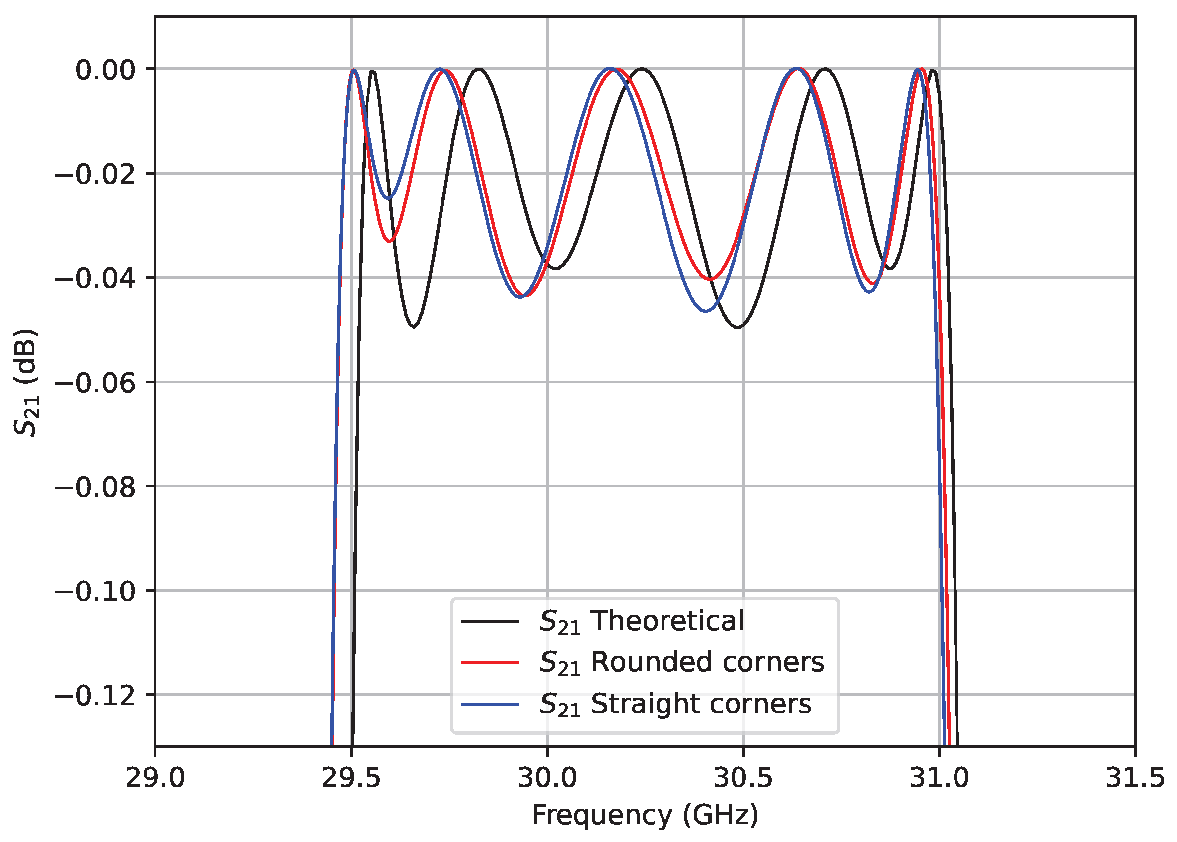
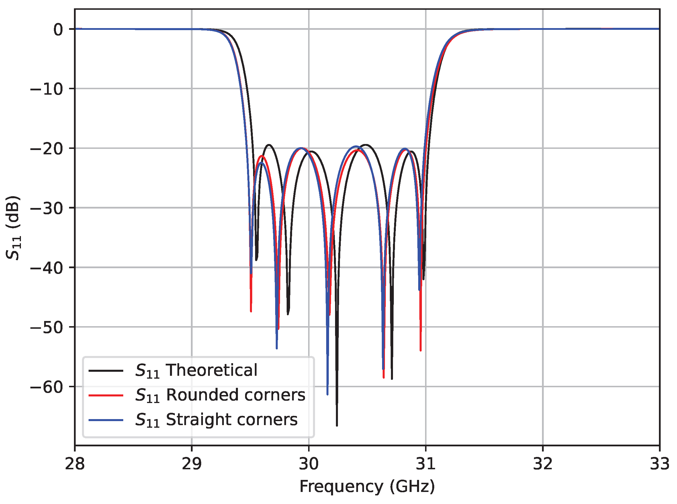
Figure 18 compares the
response of the ideal filter with the two EM implementations. Both physical designs closely follow the theoretical curve, maintaining
dB across the entire passband.
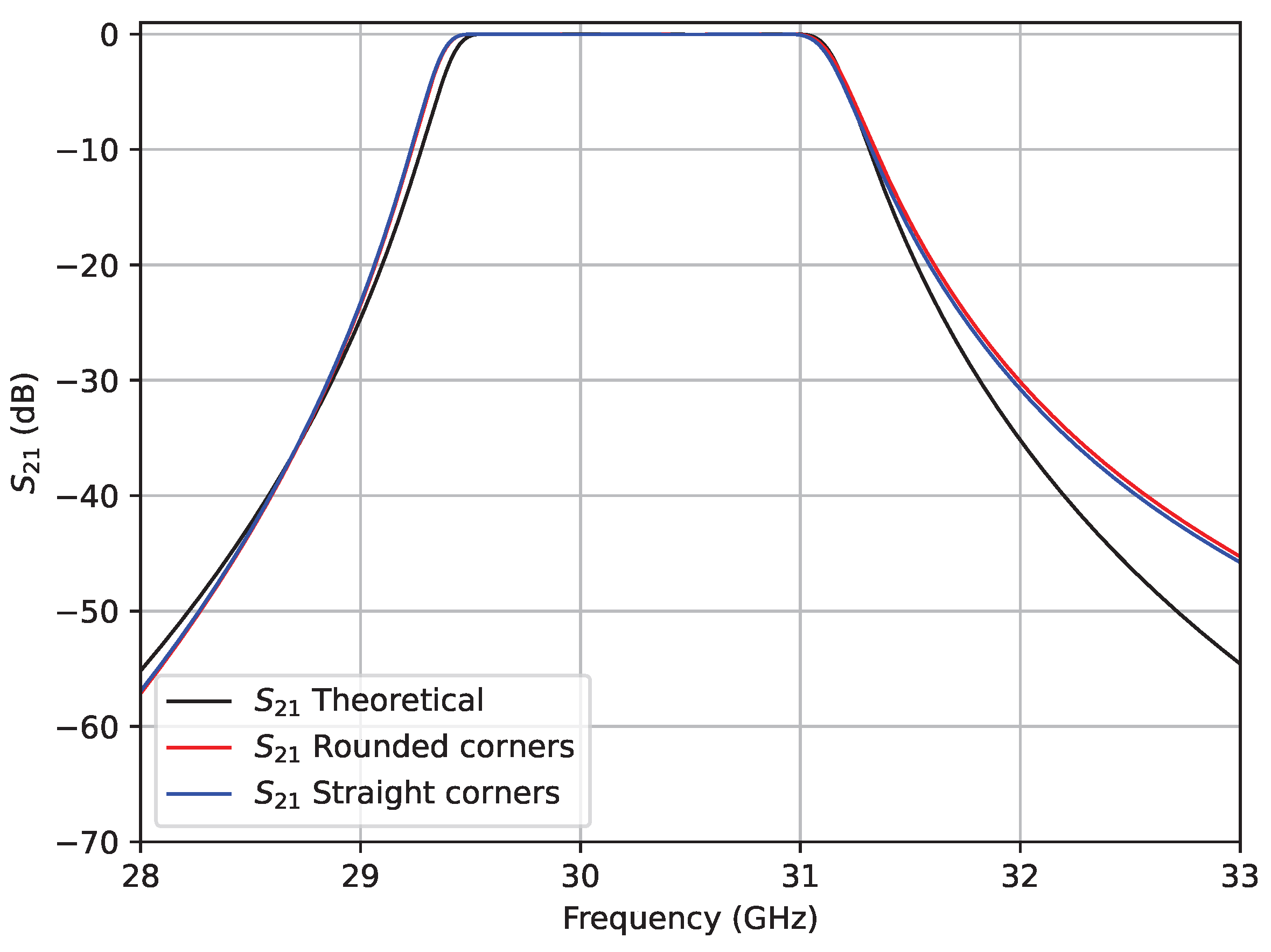
Figure 19 shows that the insertion loss and passband alignment remain constant in all three cases, although the theoretical attenuation slope is approximately 18% steeper in the stopband. This deviation is due to conductor losses, machining tolerances (± 20 μm), and slight variations in the coupling windows.
Finally,
Figure 20 shows the coupling coefficient
r extracted for the ideal filters and those implemented by EM. It can be seen that
r, extracted from the curvature of
, decreases by approximately 9% in both EM models compared to the ideal response, resulting in a small detuning of 0.12 GHz. However, all specifications are still met.
In general, the optimized designs, with both straight and rounded windows, show excellent agreement with the theoretical response. The results confirm that GWG technology, with cylindrical resonant posts and realistically manufacturable apertures, can accurately realize high-selectivity bandpass filters in the Ka band.
4.5. Comparison with Related Works
To highlight the performance of the proposed filter,
Table 10 summarizes several recent works reported in the literature [
22,
23,
24,
25,
30]. The comparison includes
, FBW,
,
, the relative size in terms of wavelength in free space, and the type of validation performed (simulation). In
Table 10, it can be seen that the proposed filter achieves a return loss greater than 20 dB and an FBW of 4.95% at 30 GHz, while maintaining a compact footprint compared to other implementations in GWGs and SIWs. Although only simulation results are currently available, realistic estimates of
indicate competitive performance compared to the state of the art, confirming the robustness of the design methodology and its potential for future experimental implementation.
Furthermore,
Table 10 incorporates three recent contributions that further contextualize the performance of the proposed design. The pin-loaded rectangular waveguide cavities reported in [
26] experimentally demonstrate the ability of metal posts to suppress spurious bands while maintaining low-loss operation. Their passband, measured around 35 GHz, has a bandwidth of approximately 1 GHz, resulting in a narrower FBW compared to this work, albeit with excellent spurious mode suppression and high-quality-factor resonators. Similarly, the dual-band slot array architecture in [
27] integrates pin-loaded resonant structures within a radiating aperture in the W band. The two measured passbands, centered at 76 GHz and 104 GHz, provide effective dual-band filtering, but their insertion loss is inherently higher due to the radiating apertures and high-frequency manufacturing limitations. In the context of GGWs, the multipactor-oriented study in [
28] employs inductive coupling with irises in GGW cavities and includes both simulation and experimental validation in the 17.4–17.5 GHz range. Although the work achieves moderate bandwidth and good return loss performance, its main focus is on characterizing RF breakup in GGW filters, rather than compact, high-selectivity designs. In addition, one of the first implementations of bandpass filters in GGW technology was presented in [
29], where a fourth-order Chebyshev topology centered at 40 GHz was designed and experimentally validated using iris-type inductive couplings. The filter has an FBW of approximately 2.5% and a measured insertion loss of nearly 1.1 dB, with return loss levels ranging from 15 to 18 dB. Although this work effectively demonstrates the viability of GGW cavities and their low-loss operation, it does not incorporate resonant post loading or address manufacturing deviations such as variations in pin width, which can significantly affect high-frequency performance.
Compared to these contributions, the proposed resonant post filter achieves a balance between compactness, selectivity, and return loss while maintaining realistic manufacturing constraints.
As shown in
Table 10, the proposed GWG filter exhibits competitive insertion loss and superior selectivity compared to previous designs, while maintaining a compact volume (approximately
). Unlike other studies, robustness against manufacturing tolerances was verified quantitatively. Also, the improvement in selectivity and compact size shown in
Table 10 is primarily attributed to the use of resonant posts, which allow for stronger electric field confinement and more precise control of the coupling between resonators compared to conventional diaphragms. Furthermore, integrated EM-based optimization allows for the simultaneous adjustment of resonator heights and coupling windows, resulting in an efficient balance between bandwidth, insertion loss, and physical size.
From a practical design perspective, the most critical challenges identified in this study stem from the relationship between resonator heights and coupling window dimensions, which can lead to non-linear frequency shifts near optimal operating points. The optimization process highlights regions of reduced sensitivity that can be exploited to improve robustness against dimensional variations. Furthermore, the results suggest that post-manufacturing adjustment could be facilitated by incorporating tuning elements, such as pins or adjustment screws, placed in locations with lower cross-sensitivity, allowing for controlled compensation without significantly degrading filter performance.
Overall, the results demonstrate that the proposed GWG bandpass filter accurately implements the target Chebyshev response at 30 GHz while maintaining robustness under realistic manufacturing constraints. These findings validate the effectiveness of the proposed design methodology and provide practical insights into the synthesis, optimization, and tolerance-aware implementation of resonant GWG filters in the Ka band.
5. Conclusions
This paper presents the design of a bandpass filter centered at 30 GHz using GWG technology with cylindrical resonators surrounded by periodic bed-of-nails structures. Each stage of the filter was modeled individually to establish relationships between physical parameters and their electrical equivalent, which allowed for a detailed understanding of the resonance and coupling mechanisms between adjacent cavities. Likewise, the input and output structures coupled to a GGW guide were integrated, considering their impact on the overall response of the system. Once the modeling was completed, the fifth-order filter was constructed, incorporating cavities, excitation windows, and rounded corners in the transitions to enhance EM performance. The final optimization stage precisely adjusted the frequency response to achieve the desired theoretical behavior. The results obtained validate the effectiveness of the proposed design; i.e., return losses greater than 20 dB, ripple less than 0.05 dB, and a relative bandwidth of 4.95% around 30 GHz are achieved, demonstrating its viability for applications in 5G communications and high-frequency satellite systems. Finally, a comparison with state-of-the-art implementations confirms that the proposed filter retains a compact size while achieving competitive selectivity and adequate performance (see
Table 10). Furthermore, its demonstrated robustness against dimensional tolerances provides strong evidence of its viability for future manufacturing and practical integration into Ka-band systems.
In summary, this work consolidates a systematic methodology that ranges from ideal synthesis to the inclusion of realistic manufacturing deviations, enabling the design of accurate and manufacturable GWG filters using resonant posts. The demonstrated EM performance and robustness of tolerance support the suitability of the design for upcoming 30 GHz systems, fixed wireless access, and satellite payloads. Furthermore, the approach is scalable to higher mmWave and sub-THz bands, offering a promising foundation for next-generation passive components.
6. Future Work
Although this work focuses on the systematic design and EM validation of a Ka-band GWG bandpass filter, several lines of research arise from the proposed methodology that are left for future investigation. First, experimental validation is a key step to be taken. The manufacture and measurement of a prototype would allow for verification of insertion loss, return loss, and sensitivity to expected machining tolerances, as well as a more accurate assessment of the effects of surface roughness and material conductivity, which are difficult to fully capture in full-wave simulations. Second, a comprehensive statistical analysis of tolerance and sensitivity could be performed. While this work quantitatively addresses specific manufacturability effects, such as rounded corner transitions imposed by milling, a more comprehensive study could be conducted to further explore these issues. Such an analysis, based on Monte Carlo simulations or worst-case tolerance stacking, would provide deeper insight into parameter coupling, performance estimation, and robustness under realistic manufacturing scatter conditions. Third, the strategy of tuning and adjustment after the manufacture of GWG filters with resonant posts deserves further investigation. The strong coupling observed between resonator heights, coupling windows, and center frequency suggests that future designs could benefit from the inclusion of specific tuning elements, such as pins or adjustable screws placed in regions exhibiting reduced cross-sensitivity. These approaches could enable controlled compensation for frequency shifts without significantly degrading overall filter performance. Finally, extending the proposed design methodology to higher mmWave and sub-THz frequency bands represents a longer-term research direction, especially in the context of emerging 6G communication systems. While the underlying principles of GWGs and subsequent resonant designs are, in principle, scalable, operating at frequencies above 90 GHz introduces additional challenges related to tighter dimensional tolerances, higher conductor losses, surface roughness effects, and advanced manufacturing constraints. Addressing these issues rigorously would require dedicated modeling, manufacturing, and measurement efforts that exceed the scope of the present study.




 ,
,