1. Introduction
The rapid electrification of transportation has significantly increased the demand for efficient and reliable electric vehicle (EV)-charging infrastructures. In particular, high-power DC fast-charging systems have become a critical technology for reducing charging time and accelerating the widespread adoption of EVs. With charging power levels continuously increasing from several kilowatts to tens or even hundreds of kilowatts, power conversion systems are required to simultaneously achieve high efficiency, high power density, galvanic isolation, and flexible scalability. Consequently, modular converter architectures have attracted increasing attention due to their advantages in power expansion, enhanced reliability, and improved thermal management through the integration of multiple power conversion units [
1,
2,
3,
4,
5]. However, as the charging power increases to the tens-of-kilowatt level, several engineering challenges become increasingly critical. The increased power level leads to higher semiconductor voltages and current stresses, resulting in increased conduction and switching losses as well as thermal management challenges. In addition, fast-charging systems require rapid dynamic response capability to maintain stable voltage and current regulation under load variations and battery charging profile transitions. For modular parallel architectures, effective current-sharing capability is also essential to avoid uneven power distribution and thermal imbalance among individual power modules.
Currently, isolated two-stage AC–DC converter architectures are widely adopted in medium- and high-power EV-charging systems. In these structures, the front-end AC–DC stage is mainly responsible for grid-side power factor correction (PFC), whereas the isolated DC–DC stage provides voltage conversion, galvanic isolation, and battery-charging regulation [
6]. Various combinations of advanced PFC rectifiers and isolated DC–DC converters have been investigated to improve the overall performance of EV-charging systems. Vienna rectifier-based chargers integrated with LLC resonant converters have achieved high efficiency by utilizing soft-switching operation and reducing switching losses [
7]. In addition, totem-pole PFC combined with LLC resonant converters has been explored for compact charging applications [
8,
9]. Furthermore, Vienna rectifier-based dual-active-bridge (DAB) converters employing wide-bandgap semiconductor devices have been reported to further improve efficiency and power density [
10]. However, these cascaded conversion architectures inevitably introduce additional power-processing stages, semiconductor devices, passive components, and intermediate dc-link capacitors [
11,
12,
13]. Consequently, the increased system complexity and volume limit further improvements in power density, reliability, and scalability, particularly for high-power EV fast-charging applications. Moreover, reported two-stage EV chargers generally achieve peak efficiencies within the range of approximately 95–98%, while the additional conversion stage and dc-link components increase system volume and power losses, limiting further improvement of the overall power density [
3]. Therefore, reducing the number of power-processing stages and passive components has become an important research direction for high-power EV-charging systems.
To overcome the limitations of conventional two-stage architectures, single-stage isolated AC–DC converters have attracted increasing research attention because they integrate grid-side power conversion and battery-side galvanic isolation within a simplified power-processing structure [
14,
15]. Various single-stage converter topologies have been investigated for high-efficiency and high-density charging applications. DAB-based converters provide bidirectional power transfer capability and soft-switching characteristics; however, their practical implementation is often constrained by circulating current losses and complex modulation strategies [
16,
17]. Current-fed isolated converters feature continuous input current characteristics and inherent PFC capability, while the high current stress imposed on semiconductor devices and magnetic components remains a challenge for high-power applications [
18,
19]. Resonant converters, such as LLC-based structures, can achieve high efficiency through soft-switching operation, but their voltage regulation capability is highly dependent on resonant parameters and operating conditions [
20]. Other approaches, including bridgeless and capacitor-less converters, have been explored to reduce conduction losses and improve system reliability; nevertheless, they usually require additional switching devices, auxiliary circuits, or more sophisticated control strategies [
21,
22]. Although modular single-stage converters have been investigated for high-power applications, achieving an optimal trade-off among structural simplicity, efficiency, and scalability remains challenging [
23]. In particular, for high-power modular charging systems, achieving flexible expansion capability while maintaining low device stress, fast dynamic response, and balanced current sharing among parallel modules remains an unresolved technical challenge.
Among various single-stage isolated AC–DC converter candidates, SEPIC-based structures have attracted considerable attention due to their continuous input current characteristic, buck–boost voltage regulation capability, and inherent suitability for power factor correction applications. Several SEPIC-derived converters have been investigated for battery charging and isolated power conversion. A bridgeless SEPIC charger with power-decoupling capability has been experimentally validated for low-power applications, while resonant SEPIC converters have also been explored for compact isolated conversion [
24,
25]. However, these studies mainly focus on single-phase or low-power applications and cannot directly meet the requirements of high-power EV fast-charging systems.
To extend SEPIC converters toward higher power levels, three-phase SEPIC-based rectifiers have been further investigated. A three-phase isolated discontinuous-conduction-mode (DCM) SEPIC rectifier achieved a power factor of 0.998 without input current sensing, demonstrating the potential of SEPIC topology for AC–DC conversion [
26]. Another DCM SEPIC converter was developed for high-voltage applications and experimentally verified under different operating conditions [
27]. Nevertheless, DCM operation introduces increased root-mean-square (RMS) current stress and conduction losses, which become critical limitations in high-power applications. Although a 50 kW off-board charger based on multiple isolated SEPIC modules has been reported, its modular configuration relies on a predefined phase arrangement rather than a flexible input/output-parallel expansion strategy [
28,
29]. Therefore, existing SEPIC-based charging solutions still face challenges in simultaneously achieving high-power operation, low device stress, efficient power conversion, and flexible modular scalability, and developing a high-power SEPIC-based isolated AC–DC converter that simultaneously achieves efficient operation across different conduction modes and flexible modular scalability remains an open challenge.
In this paper, a scalable three-phase modular parallel quasi-single-stage isolated SEPIC-based AC–DC conversion architecture is proposed for high-power EV fast-charging applications. The proposed architecture integrates power conversion, high-frequency isolation, and modular scalability within a unified conversion structure. The proposed converter aims to address the aforementioned challenges by achieving simplified power processing, flexible modular expansion, and effective current sharing among parallel power modules while maintaining high efficiency and galvanic isolation. The operating characteristics of the proposed converter are comprehensively analyzed, with particular emphasis on the transition mechanism between discontinuous conduction mode (DCM) and continuous conduction mode (CCM). Furthermore, the modular parallel configuration, current-sharing performance, and efficiency characteristics are experimentally investigated to demonstrate the feasibility of the proposed architecture for high-power applications.
The main contributions of this work are summarized as follows:
- (1)
A three-phase modular parallel quasi-single-stage isolated SEPIC-based AC–DC conversion architecture is proposed, which integrates PFC capability, galvanic isolation, and power conversion functions within a unified conversion cell while eliminating the intermediate dc-link capacitor.
- (2)
The steady-state characteristics and conduction-mode transition mechanism of the proposed SEPIC conversion cell are systematically analyzed. The operating boundaries between DCM and CCM are derived, providing theoretical guidance for high-power operation.
- (3)
The modular operation scalability, current-sharing behavior, and efficiency performance of the proposed converter are experimentally validated. An 18 kW prototype consisting of two parallel modules achieves a peak efficiency of 97.5%, a power factor of 0.999, and an input current THD of 2.55%. Furthermore, the measured peak currents of the two parallel modules are 23.72 A and 23.46 A, respectively, demonstrating effective current-sharing capability under full-load operation.
The remainder of this paper is organized as follows.
Section 2 introduces the proposed three-phase modular parallel isolated SEPIC converter architecture and explains its operating principles.
Section 3 analyzes the steady-state characteristics of the converter, including the DCM/CCM transition mechanism.
Section 4 investigates the modular expansion strategy and current-sharing behavior.
Section 5 presents the control strategy, dynamic performance analysis, and efficiency evaluation.
Section 6 describes the experimental prototype and presents the experimental results.
Section 7 discusses the advantages, limitations, and future improvement directions of the proposed converter. Finally,
Section 8 concludes this paper.
2. Converter Configuration and Operating Principle of the Proposed Architecture
2.1. Overall Configuration
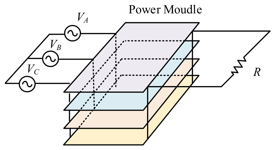
The configuration of the proposed three-phase modular parallel quasi-single-stage isolated SEPIC-based AC–DC converter is illustrated in
Figure 1. Unlike conventional EV-charging systems employing cascaded AC–DC and DC–DC conversion stages, the proposed topology integrates grid-side power factor correction, voltage conversion, and galvanic isolation within a unified SEPIC-based conversion structure.
A hierarchical modular arrangement is adopted, where the fundamental SEPIC conversion cell serves as the basic energy-processing unit. Multiple conversion cells are integrated to form a three-phase conversion module, and multiple modules can be interconnected in parallel to further extend the output power capability. This configuration provides a flexible approach for scaling the charging power while maintaining the same fundamental circuit structure.
The three-phase input terminals are connected in a Δ configuration, enabling each SEPIC cell to directly process the corresponding line voltage of the AC source. Compared with conventional phase-based connection arrangements, this configuration improves the voltage utilization of individual conversion cells and simplifies the expansion of the overall system. Based on this modular concept, higher power levels can be achieved by paralleling multiple identical modules without changing the fundamental conversion cell.
2.2. Isolated SEPIC Conversion Cell
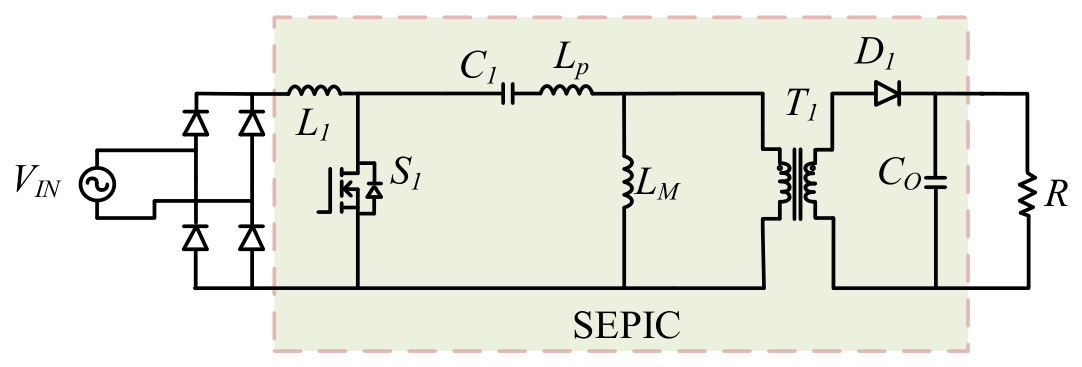
The isolated SEPIC conversion cell, which serves as the fundamental building block of the proposed converter, is illustrated in
Figure 2. The conversion cell consists of an input rectification stage, a SEPIC energy-transfer network, a high-frequency transformer-integrated magnetic component, a secondary-side rectifier, and an output filtering stage.
Conventional isolated AC–DC converters generally employ independent magnetic components and cascaded conversion stages to achieve voltage regulation and galvanic isolation. In contrast, the proposed conversion cell integrates the energy storage function of the SEPIC topology with the isolation function of the high-frequency transformer. This integrated magnetic arrangement enables quasi-single-stage isolated power conversion while reducing the dependence on additional magnetic components.
Benefiting from the inherent characteristics of the SEPIC topology, including continuous input current characteristics, buck–boost voltage conversion capability, and positive output voltage polarity, the proposed conversion cell provides favorable conditions for high-power AC–DC applications. Meanwhile, the high-frequency transformer provides galvanic isolation and participates in the energy-transfer process through its magnetizing and leakage inductances.
2.3. Three-Phase Module Configuration
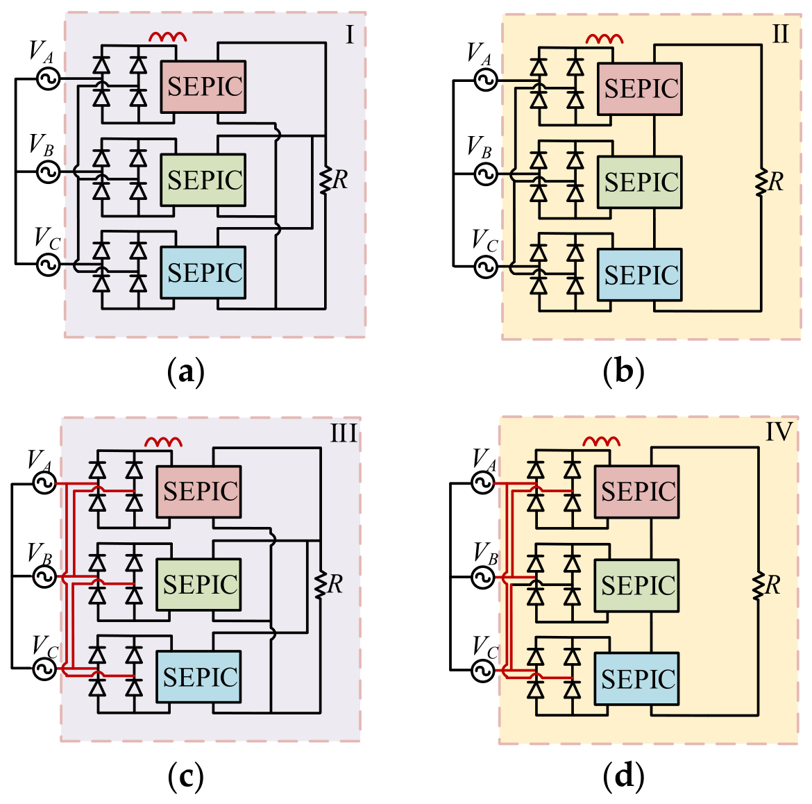
Based on the isolated SEPIC conversion cell, three identical conversion units are integrated to establish a three-phase power module, with each unit connected to one phase of the three-phase AC input. As illustrated in
Figure 3, different module configurations can be obtained by combining various input connection schemes (Y/Δ) with output connection modes (series or parallel).
Among these possible three-phase configurations, the selection of the appropriate input and output connection schemes should consider the voltage utilization of individual conversion cells, current distribution characteristics, and the scalability requirements of high-power EV-charging systems. The Y-connected input configuration applies the phase voltage to each conversion cell, which reduces the voltage stress of individual units but decreases the voltage utilization capability. In contrast, the Δ-connected input configuration enables each conversion cell to directly process the line voltage, improving the utilization of the conversion units under high-power operation.
For the output connection, the series-connected configuration can increase the achievable output voltage by stacking multiple conversion units; however, additional voltage-balancing requirements are introduced among the series-connected units. In comparison, the parallel-connected configuration is more suitable for EV-charging applications with a fixed output voltage, since it enables current sharing among individual conversion units and facilitates modular power expansion. Meanwhile, output-series configurations increase the achievable output voltage but introduce additional voltage-sharing requirements among individual units.
Based on the above comparison, the Δ-input/output-parallel (Δ-IPOP) configuration is selected for the three-phase SEPIC module considering the voltage utilization, current distribution, and modular expansion requirements of high-power EV-charging applications. With the Δ-connected input arrangement, each SEPIC cell directly processes the line voltage of the three-phase source, while the parallel-connected outputs allow the load current to be shared among individual conversion cells. This configuration improves the utilization of individual conversion units and provides a suitable foundation for modular power expansion.
Based on the selected Δ-IPOP three-phase module configuration, further power expansion can be achieved by interconnecting multiple identical modules. For the interconnection of multiple three-phase SEPIC modules, the input/output-parallel (IPOP) configuration is adopted due to the fixed-output-voltage requirement of EV-charging systems. This arrangement maintains the same output-voltage condition among individual modules and increases the overall power capability through current sharing. Consequently, the charging capacity can be flexibly expanded by paralleling multiple identical three-phase SEPIC modules while preserving the basic electrical characteristics of a single conversion module.
2.4. Operating Principle
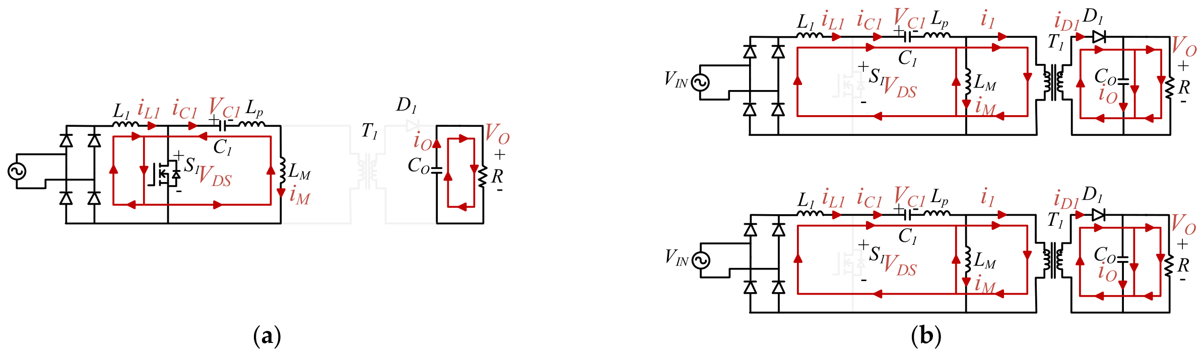
The operating principle of the isolated SEPIC conversion cell is analyzed based on the switching states of the main switch. The operating modes are derived according to the conventional switching-state analysis method for power electronic converters, where the equivalent circuits under different switching states are established to describe the energy-transfer process. Since all conversion cells exhibit identical electrical characteristics, one cell is selected as the representative unit for analysis. As shown in
Figure 4, one switching period consists of two operating intervals corresponding to energy storage and energy transfer.
During the switch-on interval, the input inductor and the transformer-integrated magnetic component store energy from the rectified input voltage, while the secondary-side diode remains reverse-biased, and the output capacitor supplies energy to the load.
During the switch-off interval, the energy stored in the inductive components and the SEPIC energy-transfer capacitor is transferred to the secondary side through the high-frequency transformer, causing the secondary-side rectifier diode to conduct and deliver energy to the output stage.
Through the alternating energy storage and transfer process, quasi-single-stage isolated AC–DC power conversion is achieved within the proposed conversion structure. The detailed steady-state characteristics and continuous conduction mode (CCM)/discontinuous conduction mode (DCM) transition mechanism are analyzed in the following section.
3. Steady-State Analysis of the Proposed Isolated SEPIC Conversion Cell
3.1. Assumptions and Steady-State Modeling
Previous studies have investigated the operating principles, steady-state characteristics, and conduction-mode behaviors of SEPIC-based converters [
25,
26,
27]. These works provide fundamental analysis methods for the derivation of voltage gain and operating boundaries. Based on these principles, the generalized steady-state analysis and CCM/DCM characteristics of the proposed converter are investigated in the following sections. Since the leakage inductance
is much smaller than the magnetizing inductance
, its effect on the steady-state operation and voltage conversion relationship is relatively insignificant. Therefore,
is neglected in the following theoretical analysis.
The input voltage
is expressed as
where
represents the RMS value of the AC input voltage. After the input rectification stage, the voltage applied to the SEPIC conversion cell is expressed as
where
denotes the absolute value operation, which converts the negative half-cycle of the AC input voltage into a positive voltage component.
Since the switching frequency is significantly higher than the grid frequency, the rectified input voltage is assumed to remain constant within one switching period.
The duty ratio of the main switch
is defined as
, and
represents the effective transformer energy-transfer interval. For CCM operation, the energy-transfer interval is equal to the switch-off interval, yielding
whereas for DCM operation,
3.2. Generalized Steady-State Analysis
The steady-state analysis of SEPIC-based converters has been widely investigated in previous studies, where the voltage conversion relationship and operating characteristics are derived based on volt-second balance and charge balance principles [
25].
Under periodic steady-state operation, the volt-second balance of the inductive components and the charge balance of the capacitive elements are applied to derive the steady-state voltage conversion relationship. Although the proposed converter is supplied by an AC input voltage, the switching frequency is much higher than the input frequency. Therefore, the input voltage can be considered approximately constant within one switching period. In addition, the parasitic parameters of the components are neglected in the following theoretical analysis. Under these assumptions, the voltage across the inductive components remains approximately constant during each switching interval, and the current variations of the inductive components can be considered linear according to
. The current variations of the input inductor
, magnetizing inductance
, and SEPIC capacitor
during the switch-on interval of
are expressed as
where
represents the switching frequency,
denotes the rectified input voltage, and
represents the voltage across the SEPIC capacitor.
During the switch-off interval of
, the secondary-side rectifier enters the forward-conduction state, and the energy stored in the magnetic components is transferred to the output side through the high-frequency transformer. The corresponding current variations are expressed as
where
represents the fundamental-period-averaged output voltage, and
represents the transformer turns ratio.
By applying the volt-second balance condition to the inductive components and the charge balance condition to the capacitive elements, the steady-state voltage relationships of the proposed isolated SEPIC conversion cell can be derived as
3.3. CCM/DCM Boundary Condition
The CCM/DCM transition boundary analysis is an important aspect in the design and operation analysis of SEPIC-based converters. Previous studies have investigated the conduction-mode characteristics and boundary conditions of isolated SEPIC converters based on the relationships among inductor currents and converter operating parameters [
27].
The CCM/DCM transition boundary is established based on the relationship between the input inductor current and the magnetizing current. Under the critical conduction condition, the minimum input inductor current is equal to the corresponding magnetizing current, which can be expressed as
Accordingly, the converter operates in CCM when the following condition is satisfied:
The above condition defines the criterion for distinguishing CCM and DCM operation.
3.4. CCM Operation Characteristics
The CCM operating characteristics of SEPIC-based converters have been investigated in previous studies for different applications, including high-frequency and isolated power conversion systems [
25,
28]. Based on the CCM/DCM boundary condition derived above, the proposed converter operating characteristics under CCM operation are further analyzed in this section.
According to the CCM/DCM boundary condition derived above, the converter operates in CCM when the minimum input inductor current remains higher than the corresponding magnetizing current. Under CCM operation, the effective transformer energy-transfer interval
is identical to the switch-off interval. Therefore,
in (5) and (6) can be replaced by
. Based on the steady-state voltage relationship obtained in (7), the duty ratio and current ripple characteristics under CCM operation can be derived as
where
represents the steady-state duty ratio under CCM operation.
Assuming an ideal lossless conversion process, the input power is equal to the output power. Therefore, the switching-period-averaged current of
can be obtained as
where
denotes the equivalent load resistance.
Applying the charge-balance condition of the SEPIC capacitor
, the relationship between the average input current and the magnetizing current can be obtained as
Therefore, the switching-period-averaged magnetizing current can be obtained as
During the turn-on interval of
, the secondary-side rectifier is reverse-biased, and the diode current is zero. The drain current of the main switch is determined by the difference between the input inductor current and the magnetizing current, which can be expressed as
Substituting Equations (10) and (11) into (13), the turn-on current of the main switch can be derived as
During the switch-on interval, the input inductor current increases with a positive slope, whereas the magnetizing current decreases due to the applied voltage polarity across the magnetizing inductance. The corresponding diode current can be derived as
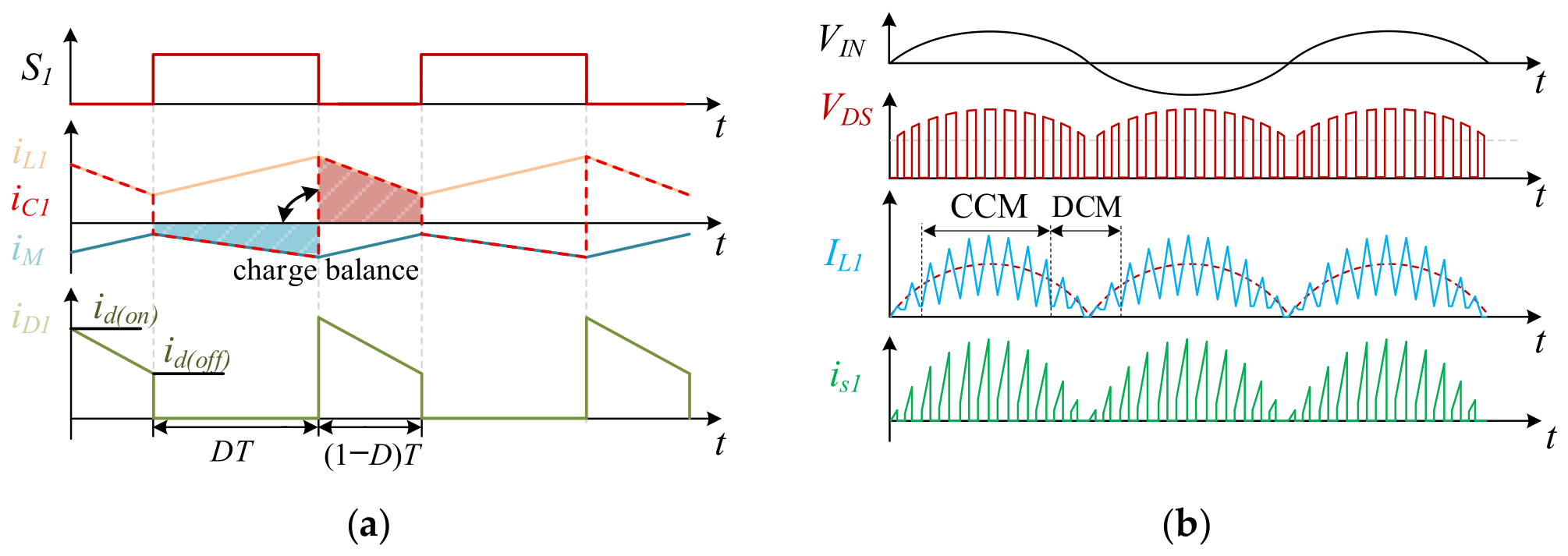
The representative steady-state waveforms under CCM operation are illustrated in
Figure 5. During the switch-on interval, the input inductor current increases with a positive slope, whereas the magnetizing current decreases due to the applied voltage polarity. The capacitor current satisfies the charge-balance condition over one switching period, ensuring zero average current of
. During the switch-off interval, the stored magnetic energy is transferred to the output side through the secondary-side rectifier.
Neglecting the transformer leakage inductance, the drain-source voltage
of
during the turn-off interval can be derived as follows:
The above equations describe the current characteristics of the proposed converter under CCM operation. The CCM boundary condition can subsequently be derived by comparing the minimum input inductor current with the magnetizing current.
By substituting Equations (10), (11) and (13) into the above condition, the critical load resistance required to maintain CCM operation can be derived as
where the equivalent inductance
is defined as
Accordingly, the boundary condition of the input voltage amplitude for CCM operation can be derived as
The above expressions indicate that the conduction mode of the proposed converter is determined by the combined influence of the switching frequency, equivalent inductance, output voltage, load condition, and instantaneous input voltage. The converter operates in CCM when the input voltage amplitude satisfies the derived boundary condition; otherwise, it enters DCM operation.
3.5. DCM Operation Characteristics
The DCM operating characteristics of isolated SEPIC converters have been investigated in previous studies for high-power-factor rectification and high-voltage applications [
26,
27]. These studies provide fundamental analysis methods for understanding the additional zero-current interval and conduction-mode transition behavior of SEPIC converters.
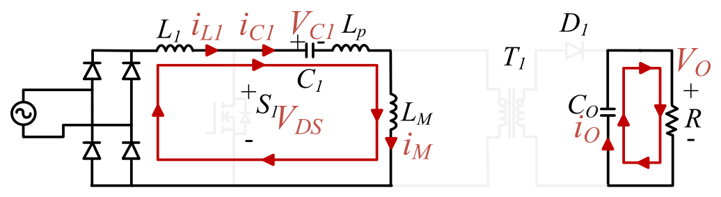
When the operating condition moves beyond the CCM boundary condition derived above, the converter enters the DCM operation region. Compared with CCM operation, an additional zero-energy-transfer interval exists during the switch-off interval of , during which the transformer no longer transfers energy to the output side. Based on the current relationship between the input inductor current and the magnetizing current, DCM operation can be classified into two operating modes, namely, DCM-I and DCM-II.
In DCM-I operation, the input inductor current and the magnetizing current converge during the switch-off interval. The intersection current is defined as
When
, both
and
remain positive after the energy-transfer interval. Therefore, the converter enters the zero-energy-transfer interval, during which the secondary-side rectifier is turned off, and no energy is transferred through the transformer. The corresponding equivalent circuit is illustrated in
Figure 6.
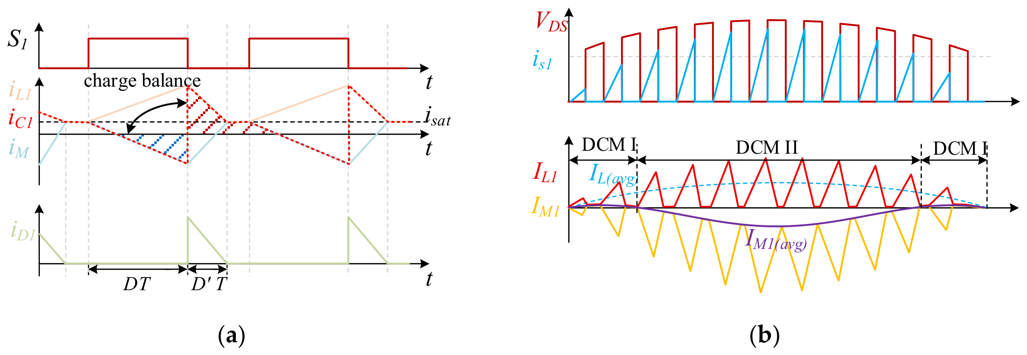
The steady-state current waveforms under DCM-I operation are shown in
Figure 7a. During this interval, the current relationship between the input inductor current and magnetizing current determines the duration of the zero-energy-transfer interval.
Based on the charge-balance condition of
, the intersection current is derived as
The switching-period-averaged input inductor current can be expressed as
By combining Equations (11) and (23), the steady-state duty ratio under DCM-I operation is obtained as
where
represents the steady-state duty ratio under DCM operation.
As shown in
Figure 7b, when the output-voltage condition causes
to become negative, the input inductor current tends to enter the negative-current region. However, the input-side diode bridge imposes a unidirectional current constraint, preventing
from becoming negative.
Consequently, reaches zero before the end of the switching period and remains zero during the remaining interval. This operating condition is defined as DCM-II operation.
Under DCM-II operation, the input inductor current is constrained by the unidirectional conduction characteristic of the input diode bridge. When the theoretical current waveform tends to become negative, the current is clamped to zero during the corresponding interval. Therefore, the average input inductor current should be recalculated by excluding the negative-current interval.
The switch-current characteristics under DCM operation differ from those under CCM operation. Since the input inductor current and the magnetizing current converge before the next switching cycle, the main switch achieves zero-current turn-on. The peak switch current during the turn-off interval is determined by the intersection current and the variation in the input inductor current.
The input current characteristics of the proposed converter are further investigated to clarify its power factor correction capability. Under CCM operation, the input current is regulated through the inner current loop, in which the current reference is synchronized with the input voltage waveform. Consequently, the fundamental component of the input current remains phase-aligned with the grid voltage, thereby achieving a high displacement factor and improved power factor.
For DCM operation, the derived steady-state relationship indicates that the averaged input current exhibits an inherent proportionality with the rectified input voltage under constant-duty-ratio operation. Hence, the proposed converter possesses natural power factor correction capability without requiring an additional input current control loop. Although the DCM II interval introduces a deviation from the ideal current-shaping characteristic, its occurrence is confined to a narrow region around the input voltage zero-crossing points, resulting in limited impact on the line-cycle-averaged input current waveform.
The input current harmonic distortion mainly originates from high-frequency switching ripple, conduction-mode transition, and circuit nonidealities. Since no additional active harmonic compensation scheme is introduced, the THD performance is primarily attributed to the continuous-input-current characteristic of the SEPIC topology and the optimized design of the magnetic components and circuit parameters.
4. Control Strategy and Dynamic Performance Optimization
4.1. Adaptive CCM/DCM Transition Strategy
The CCM and DCM operating characteristics of SEPIC converters have been investigated in previous studies [
26,
27]. However, the adaptive transition mechanism for high-power modular converters has not been fully addressed. Therefore, an adaptive CCM/DCM transition strategy is proposed in this section. Due to the wide operating range and variable-load conditions of high-power EV-charging applications, the proposed isolated three-phase interleaved SEPIC converter is required to maintain stable output regulation and desirable input current characteristics in different conduction modes.
As analyzed in
Section 3, the converter may operate in both CCM and DCM, and the transition between these conduction modes inevitably affects the dynamic performance of the converter. Therefore, an appropriate control strategy is essential to ensure stable operation over the entire operating range.
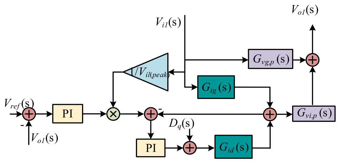
As illustrated in
Figure 8, a dual-loop control structure is employed for the proposed converter. The outer voltage loop regulates the output voltage and generates the reference signal for the inner current loop, whereas the inner current loop provides fast current regulation and improves the dynamic response against input-voltage and load disturbances. Furthermore, by synchronizing the current reference with the input voltage waveform, the proposed control strategy preserves the input-current-shaping capability, thereby contributing to high-power-factor operation.
The controller design is developed based on a control-oriented small-signal model established around the steady-state operating point. The corresponding control-to-current and control-to-voltage transfer functions are subsequently derived and employed for the design of the current-loop and voltage-loop compensators.
Considering the inherent CCM/DCM transition characteristics of the proposed converter, an adaptive mode transition strategy is further introduced to achieve smooth conversion between different conduction modes. By identifying the instantaneous conduction state and adjusting the corresponding control variables, the proposed strategy ensures smooth mode transition and prevents abrupt variations in the duty ratio during CCM/DCM conversion.
4.2. Control-Oriented Small-Signal Modeling
To derive the dynamic characteristics required for controller design, a control-oriented small-signal model of the proposed converter is established based on the averaged state-space modeling approach, which is a widely adopted method for analyzing the dynamic behavior of switching converters [
24]. The detailed derivation of the state-space equations is provided in
Appendix A.
Based on the developed small-signal model, the corresponding control-to-state and disturbance transfer functions are defined as
where
characterizes the duty ratio-to-inductor current dynamics and serves as the control plant for the inner current loop.
represents the duty-ratio-dependent output voltage dynamics, whereas
and
describe the current and voltage responses induced by input voltage perturbations, respectively.
For the outer voltage loop design, the inner current loop is assumed to achieve a unity closed-loop gain within the voltage loop bandwidth according to the bandwidth separation principle. Therefore, the equivalent current-to-voltage transfer function can be derived as
The above transfer functions provide the analytical basis for the subsequent design of the current-loop and voltage-loop compensators.
4.3. Loop Compensation Design
Based on the small-signal transfer functions derived in
Section 4.2, the current-loop and voltage-loop compensators are designed considering the electrical parameters and operating conditions of the proposed converter. The main parameters used for controller design are summarized in
Table 1.
The dynamic characteristics of the converter vary with the operating point, particularly under different input-voltage conditions. Therefore, the pole–zero distribution of the current-loop transfer function is analyzed to identify the worst-case condition for compensator design.
As shown in
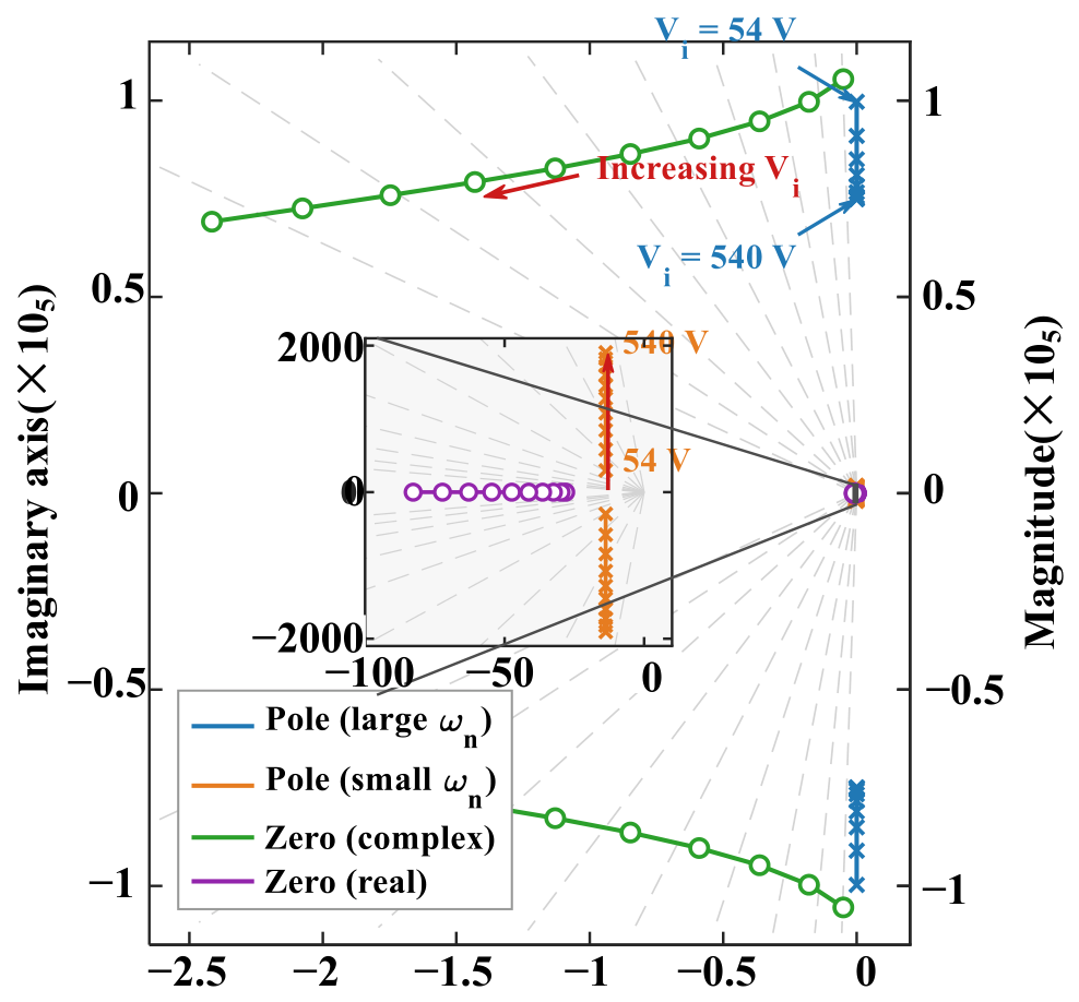
Figure 9, the pole–zero trajectories of
are obtained under different input-voltage conditions. With increasing voltage, the locations of the poles and zeros vary due to the change in the steady-state operating point. The low-frequency pole–zero pair dominates the dynamic performance of the current loop, whereas the high-frequency poles are mainly associated with parasitic parameters and switching-frequency-related effects.
According to the pole–zero distribution, the converter exhibits the worst dynamic performance under the maximum input-voltage condition (). Therefore, this operating point is selected as the design condition for the proportional–integral (PI) compensator to ensure sufficient stability margin over the entire input voltage range.
The inner current loop employs a PI compensator combined with a first-order low-pass filter to improve low-frequency tracking performance while suppressing high-frequency gain amplification. The corresponding continuous-time transfer function is expressed as
where
and
represent the proportional and integral coefficients of the current-loop compensator, respectively. According to the pole–zero distribution of
, the compensator zero is placed to compensate for the dominant low-frequency pole under the worst-case operating condition. Considering the 60 kHz switching frequency and the requirement for suppressing the 100 Hz double-line-frequency disturbance, the current-loop crossover frequency is selected in the kilohertz range. The parameters of the PI compensator are determined by evaluating the compensated open-loop transfer function
through Bode plot analysis. The proportional and integral gains are iteratively adjusted to achieve the desired crossover frequency while maintaining a sufficient phase margin for stable operation.
The optimized current-loop parameters are obtained as
and
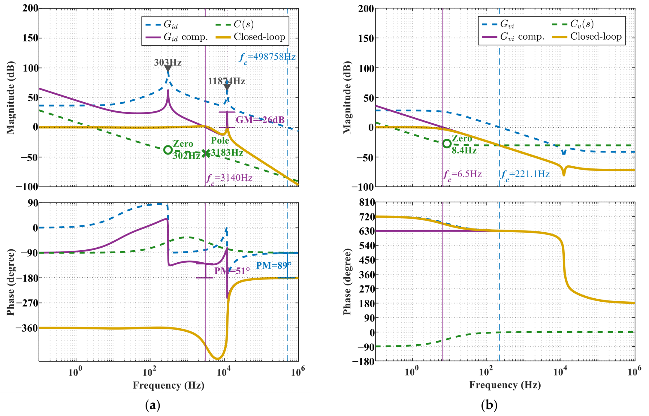
. As shown in
Figure 10a, the compensated current loop achieves an open-loop crossover frequency of approximately 3 kHz, with a phase margin of
, indicating satisfactory dynamic response and stability.
Considering the low-frequency energy storage characteristics of the output capacitor and the requirement for suppressing low-frequency output-voltage fluctuations, the voltage-loop crossover frequency is selected significantly lower than the current-loop bandwidth. Moreover, considering the half-line-cycle voltage fluctuation and digital implementation constraints, the voltage-loop crossover frequency is selected in the range of several hertz.
The integral coefficient is selected to improve the low-frequency regulation capability of the voltage loop. The designed parameters are selected as
and
. As shown in
Figure 10b, the compensated voltage loop achieves an open-loop crossover frequency of approximately 6.5 Hz with a sufficient phase margin.
The significantly lower bandwidth of the voltage loop compared with that of the current loop ensures effective dynamic decoupling between the two control loops and contributes to stable operation of the proposed dual-loop control system.
4.4. Adaptive CCM/DCM Mode Control Strategy
Due to the inherent operating characteristics of the proposed isolated three-phase interleaved SEPIC converter, the converter exhibits multiple conduction modes under wide input-voltage and load variations. During high-power operation, transitions between CCM and DCM inevitably occur, resulting in variations in current dynamics and potential distortion of the input current waveform if the transition process is not properly regulated.
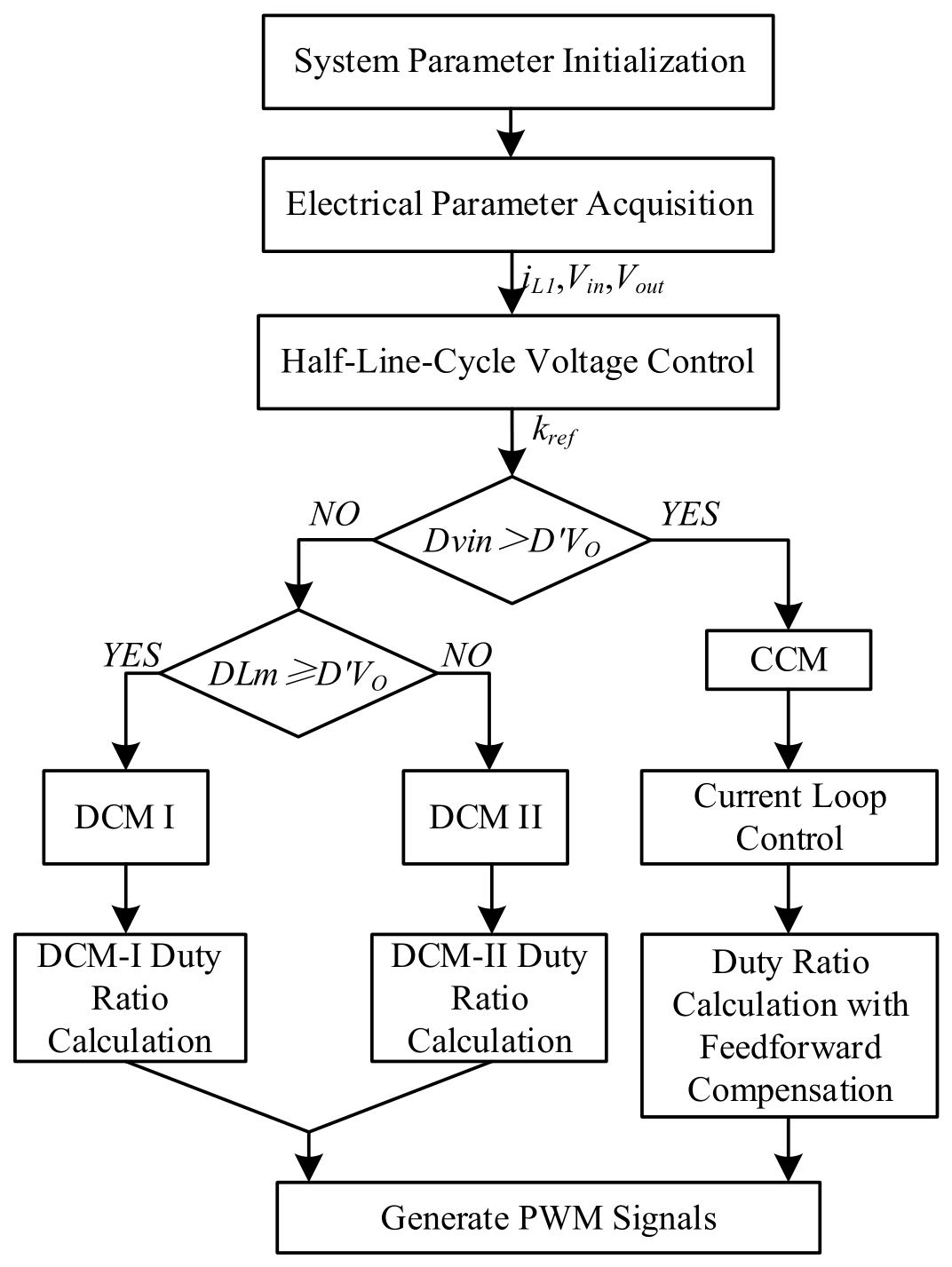
To address the dynamic mismatch associated with CCM/DCM transitions, an adaptive mode control strategy is proposed, as illustrated in
Figure 11. The proposed strategy integrates conduction-mode identification and mode-dependent control law selection, thereby enabling smooth transitions between different operating regions while maintaining stable current regulation.
The conduction mode is identified according to the boundary conditions derived in Equations (19) and (20). In practical operation, the equivalent inductance varies with the conduction mode and operating conditions. Therefore, instead of adopting a fixed inductance value for mode determination, the proposed method evaluates the instantaneous current evolution within each switching cycle to determine the corresponding conduction mode.
Specifically, when the inductor current remains continuous throughout the entire switching period, the converter is classified as operating in CCM. Otherwise, the DCM operation is further classified according to the current-overlap characteristics. In DCM-I operation, the inductor current reaches zero during the freewheeling interval, whereas in DCM-II operation, the inductor current becomes discontinuous within a shorter interval owing to insufficient energy transfer. This classification provides the basis for selecting the corresponding control strategy for each conduction mode.
When the converter operates in DCM, the duty ratio is determined according to the analytical relationships derived in Equations (24) and (25). In CCM operation, the voltage-loop output is employed to generate the current reference, and the inner current controller regulates the inductor current. The generated duty-ratio command is subsequently combined with the input-voltage feedforward component to improve dynamic performance.
To achieve smooth CCM/DCM transitions, an initial duty-ratio compensation mechanism is introduced during system initialization and mode conversion. When a transition from DCM to CCM occurs, a transition buffer interval is introduced, during which the initial duty ratio is maintained before the current-loop controller gradually takes over the regulation process. Similarly, the reverse transition from CCM to DCM is handled through the periodic symmetry of converter operation, avoiding abrupt variations caused by direct switching between different control laws.
Through the proposed adaptive mode control strategy, the converter achieves accurate conduction-mode identification and smooth mode transitions, ensuring stable operation over a wide input and load range.
5. Power Loss Analysis and Efficiency Evaluation
The power loss characteristics of the proposed isolated three-phase interleaved SEPIC converter are analyzed under the rated output power of 3 kW. Considering the symmetrical structure of the three-phase interleaved configuration, the loss evaluation is performed based on a single-phase conversion cell, and the total converter loss is obtained by considering the contribution of all parallel phases.
The total power loss consists of semiconductor losses, magnetic component losses, and auxiliary-circuit losses. The semiconductor losses mainly include the conduction and switching losses of the power switches and rectifier diodes. The magnetic losses are associated with the winding copper loss and core loss of the coupled inductors and the high-frequency transformer. In addition, the gate-drive circuit losses are included in the overall loss estimation.
The detailed loss models, including semiconductor conduction and switching losses, winding copper loss, and magnetic core loss, together with the corresponding device parameters, are provided in
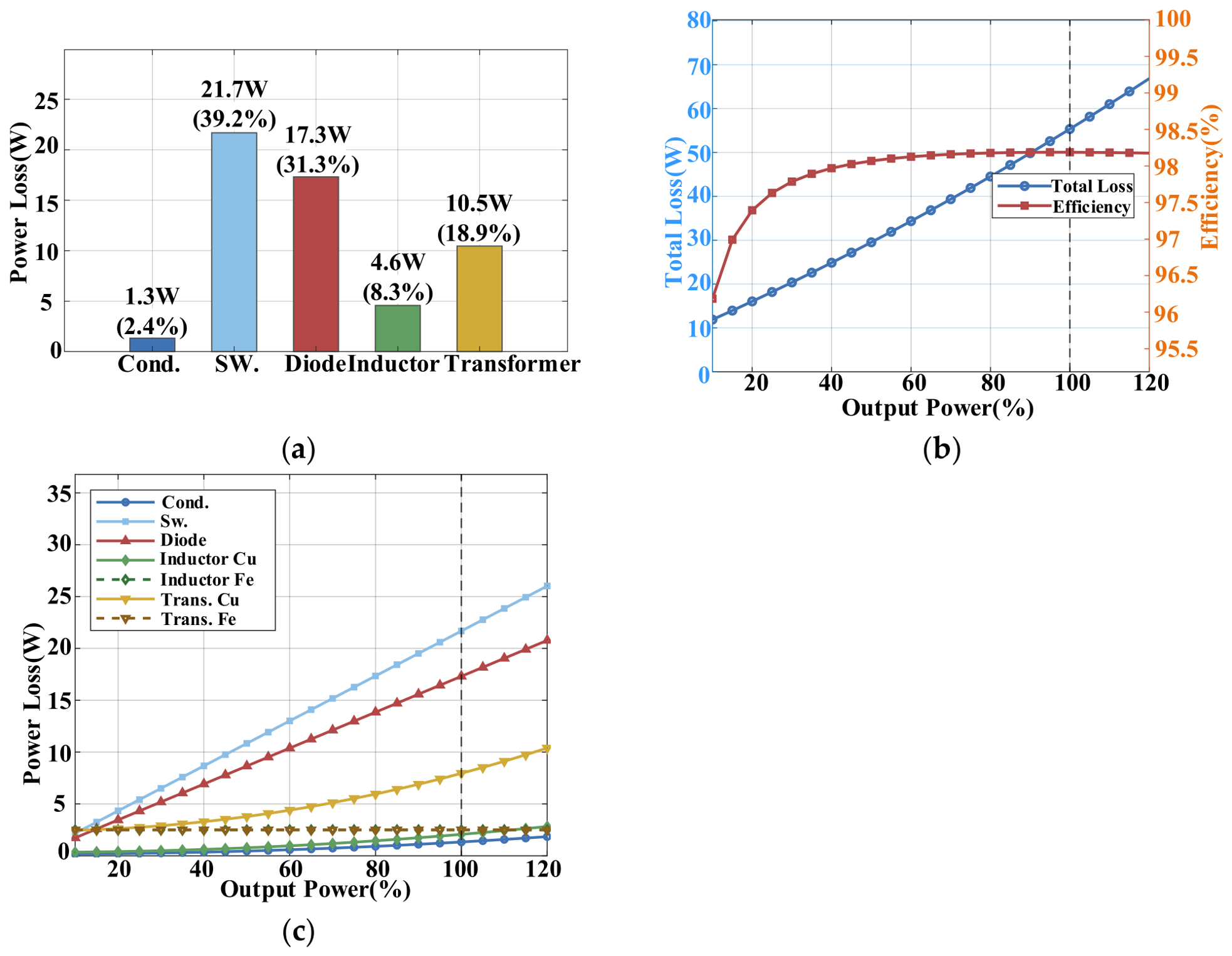
Appendix B. The calculated loss distribution and efficiency characteristics under different output power levels are presented in
Figure 12.
Figure 12a shows the loss distribution at the rated output power of 3 kW. The dominant losses originate from the semiconductor devices and magnetic components. The MOSFET switching loss accounts for a relatively large proportion due to the high switching frequency and turn-off current stress. The diode loss is also considerable because of the forward voltage drop during conduction, whereas the MOSFET conduction loss remains low owing to the low on-state resistance of the SiC devices.
Figure 12b presents the variation in different loss components with output power. The semiconductor and copper losses increase continuously with increasing load current, whereas the magnetic core losses remain almost unchanged because they are mainly affected by the voltage waveform and switching frequency. Therefore, fixed losses dominate under light-load conditions, whereas current-dependent losses become the major loss sources during high-power operation.
Figure 12c illustrates the total loss and efficiency characteristics from 10% to 120% rated power. The efficiency increases rapidly at low loads due to the reduced proportion of fixed losses and reaches its maximum near the rated operating point. When the output power exceeds the rated value, the efficiency gradually decreases because of increased conduction and copper losses. The calculated efficiency at a 3 kW output power is approximately 98%, which agrees well with the experimental results.
6. Simulation and Experimental Verification
6.1. Simulation Verification
To verify the theoretical analysis presented in the previous sections, a detailed simulation model of the proposed three-phase modular parallel isolated SEPIC converter was developed in MATLAB/Simulink R2020a. The simulation parameters were selected according to the hardware specifications listed in
Table 1. Steady-state operation, conduction-mode transition, input current quality, and dynamic performance under load disturbances were comprehensively evaluated to validate both the proposed converter topology and the designed dual-loop control strategy.
The simulation results presented in the following subsections are organized according to the theoretical analysis in
Section 3,
Section 4 and
Section 5. Particular attention is paid to the steady-state characteristics, current quality, transient response, and CCM/DCM transition behavior. The consistency between the theoretical predictions and the simulation results demonstrates the validity of the proposed analytical model and control method.
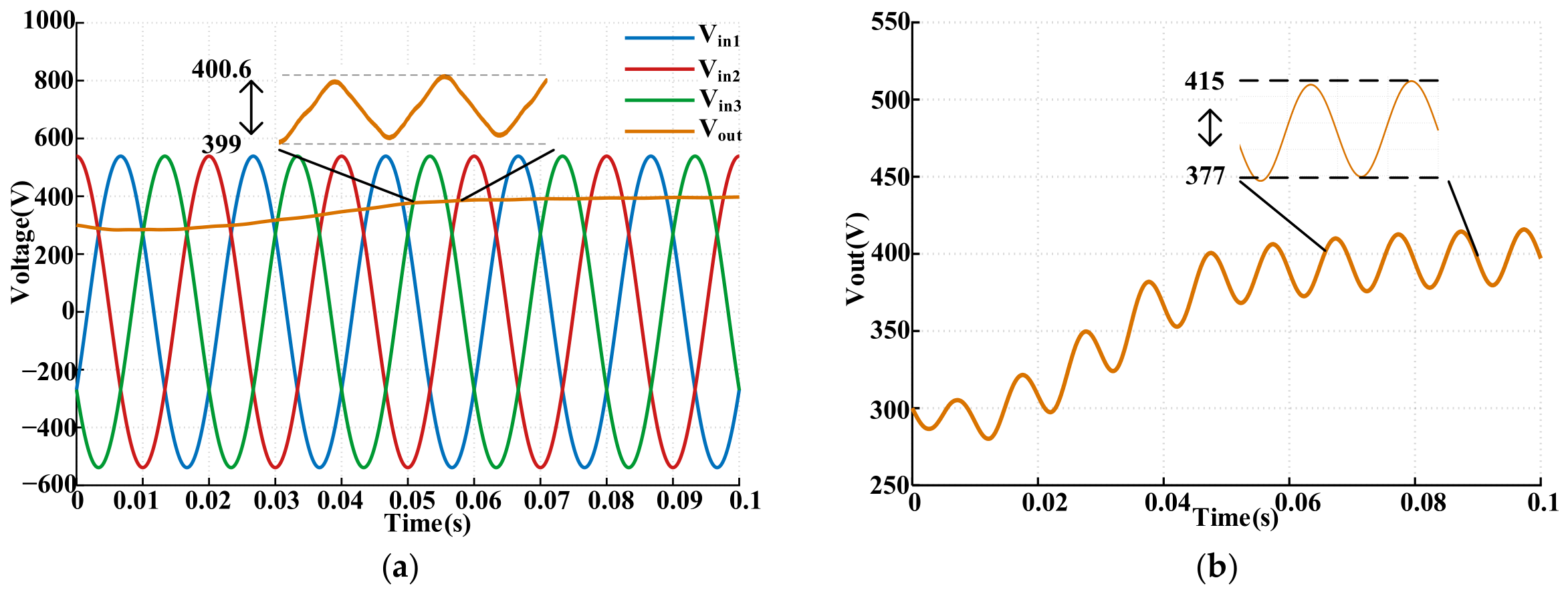
Figure 13a presents the simulated input and output voltage waveforms of the proposed three-phase parallel isolated SEPIC converter. The output voltage is regulated at approximately 400 V under the rated condition, with a peak-to-peak voltage ripple of about 1.6 V, indicating good voltage regulation performance.
Figure 13b shows the output voltage waveform of the conventional single-phase SEPIC converter under the same condition. Compared with the single-phase configuration, the proposed three-phase parallel structure effectively reduces the output voltage ripple. This improvement is mainly attributed to the 120° phase displacement of the three-phase input voltages, which produces ripple components with different phase angles in each phase and reduces the resultant output voltage ripple after superposition.
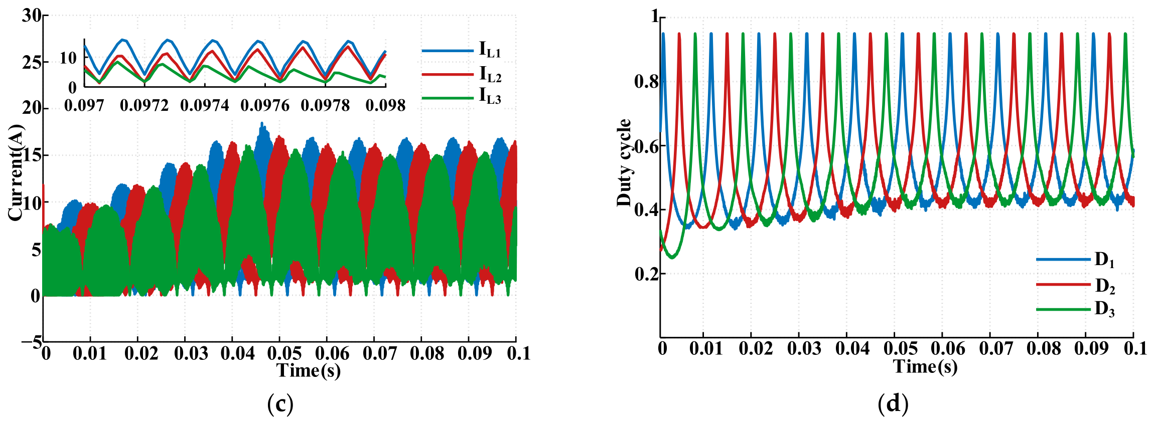
Figure 13c illustrates the inductor current waveforms of the three phases. The three phase currents exhibit a 120° phase difference due to the characteristics of the three-phase input source, and similar current amplitudes are observed among the parallel phases. The converter operates in DCM at low current levels and transitions to CCM under higher current conditions. The detailed CCM/DCM transition process is further analyzed in
Figure 14.
Figure 13d depicts the duty-cycle waveforms of the three parallel SEPIC cells. Owing to the 120° phase displacement of the three-phase input voltages, the duty ratios of the three phases vary periodically with the line cycle while maintaining identical modulation characteristics. The duty cycles are automatically adjusted by the proposed dual-loop controller according to the instantaneous operating conditions and remain within the allowable modulation range throughout the entire line cycle. Moreover, the close agreement among the three duty-cycle profiles demonstrates the balanced operation of the parallel conversion cells and ensures consistent current sharing, which is in accordance with the inductor current characteristics shown in
Figure 13c.
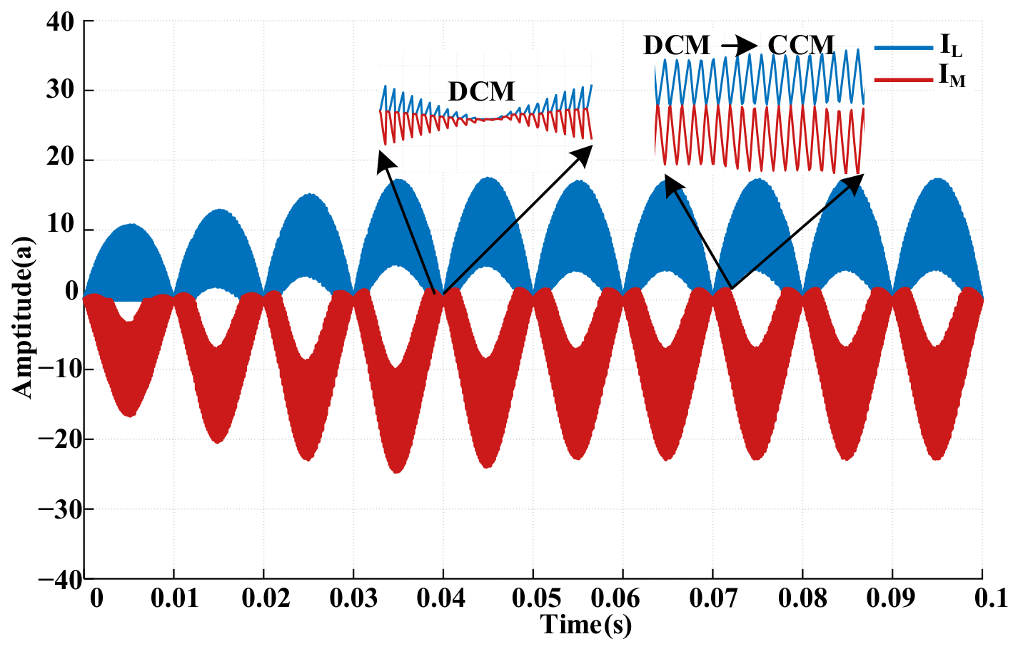
Figure 14 presents the simulated current waveforms of the input inductor
and magnetizing inductance
for one phase of the proposed converter. The enlarged waveforms clearly demonstrate the typical characteristics of both DCM and CCM operations, which agree well with the theoretical analysis. Furthermore, the transition between DCM and CCM is smooth under the proposed conduction-mode switching strategy, without significant current distortion. The results verify the effectiveness of the proposed mode transition strategy and ensure stable operation over a wide load range.
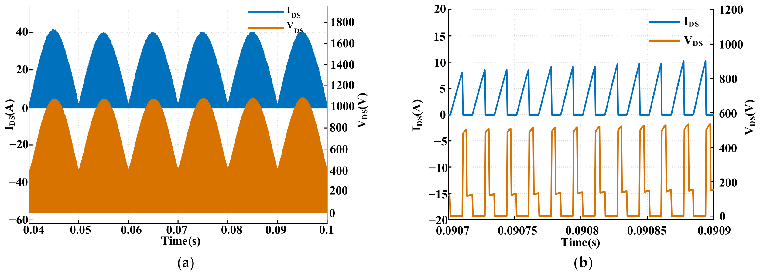
Figure 15 presents the simulated voltage and current stresses of the main switch under rated operating conditions. As shown in
Figure 15a, the drain-source voltage
exhibits a high voltage stress due to the superposition of the output voltage and the input-side voltage component. When the input voltage reaches 540 V, the theoretical voltage stress of the switch exceeds 940 V. Moreover, considering the voltage overshoot caused by parasitic parameters during the switching transition, the actual voltage stress is further increased.
Meanwhile, the switch current presents a triangular waveform, resulting in a relatively high turn-off current. The simultaneous high voltage and current during the turn-off process lead to considerable switching losses, which become one of the major loss contributors of the proposed converter. The enlarged waveform in
Figure 15b provides a detailed view of the switching transient, which agrees well with the theoretical analysis.
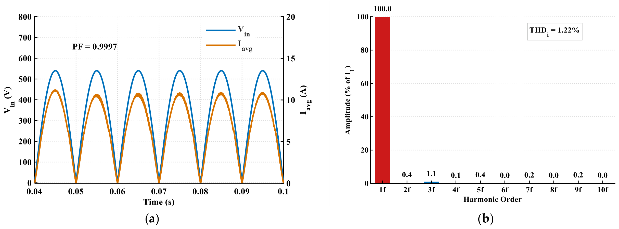
Figure 16 presents the simulated input power quality characteristics of the proposed converter. As shown in
Figure 16a, the input power factor reaches 0.9997 under the rated operating condition, indicating that the proposed converter achieves nearly unity power factor operation.
Figure 16b shows the harmonic spectrum of the input current. The total harmonic distortion (THD) is only 1.22%, and the third-order harmonic component is limited to approximately 1%, demonstrating the excellent input current quality and effective harmonic suppression capability. Therefore, the proposed three-phase parallel isolated SEPIC converter exhibits satisfactory steady-state performance in terms of voltage regulation, power factor correction, and harmonic distortion reduction.
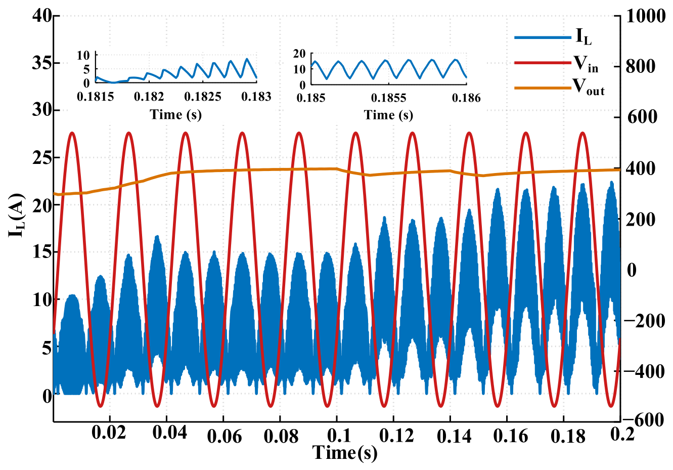
Figure 17 presents the simulated dynamic response of the proposed converter under load step variations. The load transients are introduced at 0.1 s and 0.14 s, respectively. As observed from the waveform, the output voltage experiences noticeable deviations during the load changes and requires approximately 0.04 s to recover after the first disturbance. During the second load variation, the output voltage returns to the rated value after about 0.06 s.
The relatively slow voltage recovery is mainly attributed to the adopted voltage-loop control strategy, where the voltage regulation process is updated within a half-line-cycle period. Therefore, a certain delay exists between the occurrence of the load disturbance and the corresponding control action, resulting in a limited transient response speed.
Considering the characteristics of the proposed converter, the relatively slow dynamic response makes it more suitable for applications with slowly varying loads, such as battery energy storage systems. For applications requiring fast load transient response, an additional compensation unit, such as a parallel supercapacitor, can be introduced. Furthermore, by replacing the outer voltage-loop control with a current-loop control strategy, the converter can be extended to constant-current charging applications.
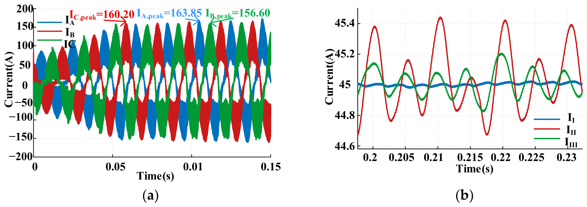
To further evaluate the scalability of the proposed modular architecture, an additional 54 kW three-module simulation model was established based on the identical SEPIC conversion cell and control strategy adopted in the experimentally verified 18 kW prototype. The objective of this simulation is to investigate whether the proposed parallel architecture and current-sharing control strategy can be extended to a higher-power configuration without modifying the fundamental converter structure.
Figure 18a presents the three-phase input currents under the 54 kW operating condition. The peak values of the three-phase currents are
A,
A, and
A, respectively. The three input phase currents maintain a balanced distribution, demonstrating that the proposed architecture can preserve the three-phase power processing capability after increasing the number of parallel modules.
Furthermore, the output currents of the three parallel modules are shown in
Figure 18. The average output currents of Module I, Module II, and Module III are approximately 45.00 A, 45.07 A, and 44.99 A, respectively. Since the three modules are connected in parallel and share the same output voltage, the output current distribution directly represents the power-sharing performance among the modules. The maximum current deviation among the three modules is approximately 0.18% based on the average current values, indicating excellent current-sharing capability under the three-module configuration.
These simulation results further demonstrate the scalability of the proposed modular architecture. The experimentally verified 18 kW dual-module prototype confirms the feasibility of the modular operation and current-sharing strategy, while the 54 kW three-module simulation provides additional verification of the potential for further power expansion.
6.2. Experimental Prototype and Test Setup
To further validate the theoretical analysis and simulation results, an 18 kW experimental prototype of the proposed three-phase parallel isolated SEPIC converter is developed and experimentally tested. The prototype adopts a modular power board structure, where each power board consists of two identical power modules (Power Module I and Power Module II) and provides an 18 kW power conversion capability. The main circuit parameters and design specifications are consistent with those listed in
Table 1. During the experimental tests, a Tektronix MSO54 mixed-signal oscilloscope (manufactured by Tektronix, Inc., Beaverton, OR, USA) is employed to capture the voltage and current waveforms of the converter, ensuring reliable acquisition of the experimental signals.
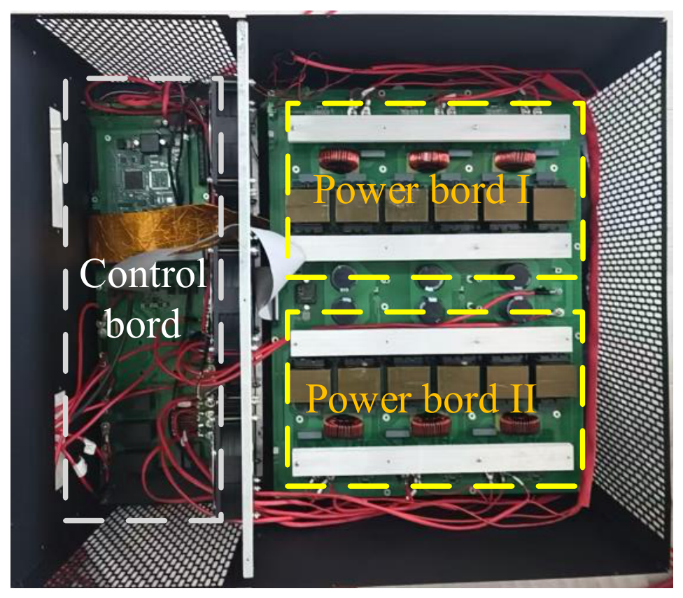
The experimental platform is shown in
Figure 19. A programmable AC source is employed to provide the three-phase input voltage. A DC resistive load is utilized at the output side for performance evaluation. The developed 18 kW prototype is presented in
Figure 19, which consists of a control board and a power board. Benefiting from the modular design, the proposed converter can be further expanded by connecting multiple power boards in parallel. Benefiting from the modular design, the proposed converter can be further expanded by connecting multiple power boards in parallel. The identical structure of each power board provides the possibility of extending the output power toward higher power levels, such as 54 kW, by paralleling multiple modules. The 18 kW prototype experimentally verifies the feasibility of the modular architecture and current-sharing capability.
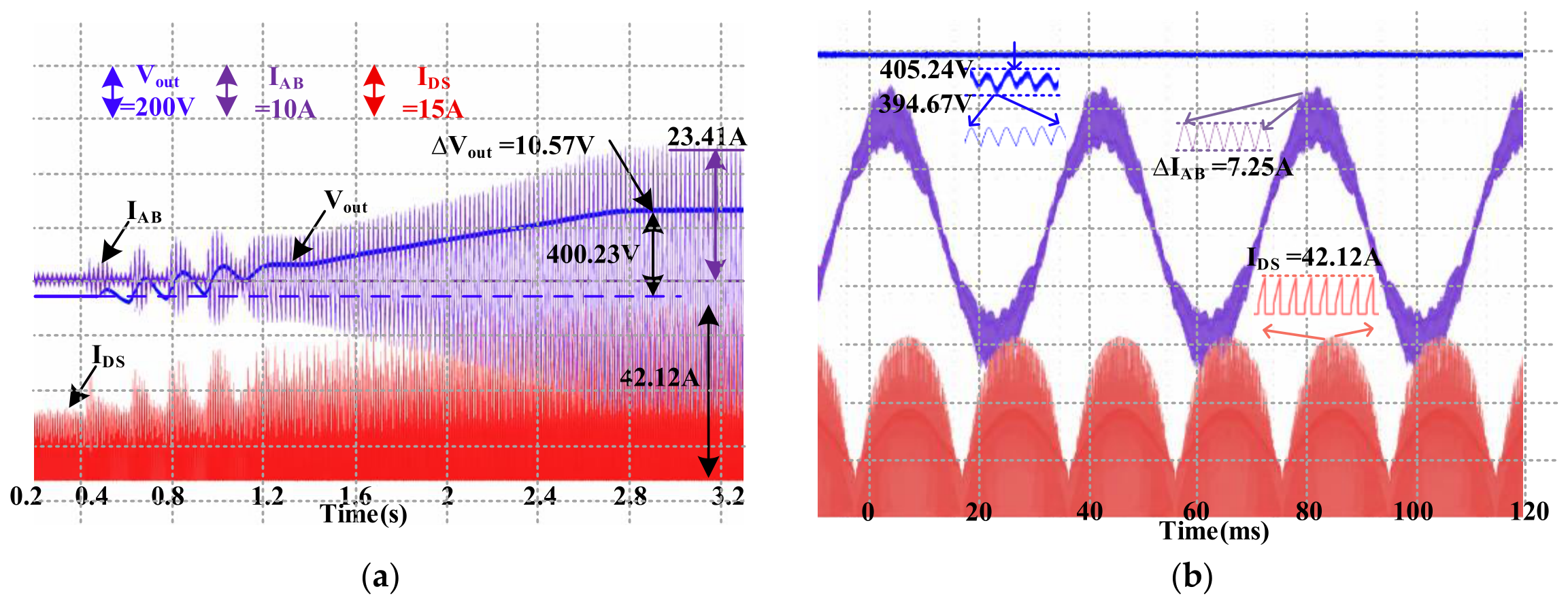
Figure 20 presents the startup transient response of the proposed power unit using the soft-start strategy. The startup time is approximately 2.4 s, during which the soft-start control effectively suppresses the excessive inrush voltage and prevents output voltage overshoot. The output voltage
is regulated at 400.23 V with a voltage ripple of approximately 10.57 V, fluctuating within the range of 395–405 V. The measured current waveform represents the input phase current. For a single 3 kW power unit, the peak input current reaches approximately 23.41 A. As the output power increases, the drain current
gradually rises, and the turn-off current spike reaches approximately 42.12 A due to the increased switching stress.
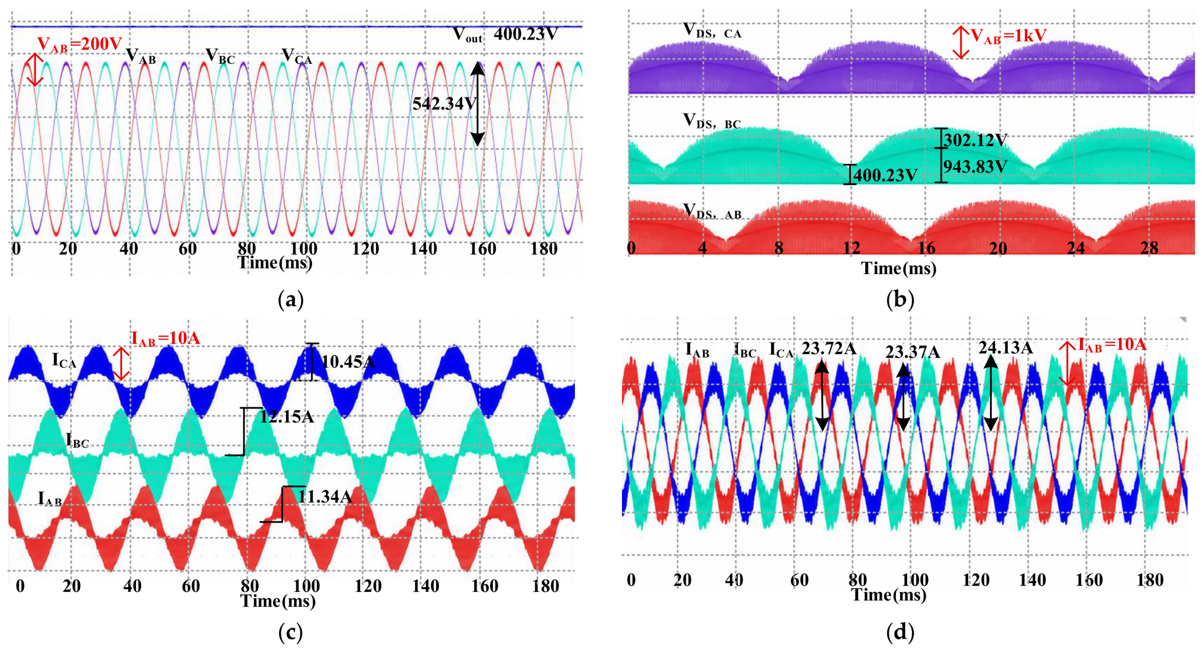
Figure 21 presents the experimental steady-state waveforms of the proposed converter under different load conditions. (a) shows the full-load steady-state waveforms, including the input phase voltage and the output voltage. The peak input phase voltage is approximately 542.34 V, while the output voltage is stably regulated at 400.23 V; (b) shows the drain-to-source voltage
of the SiC MOSFET. The measured results indicate that the theoretical voltage stress across the device satisfies Equation (15). However, owing to the switching transients and parasitic parameters of the practical SiC MOSFET circuit, voltage overshoot occurs during switching, resulting in an actual peak
of approximately 1240 V. (c) presents the converter waveforms under light-load operation. It can be observed that the converter operates in discontinuous conduction mode (DCM), with a peak current envelope value of approximately 10.45 A. (d) shows the input phase-current waveform under full-load operation. The peak phase current is approximately 23.37 A. The current waveform remains stable and well regulated, demonstrating the satisfactory steady-state performance of the proposed system.
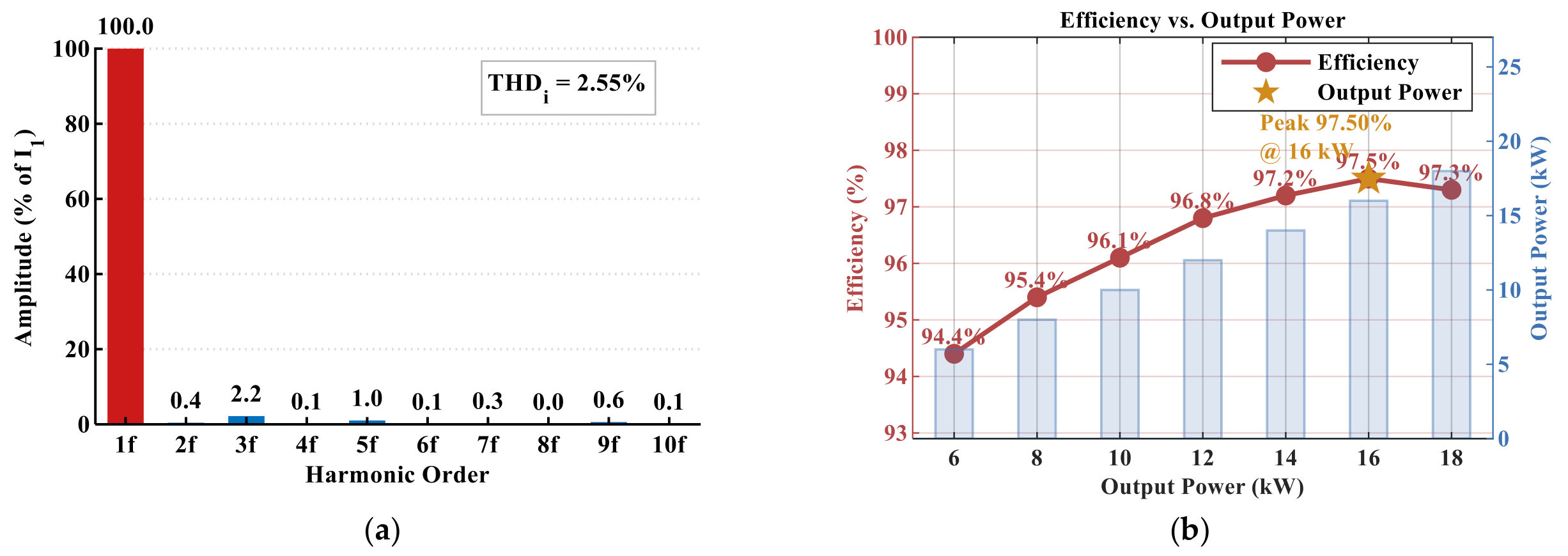
The measured waveform data were exported and processed to evaluate the input power quality. The calculated power factor (PF) is 0.991, while the total harmonic distortion (THD) of the input current is 2.55%. As shown in
Figure 22a, the harmonic components are effectively suppressed, indicating good input-current quality and satisfactory power factor correction performance.
Figure 22b presents the measured efficiency as a function of the output power. The conversion efficiency gradually increases with increasing output power and reaches a maximum value of 97.5%. At the rated load, the efficiency is approximately 97.3%. The slight reduction in efficiency near full-load operation is mainly attributed to the increased device temperature at high power levels, which leads to higher conduction and switching losses.
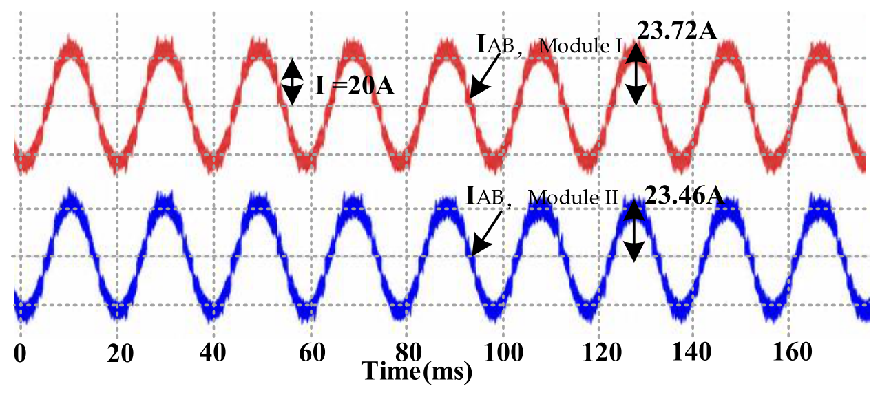
Furthermore, the current-sharing performance of the parallel power modules is experimentally investigated under full-load operation. As shown in
Figure 23, the AB-phase currents of Power Module I and Power Module II exhibit highly consistent waveforms, indicating that the power distribution between the parallel modules is well balanced. The measured peak currents of Power Module I and Power Module II are 23.72 A and 23.46 A, respectively, resulting in a current difference of only 1.10%. Therefore, the effectiveness of the proposed parallel structure and current-sharing capability is experimentally verified.
Overall, the five experimental waveforms verify the stable operation and satisfactory performance of the proposed converter under different operating conditions. The soft-start strategy effectively limits the startup transient and enables the output voltage to rise smoothly to its reference value without significant overshoot. Under steady-state operation, the output voltage remains well regulated, while the input phase voltage and current exhibit stable waveforms. The measured drain-to-source voltage confirms the expected voltage–stress relationship, although additional voltage overshoot is introduced by switching transients and circuit parasitic parameters. Under light-load conditions, the converter operates in discontinuous conduction mode, whereas stable continuous power transfer is achieved at full load. These results demonstrate that the proposed system provides good startup behavior, output-voltage regulation, current control, and steady-state performance over a wide load range.
To further demonstrate the advantages of the proposed converter, a comprehensive performance comparison with other reported EV charging converters is presented in
Table 2. Compared with existing EV-charging converters, the proposed topology achieves competitive harmonic performance while maintaining a relatively simple structure and high-power conversion capability.
7. Discussion
The proposed three-phase modular parallel isolated SEPIC converter provides a compact solution for high-power EV fast-charging applications. Compared with conventional cascaded AC–DC and DC–DC converters, the proposed quasi-single-stage architecture integrates power conversion, voltage regulation, and galvanic isolation functions into a simplified structure. By reducing the number of power conversion stages, magnetic components, and passive elements, the proposed converter achieves a favorable trade-off among efficiency, power density, and system cost. Furthermore, the modular parallel configuration enables flexible power expansion while maintaining the basic electrical characteristics of individual conversion units.
Although the proposed converter achieves high efficiency and excellent input power quality, the concentrated energy processing within the SEPIC conversion cell results in increased electrical stress on key components. Compared with multi-stage converters, the voltage and current stresses of semiconductor devices and magnetic components require additional consideration under high-power operation. Therefore, further optimization of semiconductor selection, magnetic design, and soft-switching techniques is necessary to improve the scalability and reliability of the converter for higher power levels.
It should be noted that the proposed topology employs an uncontrolled diode bridge at the input side and should, therefore, be considered a quasi-single-stage converter rather than a fully active single-stage solution. The diode bridge simplifies the circuit structure, reduces control complexity, and lowers system cost, which is beneficial for practical EV-charging applications. However, the additional conduction losses introduced by the rectifier limit further improvements in efficiency and power density. Future work will investigate bridgeless or active rectification techniques to enhance converter performance.
The developed control strategy is mainly designed for EV battery-charging applications, where the output characteristics are relatively stable. For applications involving large and rapid load variations, the dynamic response capability may require further improvement. Advanced control methods, such as adaptive control and predictive control, will be explored to enhance transient performance under more complex operating conditions.
Overall, the proposed quasi-single-stage converter demonstrates the feasibility of achieving high efficiency, modular scalability, and cost-effective implementation for EV fast-charging systems. The identified limitations also provide clear directions for future improvements in topology optimization, device stress reduction, and control strategy development.