1. Introduction
In recent years, the rapid advancement of Internet of Things (IoT) technology has driven the widespread deployment of low-power sensor nodes in applications such as environmental monitoring, intelligent manufacturing, and smart cities. However, these nodes are generally powered by batteries, which suffer from limited lifetime, high maintenance cost, and inconvenient replacement, thereby severely restricting the long-term stable operation of the system. In this context, harvesting ambient Radio Frequency (RF) energy for wireless power supply has emerged as a highly promising solution [
1]. Structurally, a basic RF energy harvesting system comprises an antenna, an impedance matching network, a rectifier circuit, and a load. Among these components, the rectifier serves as the core entity responsible for converting RF energy into usable DC power, and its performance directly determines the overall energy conversion efficiency and output capability of the system [
2].
Transcending the traditional boundaries of isolated circuit design, recent comprehensive review articles emphasize that RF energy harvesting must be investigated within the broader framework of complete battery-free wireless systems rather than being treated as an isolated rectifier problem [
3]. These systematic studies demonstrate that practical RF energy harvesting deployments encompass a holistic system-level ecosystem involving ambient or dedicated RF sources, receiving antennas, impedance matching networks, rectifier circuits, power management modules, energy storage units, and ultralow-power sensing or communication loads [
4]. Current research paradigms heavily focus on rectenna co-design, RF-to-DC conversion efficiency enhancement, multiband energy capturing, IoT integration, and battery-free autonomous platforms. Nevertheless, persistent challenges remain, including low ambient RF power density, inherent energy intermittency, strict miniaturization constraints, and the urgent demand for efficient multiband or adaptive harvesting topologies.
Within this diverse architectural landscape, the 2.45 GHz Industrial, Scientific, Medical (ISM) band exhibits a relatively high energy density due to the ubiquitous deployment of wireless communication devices such as Wi-Fi and Bluetooth, making it a primary target for energy harvesting [
5]. However, practical RF energy harvesting systems are strictly required to strike a fine balance among multiple conflicting performance metrics, including compact size, multiband operation, load-driving capability, and DC output voltage. Consequently, developing a compact rectifier that combines multiband energy harvesting potential with enhanced DC output capability remains important for RF-powered IoT devices and wireless sensing applications [
6]. In this work, the proposed rectifier is primarily positioned as a compact RF rectification front end for dedicated RF excitation, near-field wireless powering, or scenarios with relatively high incident RF power density. Its multiband response also indicates potential applicability to ambient RF energy harvesting; however, under weak and intermittent ambient RF conditions, practical operation would generally require integration with energy storage elements or power management circuits.
At present, extensive research has been conducted worldwide on RF rectifier circuits. In the field of high-efficiency rectifier design, numerous studies have achieved significant progress. Liu et al. proposed a compact dual-band impedance matching network composed of a three-section single-stage T-shaped transmission line structure. The designed 0.915 and 2.45 GHz rectifier, optimized for a 2500 Ω load, achieved conversion efficiencies of 81.7% and 73.1% at 12 dBm input power, respectively, providing an effective solution for powering passive IoT nodes. However, its load-driving capability still requires further improvement [
7]. Mansour et al. designed a compact dual-band RF rectifier operating at 920 MHz and 2.4 GHz using a T-shaped matching network and SMS7630 Schottky diode. The rectifier maintained conversion efficiencies above 45% in both bands, with a peak efficiency of 70% at 2.4 GHz. Under 5 dBm input power and an optimal 4.7 kΩ load, the circuit generated a DC output voltage of 2.66 V, making it suitable for ambient RF energy harvesting [
8]. Zhang et al. proposed a broadband microwave rectifier combining a voltage-doubling structure with a broadband impedance matching network to achieve high-efficiency rectification over 600 MHz–1.6 GHz. Experimental results demonstrated efficiencies above 60% under 16–30 dBm input power, with a peak efficiency of 84%, verifying the importance of broadband matching structures in improving RF-DC conversion efficiency [
9]. Xiao et al. proposed a dual-band Class-F rectifier operating at 2.45 GHz and 5.8 GHz. By employing a dual-band harmonic termination network to control second- and third-order harmonics, the rectifier achieved peak RF-DC efficiencies of 74.9% and 61.9%, with corresponding DC output voltages of 2.74 V and 3.94 V, respectively, demonstrating favorable dual-band high-efficiency characteristics [
10]. However, such high-efficiency designs usually rely heavily on specific impedance matching conditions or complex harmonic suppression circuits, and their optimal performance is often obtained under light-load (high-impedance) conditions. When applied to practical heavy-load scenarios, the output voltage capability tends to decrease rapidly, making it difficult to directly drive logic-level devices.
In terms of output voltage enhancement, researchers mainly improve the DC output capability through voltage multiplier topologies and multistage rectifier structures. T. Sathiyapriya et al. designed a five-stage voltage-doubling rectifier based on the HSMS2820 Schottky diode for an 875 MHz RF energy harvesting system. Without requiring an additional DC boost module, the circuit achieved a DC output power of 64 mW and a conversion efficiency of 24% at 0 dBm input power, enabling direct powering of low-power sensors while effectively replacing batteries and reducing cost [
11]. Muhammad et al. proposed a compact single-stage voltage-doubling rectifier operating at 900 MHz using an HSMS2850 Schottky diode and an L-shaped matching network. Under a 2 kΩ load and 14 dBm input power, the rectifier achieved a DC output voltage of 3.1 V with a conversion efficiency of 50.2%, making it suitable for ambient RF energy harvesting in low-power IoT devices [
12]. Adam et al. proposed a cascaded voltage-multiplying rectifier operating in the 2.4 GHz ISM band. By employing a six-stage Dickson voltage multiplier structure, the rectifier achieved an output voltage of 3.4 V under 0 dBm input power, demonstrating its suitability for RF energy harvesting in low-power IoT applications [
13]. Benkalfate et al. proposed a switchable dual-architecture RF energy harvesting system for wireless sensor networks covering 1.8, 2.1, and 2.66 GHz bands. Through MOSFET switching, the system automatically selected the optimal rectifier structure under different input power levels. A maximum output voltage of 3.15 V was obtained under a 2 kΩ load, verifying the effectiveness of multistage voltage multiplier structures in enhancing output capability [
14]. However, most existing voltage multiplier circuits either operate at relatively low frequencies (such as 900 MHz) or require many multiplication stages to achieve high output voltage at 2.4 GHz. This increases circuit size, introduces additional parasitic losses, and makes it difficult to simultaneously achieve high-voltage output and compact design.
In terms of wideband and multi-band energy harvesting, multi-frequency rectification technology has garnered significant attention as ambient RF sources increasingly exhibit multi-frequency distribution characteristics. Joseph et al. proposed a compact wideband rectifier based on a three-stage transmission line impedance matching network. By synergistically employing linearly tapered microstrip lines, short-circuited stubs, and open-circuited stubs, wideband impedance matching and low-loss characteristics were achieved. At an input power of 5 dBm, the rectifier realized an operating frequency band of 1.12–2.43 GHz, corresponding to a fractional bandwidth of 74%, with a power conversion efficiency (PCE) exceeding 50% across the entire band [
15]. Lawan et al. presented an RF rectifier circuit operating in the 2.45 GHz band that utilizes a voltage-controlled MOSFET switch to maintain high conversion efficiency over a wide range of input powers. Combined with an L-type matching network and a DC-blocking capacitor, the efficiency remained above 50% within an input power range of 3–23.8 dBm, reaching a peak efficiency of 73% at 16.6 dBm, thereby effectively breaking through the efficiency bottlenecks of traditional topologies in high-frequency, wide-power scenarios [
16]. Pham et al. proposed a tri-band rectenna system based on composite right/left-handed (CRLH) technology; its accompanying high-sensitivity rectifier achieved peak conversion efficiencies of 80%, 46%, and 42% at 940 MHz, 1.95 GHz, and 2.44 GHz, respectively, under an input power of 0 dBm, demonstrating significant gains from multi-band collaborative rectification [
17]. Khansalee et al. introduced a dual-band RF energy harvesting rectifier operating at 2.1 GHz and 2.45 GHz, utilizing an HSMS-285C Schottky diode and a Greinacher voltage doubler structure; at a 10 dBm input, it delivered an output of 1.9 V with 24% efficiency in the 2.1 GHz band, and 1.7 V with 18% efficiency in the 2.45 GHz band, making it suitable for powering low-power passive sensors [
18]. Current wideband and multi-band rectification technologies effectively enhance the harvesting efficiency of complex ambient energy through methods such as tapered transmission lines, active switch control, and composite materials. However, while pursuing multi-frequency characteristics, existing studies often struggle to balance compact physical size with high voltage driving capability. In particular, when faced with the requirement of directly driving a 5 V logic level, their output performance remains insufficient.
In summary, although existing research on radiofrequency rectifier circuits has yielded fruitful results in improving conversion efficiency, expanding operating bandwidth, and enabling multi-frequency synergy, several critical trade-off challenges persist in practical engineering applications. High-efficiency designs typically rely on harmonic suppression techniques or high-impedance narrowband matching conditions tailored to specific frequency bands, making it inherently difficult to maintain a compact footprint while simultaneously ensuring robust and stable voltage output performance under heavy loads. Concurrently, although multi-stage voltage doubler structures can effectively boost the output voltage, the accompanying amplification of parasitic losses and increased circuit complexity strictly limit their deployment in highly miniaturized systems. Furthermore, while multi-band and wideband rectifying topologies successfully expand the harvesting range of ambient energy, they generally require complex matching networks, which inevitably introduce additional insertion losses and degrade the energy conversion efficiency at individual frequency points. Therefore, how to implement a compact RF rectifier that simultaneously delivers a stable 5 V direct-drive output under heavy loads and supports multi-frequency energy capturing remains a critical technical bottleneck for self-powered Internet of Things nodes.
From the perspective of impedance matching, conventional RF rectifiers commonly employ lumped-element L-, ∏-, or T-type matching networks, single-stub or double-stub microstrip matching structures, stepped-impedance transmission lines, tapered transmission lines, and harmonic termination networks. To further optimize performance, researchers have widely utilized parametric sweeps, response-surface methodology, genetic algorithms, and particle swarm optimization to tune the geometrical or electrical parameters of matching networks. Although these traditional multi-variable impedance matching approaches are effective in reducing reflection loss and enhancing the RF-to-DC conversion efficiency at target operating frequencies, they primarily focus on macroscopically obtaining a desired equivalent input impedance at the source port. Consequently, the continuous distributed impedance transformation process along the physical microstrip transmission path, as well as its complex dynamic coupling behavior with the non-linear rectification characteristics of the diode, typically lacks a systematic and explicit analysis.
To address these critical challenges, this paper presents a compact and efficient radiofrequency rectifier design method based on the SMS7621 Schottky diode, with its core contribution being an 11-segment microstrip distributed-parameter collaborative optimization strategy. Unlike conventional approaches that achieve impedance matching merely by tuning a few discrete geometric or lumped parameters, this strategy divides the entire microstrip matching path into eleven electrically interconnected, independent transmission line segments, and comprehensively accounts for their collaborative effects on the overall impedance matching performance as well as the compensation of the diode’s nonlinear input impedance and parasitic effects during the co-optimization process. Within this framework, each transmission line segment is no longer treated as an isolated optimization variable; instead, it is modeled and analyzed as an integral part of a unified, distributed parameter-nonlinear rectification network for global co-design and optimization. By integrating sensitivity analysis with genetic-algorithm-assisted optimization, the critical transmission line parameters are collaboratively optimized, thereby improving the nonlinear input impedance matching characteristics of the SMS7621 diode and effectively compensating for its package parasitics to achieve an optimal impedance matching effect. Therefore, the contribution of this strategy does not lie in the use of transmission-line length tuning itself, but in the adoption of a segment-level sensitivity-guided optimization framework that integrates the distributed microstrip layout, nonlinear rectifier impedance variation, and multiband RF-to-DC response within a compact rectifier design.
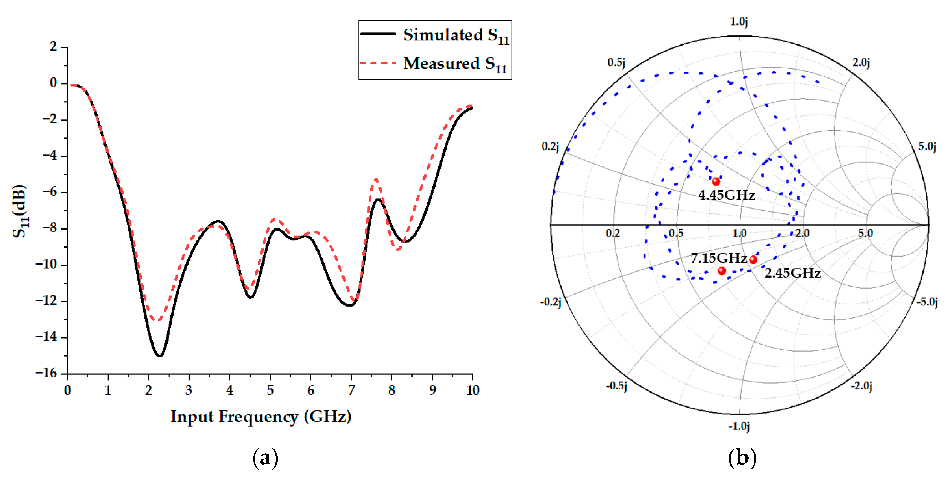
Through this distributed-parameter collaborative optimization strategy, precise impedance matching is successfully achieved within a single-layer compact structure of only 3.48 cm × 1.98 cm. Furthermore, the optimized configuration naturally supports three resonant modes at 2.45 GHz, 4.45 GHz, and 7.15 GHz, thereby endowing the rectifier with multi-band RF energy harvesting capabilities. Experimental results demonstrate that the proposed rectifier circuit exhibits excellent RF-to-DC conversion performance in the vicinity of the 2.45 GHz band, achieving a maximum measured DC output voltage of 5.42 V under an input power of 25 dBm and a 300 Ω heavy load condition. Benefiting from this output capability, the rectifier shows the potential to support low-power microcontrollers and sensor-node loads without requiring an additional DC–DC boost converter under controlled RF powering conditions, providing a compact front-end option for integrated RF-powered wireless sensing systems.
2. Circuit Design and Modeling
2.1. Rectifier Circuit Topology
In an RF energy harvesting system, the rectification circuit serves as a critical module for converting high-frequency AC signals into DC energy [
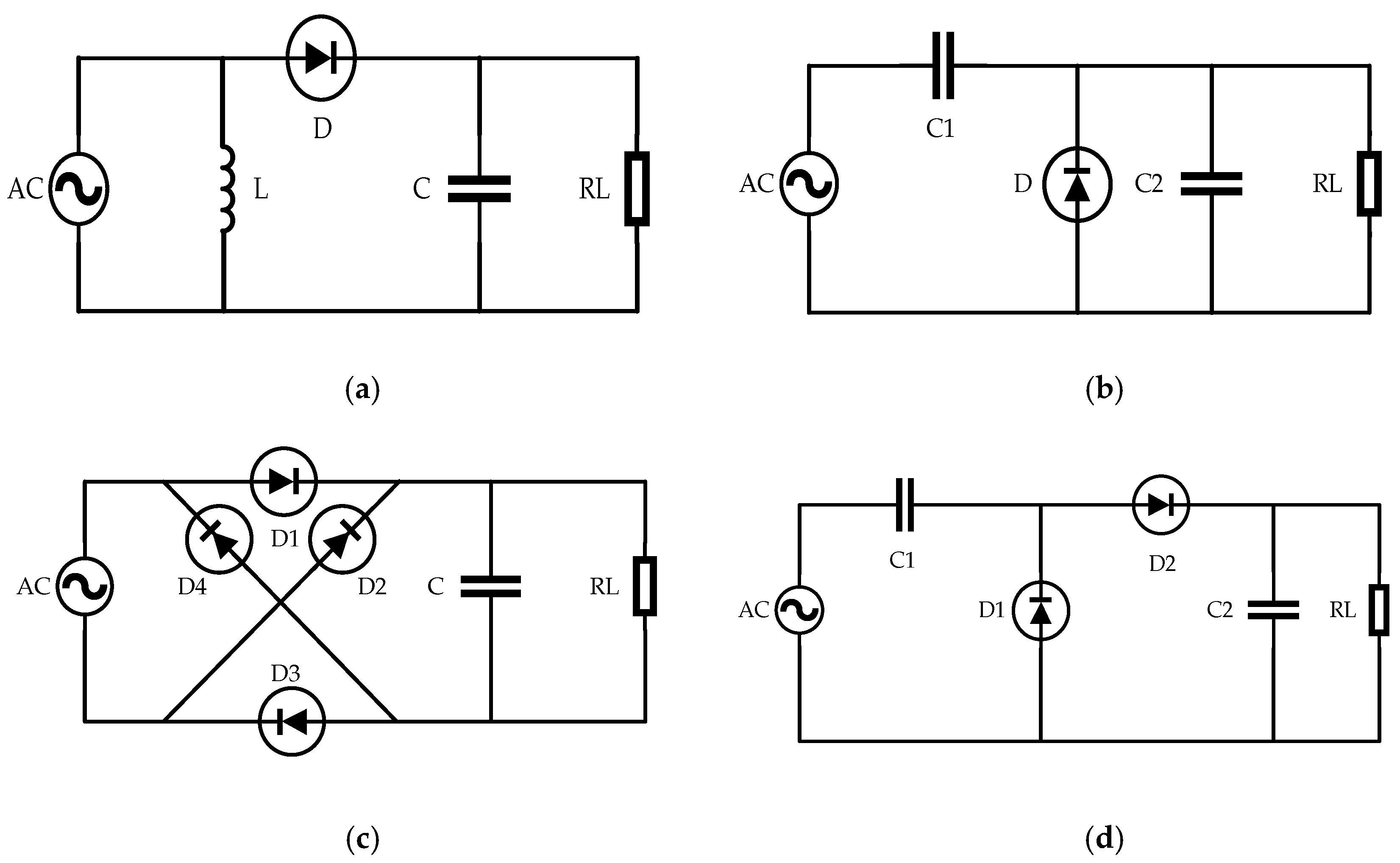
19], and its topological structure directly dictates the output voltage and power conversion efficiency. Common rectification topologies encompass single series and single shunt half-wave rectifiers, bridge rectifiers, and voltage multiplier rectifiers [
20], as schematically illustrated in
Figure 1.
Among these, although the single series diode rectifier shown in
Figure 1a and the single shunt diode rectifier in
Figure 1b feature simple configurations, they utilize only half a cycle of the input signal, resulting in a low output voltage and limited efficiency. The bridge rectifier in
Figure 1c, despite achieving full-wave rectification and enhanced output continuity, suffers from pronounced losses induced by the diode forward voltage drop under low-power RF input conditions, which restricts its practical application. In contrast, the voltage multiplier circuit achieves step-by-step voltage stacking through multi-stage capacitors and diodes, thereby delivering a higher DC output voltage than basic half-wave rectifier topologies [
21]. This feature makes voltage multiplier topologies suitable for compact RF rectifiers that require enhanced DC output while avoiding an additional active boost stage [
22].
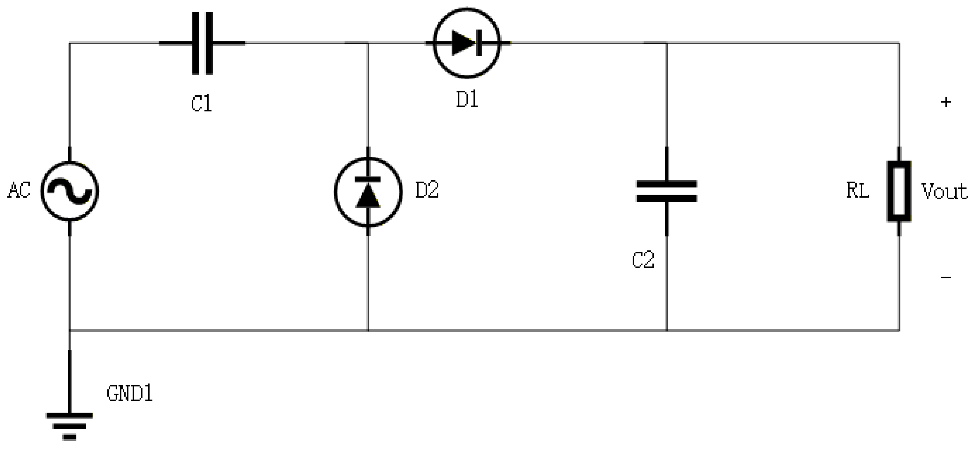
Consequently, considering the trade-off among output voltage, power conversion efficiency, component losses, and circuit complexity, a voltage-doubler topology is selected as the rectification circuit in this work, as shown in
Figure 2.
The circuit typically consists of two Schottky diodes, D1 and D2, and two energy-storage capacitors, C1 and C2. Its dynamic operation can be divided into two distinct phases. During the negative half-cycle of the input RF signal, diode D2 is forward-biased while D1 is reverse-biased; the current flows through D2 to charge capacitor C1, driving its voltage to gradually rise to the peak signal amplitude
. When the signal alternates to the positive half-cycle, D2 turns off due to the reverse voltage, and the input source voltage stacks in series with the stored voltage across C1. This combined voltage drives diode D1 to conduct, thereby supplying power to the load
and the filtering capacitor C2. The adopted voltage-doubler topology achieves voltage multiplication through the charging and discharging mechanisms of the capacitors, and its DC output voltage under ideal conditions,
, can be expressed as:
In the aforementioned formulation, represents the voltage amplitude of the input RF signal, while denotes the turn-on voltage of the diode. Equation (1) indicates that the voltage multiplier structure can effectively elevate the DC output level without introducing additional active boost components. However, under high-frequency operation at 2.45 GHz, the actual output voltage is inevitably deteriorated by the diode junction capacitance (), series resistance (), and the losses within the impedance matching network. To address this issue, an 11-segment microstrip distributed parameter network is introduced in this work. This network aims to compensate for these non-linear parasitic effects and precisely match the complex impedance of the diode, thereby maximizing the proximity to the theoretical gain value under heavy load conditions and providing a solid theoretical foundation for achieving a DC output exceeding 5 V.
2.2. Impedance Matching Network Design and Microstrip Line Optimization
In an RF rectification circuit, due to the non-linear characteristics of the Schottky diode and the coupling effects among multiple components within the voltage multiplier configuration, the input port exhibits a pronounced frequency-dependent complex impedance characteristic, which dynamically shifts with the varying input power levels. However, since RF systems typically employ a 50 Ω standard interface, the absence of an effective matching network will lead to severe reflection losses, thereby significantly degenerating the utilization efficiency of the RF energy. Therefore, an appropriate impedance matching network is required to reduce reflected power and improve RF power delivery to the rectifier. In this work, an analytical model of the voltage doubler rectifier circuit is first established at the schematic level. Through simulation, its input impedance near the target frequency of 2.45 GHz is extracted, and the impedance trajectory is subsequently analyzed using a Smith chart. On this basis, an L-type matching network featuring a simple topology and flexible adjustability is adopted to transform the input impedance. The network consists of a shunt inductor and a series capacitor, whose optimized parameters are approximately 3.9 nH and 2.6 pF, respectively. This configuration transforms the input impedance of the rectifier circuit toward the 50 Ω system impedance at the target frequency, thereby reducing input reflection and improving RF power delivery from the source to the rectification circuit.
However, in the GHz frequency band, traditional lumped-parameter matching methods can hardly reflect the distributed-parameter effects within the practical circuit accurately. Particularly in miniaturized designs, the impacts of trace lengths and layout configurations on circuit performance cannot be ignored. Continually utilizing ideal wires to connect components would introduce non-negligible discrepancies between the simulation results and the actual performance. To improve modeling accuracy, all ideal interconnects in the schematic are replaced with microstrip transmission line structures in this paper. The microstrip network was designed on a Rogers RO4350B substrate with a thickness of 0.51 mm, relative permittivity of 3.48, loss tangent of 0.0037, and copper thickness of 35 μm. Utilizing the LineCalc tool embedded in Advanced Design System (ADS, version 2024), the microstrip line width corresponding to the 50 Ω standard characteristic impedance is calculated to be 1.1 mm. Within the distributed-parameter model, the electrical performance of a microstrip line is primarily dictated by its electrical length
, and the analytical relationship between the electrical length
and its physical length
can be expressed as:
where
is the phase constant,
is the effective dielectric constant of the RO4350B substrate, and
is the free-space wavelength. Equation (2) indicates that fine compensation of both phase and impedance trajectories can be achieved by precisely adjusting the physical lengths of the microstrip lines.
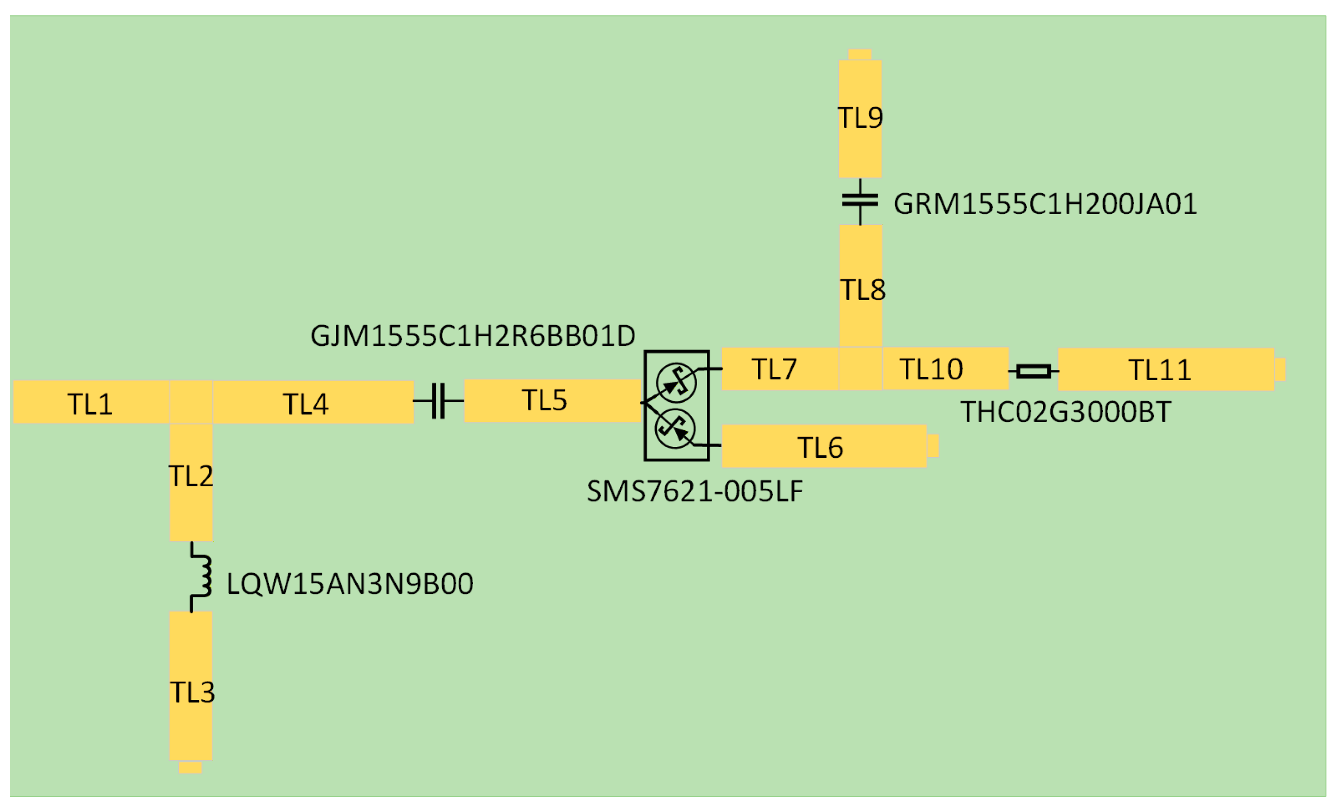
Based on this theory, eleven segments of microstrip lines are defined in this paper, with their lengths parameterized as variables through . By utilizing this multi-segment distributed parameter collaborative optimization method, the parasitic effects introduced by the diode packaging can be effectively counteracted. Furthermore, precise matching at the fundamental frequency is achieved within a compact area of only 3.48 cm × 1.98 cm, laying a solid foundation for obtaining a high output voltage of 5.42 V in practical measurements.
The eleven-segment division was not introduced simply to increase the number of adjustable transmission-line lengths. Instead, it was determined by the actual physical layout of the rectifier, including the RF input path, impedance-transition sections, diode-adjacent tuning sections, interconnection paths between the voltage-doubler components, and the DC filtering region as well as the load connection area. Therefore, the 11 segments represent physically distinguishable distributed microstrip sections rather than artificially inserted optimization variables. This segmentation allows the distributed transmission-line effects, local phase delay, impedance transformation, and diode parasitic compensation along the complete RF-to-DC path to be evaluated at the circuit-layout level.
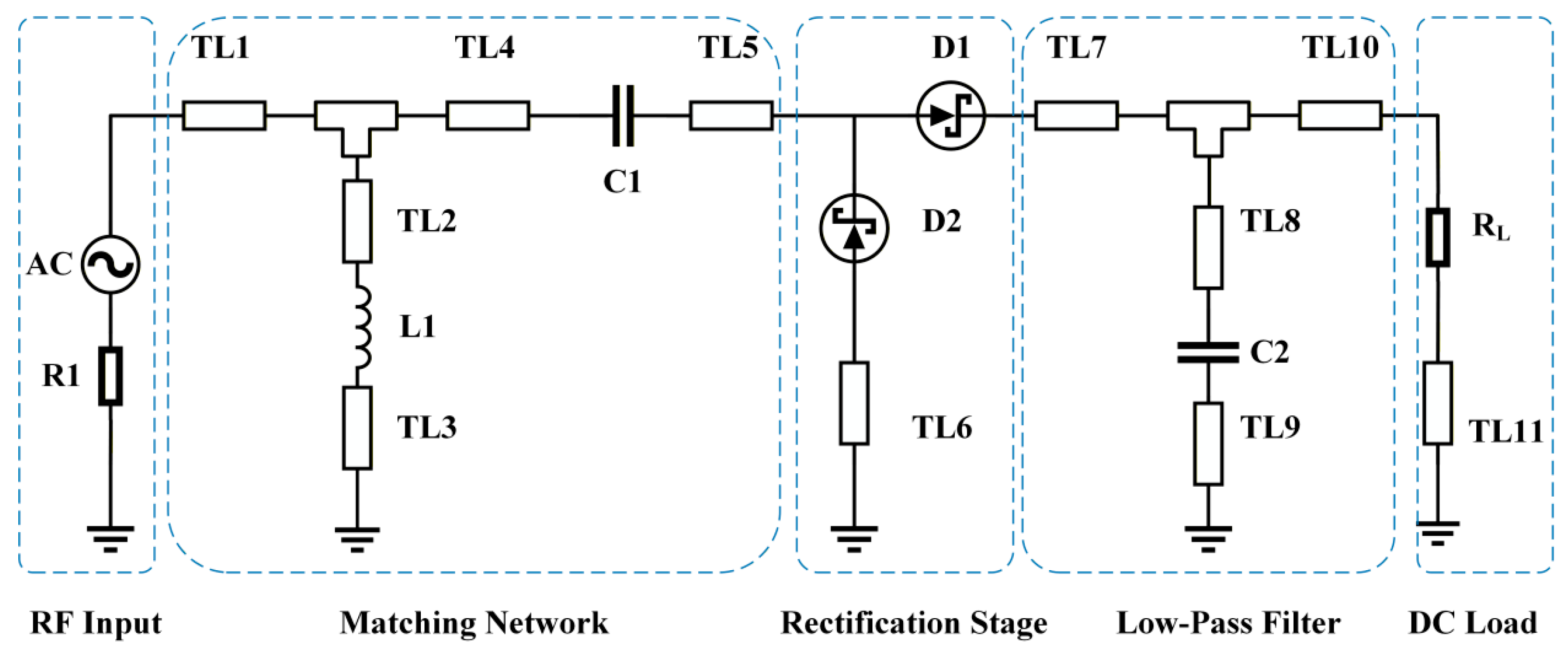
The topology of the matching network is illustrated in
Figure 3. Based on this configuration, a multi-variable collaborative optimization method is implemented to jointly adjust the lengths of each microstrip line segment, aiming to improve the impedance matching characteristics and overall rectifier performance. Through the co-optimization of the electrical lengths across multiple transmission lines, fine tuning of the input impedance is achieved, and the RF energy transmission path within the circuit is simultaneously optimized. The optimized dimensions for the 11 microstrip line segments are determined as follows: TL1 = 4.1 mm, TL2 = 3 mm, TL3 = 3.8 mm, TL4 = 5.1 mm, TL5 = 4.5 mm, TL6 = 5.2 mm, TL7 = 3 mm, TL8 = 3.1 mm, TL9 = 3 mm, TL10 = 3.2 mm, and TL11 = 5.5 mm.
Compared with conventional matching approaches that mainly rely on the adjustment of a limited number of matching elements or individual parameter tuning, the proposed method utilizes the distributed degrees of freedom provided by multiple microstrip-line sections and performs their collaborative optimization. This enables the circuit to achieve an improved matching state within the target frequency band while maintaining a compact physical size. Furthermore, the distributed-parameter-based matching optimization extends the frequency response range of the circuit to a certain extent, allowing it to maintain robust energy conversion capability over multiple operating frequencies.
To quantify the influence of the transmission-line parameters on circuit performance and further illustrate the differences between single-parameter tuning and the proposed collaborative optimization strategy,
Section 2.4 presents a microstrip-line sensitivity analysis and corresponding frequency-response comparisons. A detailed discussion of the parameter extraction process of the multi-segment microstrip matching network, the limitations of univariate optimization, and the implementation procedure of the multivariable collaborative optimization method is also provided in
Section 2.4.
2.3. Component Selection
In RF rectification circuits, since the operating frequency is in the GHz range, the parasitic parameters, quality factor, and high-frequency stability of components exert a critical influence on circuit performance. Consequently, during the component selection process, factors such as high-frequency performance, temperature stability, package size, and the availability of accurate simulation models must be comprehensively evaluated to minimize losses and maximize rectification efficiency. The detailed parameters of the selected key components are described below.
The SMS7621-005LF Schottky diode (Skyworks Solutions, Inc., Irvine, CA, USA) is selected as the core rectifying device. For compact RF rectifiers used in energy harvesting and dedicated RF-powered sensing applications, the high-frequency performance and switching loss of the rectifying device are strongly influenced by its cut-off frequency,
, which can be analytically expressed as:
where
represents the equivalent series resistance and
denotes the zero-bias junction capacitance of the diode. Compared to conventional silicon-based PN junction diodes or MOSFETs, the Schottky diode presents prominent circuit-level advantages. First, it features an ultra-low turn-on voltage of approximately 260–320 mV, which significantly lowers the conduction threshold under weak signals. Second, as a unipolar majority-carrier device, it exhibits negligible minority-carrier storage effects, resulting in a very short reverse recovery time and reduced reverse recovery-related losses during high-speed switching. Based on the equivalent-circuit approximation, the major high-frequency power losses of the diode,
, can be estimated as:
where
is the operational angular frequency;
represents the peak amplitude of the fundamental RF current flowing through the diode; and
denotes the peak amplitude of the fundamental RF voltage across the diode. Based on the aforementioned high-frequency loss mechanisms, the SMS7621 Schottky diode selected in this design features a maximum operating frequency of up to 24 GHz, a low barrier voltage, and a minimal junction capacitance (
= 0.10 pF). With an equivalent series resistance (
) of approximately 18
, this device supports effective rectification over the investigated input-power range and helps reduce the capacitive loss component triggered by the operational angular frequency
.
Nevertheless, inherent performance trade-offs exist for this device. Due to its relatively low reverse breakdown voltage and a temperature-dependent reverse saturation leakage current, the rectifier is susceptible to exacerbated reverse leakage at high input powers. This serves as the primary physical mechanism behind the degradation of rectification efficiency under large-signal or overdriven conditions. In comparison, while PIN diodes offer exceptionally high breakdown voltages, their larger threshold voltages make them less suitable for weak ambient RF energy harvesting. MOSFET-based rectifying structures can achieve reduced effective turn-on voltage through active biasing or advanced CMOS processes. However, they often require additional control circuitry and may introduce increased parasitic effects, thereby limiting their practicality in compact passive systems. Consequently, comprehensively balancing the high-frequency cut-off boundary, low-power conversion efficiency, and single-stage footprint compactness, the Schottky diode remains a suitable choice for this design.
Regarding capacitive components, the GJM1555C1H2R6BB01D high-frequency ceramic capacitor (Murata Manufacturing Co., Ltd., Nagaokakyo, Kyoto, Japan) is selected for the matching network. It features a capacitance of 2.6 pF in a 0402 package, utilizing C0G dielectric material. This class of capacitors offers extremely low dielectric loss and outstanding temperature stability, with a quality factor exceeding 452 and an ESR of approximately 300 mΩ, which helps mitigate energy loss during high-frequency signal transmission. For the filtering network, the Murata GRM1555C1H200JA01 capacitor (Murata Manufacturing Co., Ltd., Nagaokakyo, Kyoto, Japan) is employed, providing a capacitance of 20 pF and a temperature stability of 0 ± 30 ppm/°C, thereby effectively smoothing the rectified output voltage.
For inductive components, the LQW15AN3N9B00 high-frequency inductor (Murata Manufacturing Co., Ltd., Nagaokakyo, Kyoto, Japan) is adopted in the matching network. This inductor provides an inductance of 3.9 nH in a 0402 package, with a self-resonant frequency (SRF) greater than 10 GHz and a DC resistance (DCR) of approximately 0.07 Ω. Utilizing a high-frequency ceramic core structure, the device maintains stable inductive characteristics well into the GHz frequency band while exhibiting low loss, which is highly beneficial for enhancing the performance of the impedance matching network.
In terms of the load design, a THC02G3000BT thin-film resistor (Guangdong Fenghua Advanced Technology (Holding) Co., Ltd., Zhaoqing, China) is selected, featuring a resistance of 300 Ω in a 0402 package, with a tolerance of ±0.1% and a temperature coefficient of ±25 ppm/°C. Compared with thick-film resistors, thin-film resistors offer lower parasitic inductance and capacitance, maintaining a superior purely resistive characteristic under high-frequency conditions, thereby reducing signal loss and improving circuit stability.
2.4. Distributed Parameter Collaborative Optimization of Microstrip Lines and Methodology Analysis
Within the overall optimization framework, to fully exploit the energy harvesting potential of the rectifier across multiple frequency bands under a compact physical size, a multi-objective weighted composite efficiency evaluation function, F, is first constructed as the core metric for evaluating network performance:
where
= 2.4 GHz represents the primary operational frequency band, while
= 4.45 GHz and
= 7.15 GHz correspond to the higher-order resonant frequency bands excited by the matching network;
denotes the radio frequency-to-direct current (RF-to-DC) conversion efficiency of the rectifier circuit at frequency
; and
represents the weighting coefficient assigned to each respective frequency band. To ensure optimal power output of the rectifier within the core 2.45 GHz band while simultaneously accommodating the microwave energy harvesting potential in the higher frequency bands, the weighting coefficients are selectively configured as
= 0.6,
= 0.2, and
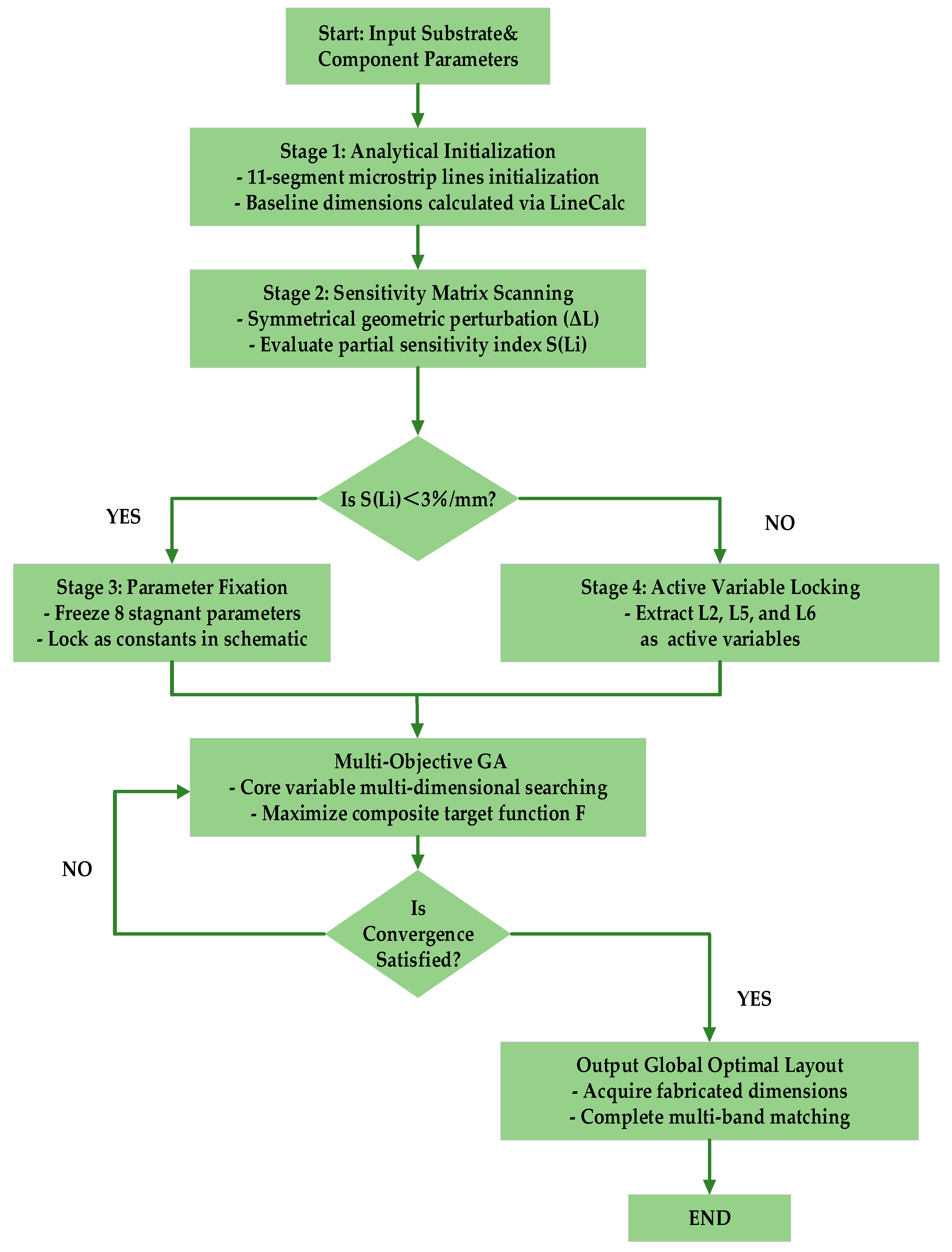
= 0.2. Driven by this evaluation metric, the specific collaborative optimization workflow progressively unfolds according to the timeline illustrated in
Figure 4.
Although eleven physical microstrip sections are included in the distributed model, the proposed method does not optimize all of them blindly. The purpose of the initial segmentation is to preserve the distributed electromagnetic behavior of the complete layout, whereas the subsequent sensitivity analysis identifies which sections actually dominate the rectifier response. First, prior to any sensitivity analysis or algorithmic exploration, the baseline physical dimensions for all 11 microstrip lines were simultaneously established using the LineCalc tool based on the commercial Rogers RO4350B substrate parameters (substrate thickness
= 0.51 mm, relative dielectric constant
= 3.48, loss tangent
= 0.0037, and copper foil thickness
= 35 um). To guarantee a standard 50 Ω characteristic impedance match, the physical width of the primary transmission traces was uniformized at 1.1 mm. The initial lengths of these 11 microstrip segments were analytically established as:
L1(0) = 4.1 mm,
L2(0) = 3.5 mm,
L3(0) = 3.8 mm,
L4(0) = 5.1 mm,
L5(0) = 4.0 mm,
L6(0) = 4.5 mm,
L7(0) = 3.0 mm,
L8(0) = 3.1 mm,
L9(0) = 3.0 mm,
L10(0) = 3.2 mm, and
L11(0) = 5.5 mm. Upon acquiring these initial boundaries, a control-variable, one-dimensional localized matrix scan was performed in the ADS environment. During each simulation run, only a single microstrip line length, Li, was varied by introducing a symmetrical geometric perturbation of
= ±0.5 mm relative to its LineCalc-derived analytical baseline
Li(0), while the physical dimensions of the remaining 10 microstrip lines were strictly clamped. To quantitatively evaluate the degree of disturbance exerted by the dimensional fluctuation of each segment on the multi-band composite rectification performance, a partial sensitivity index based on a bidirectional finite-difference scheme is introduced:
where the numerators respectively correspond to the absolute deviations of the composite target function, F, triggered by the forward and backward perturbations. The matrix scanning results reveal a distinctive two-tier bifurcation profile: the multi-band composite index F exhibits extreme stagnation toward dimensional variations in
L1,
L3,
L4, and
L7 to
L11, with all their partial sensitivity scores dropping safely below the specified threshold of 3%/mm. This behavior indicates that these eight microstrip segments primarily govern baseline impedance transitions and DC filtering, and their analytically derived placeholders are already sufficiently close to the optimum performance boundary. Driven by this quantitative filtering criterion, to eliminate computational redundancy, reduce the dimensionality of the optimization space, and accelerate algorithmic convergence, these eight insensitive geometric lengths are decisively excluded from the subsequent algorithmic synthesis. Instead, they are locked as layout constants within the schematic directly at their optimal LineCalc-derived analytical dimensions:
L1(0) = 4.1 mm,
L3(0) = 3.8 mm,
L4(0) = 5.1 mm,
L7(0) = 3.0 mm,
L8(0) = 3.1 mm,
L9(0) = 3.0 mm,
L10(0) = 3.2 mm, and
L11(0) = 5.5 mm. Conversely, owing to their critical locations at the key topological nodes for dynamic impedance tuning and non-linear compensation,
L2,
L5, and
L6 exhibit a dominant, high-sensitivity profile characterized by
S(Li) > 7%/mm. The sensitivity parameters for each microstrip line are presented in
Table 1.
To ensure the reproducibility of the parameter-selection process, the sensitivity classification threshold was explicitly defined based on the quantitative distribution of S(Li). Microstrip segments exhibiting S(Li) < 3%/mm were classified as low-sensitivity variables and invariant placeholders, which were frozen at their analytically derived baseline dimensions. Conversely, segments yielding S(Li) > 7%/mm were identified as the dominant tuning elements. Under this dual-threshold filtering criterion, L2, L5, and L6 were successfully extracted as the active three-dimensional variable vector for subsequent genetic-algorithm synthesis, while the remaining eight stagnant parameters were fixed to compress the dimensionality of the optimization space and accelerate algorithmic convergence.
Specifically, L2 adjacent to the RF signal input terminal is primarily responsible for the coarse adjustment of the impedance baseline and the initial matching of the reflection coefficient; L5 is situated in the middle section of the matching network, serving as a critical nexus to connect the preceding and succeeding stages while balancing the impedance distribution across both high- and low-frequency bands; meanwhile, L6 is positioned immediately adjacent to the anode input terminal of the SMS7621 Schottky diode, exerting the most direct tuning and compensation capabilities over the dynamic input capacitance and non-linear impedance of the diode. With the remaining eight redundant variables permanently frozen, L2, L5, and L6 are extracted as the active three-dimensional variable vector to directly invoke the built-in Genetic Algorithm optimization module within the Advanced Design System software (ADS, version 2024) for ultimate multi-variable refinement. Taking their theoretical LineCalc values (L2(0) = 3.5 mm, L5(0) = 4.0 mm, and L6(0) = 4.5 mm) as the analytical starting seeds, the GA engine is driven to maximize the composite evaluation function, max {F(L2, L5, L6)}, subject to strict physical boundaries of 3.0 mm ≤ Li ≤ 5.5 mm. To balance computational efficiency and convergence precision, the maximum number of iterations for the GA optimizer is uniformized at 100 with a desired error configured at 0.01. The optimization process terminates either when the global error between consecutive generations falls below the prescribed tolerance of 0.01 or when the iteration count reaches the maximum limit of 100 generations. Upon completing this heuristic, multi-variable self-adaptive evolution, the dimensions rapidly converge to the ultimate global layout solution: L2 = 3.0 mm, L5 = 4.5 mm, and L6 = 5.2 mm.
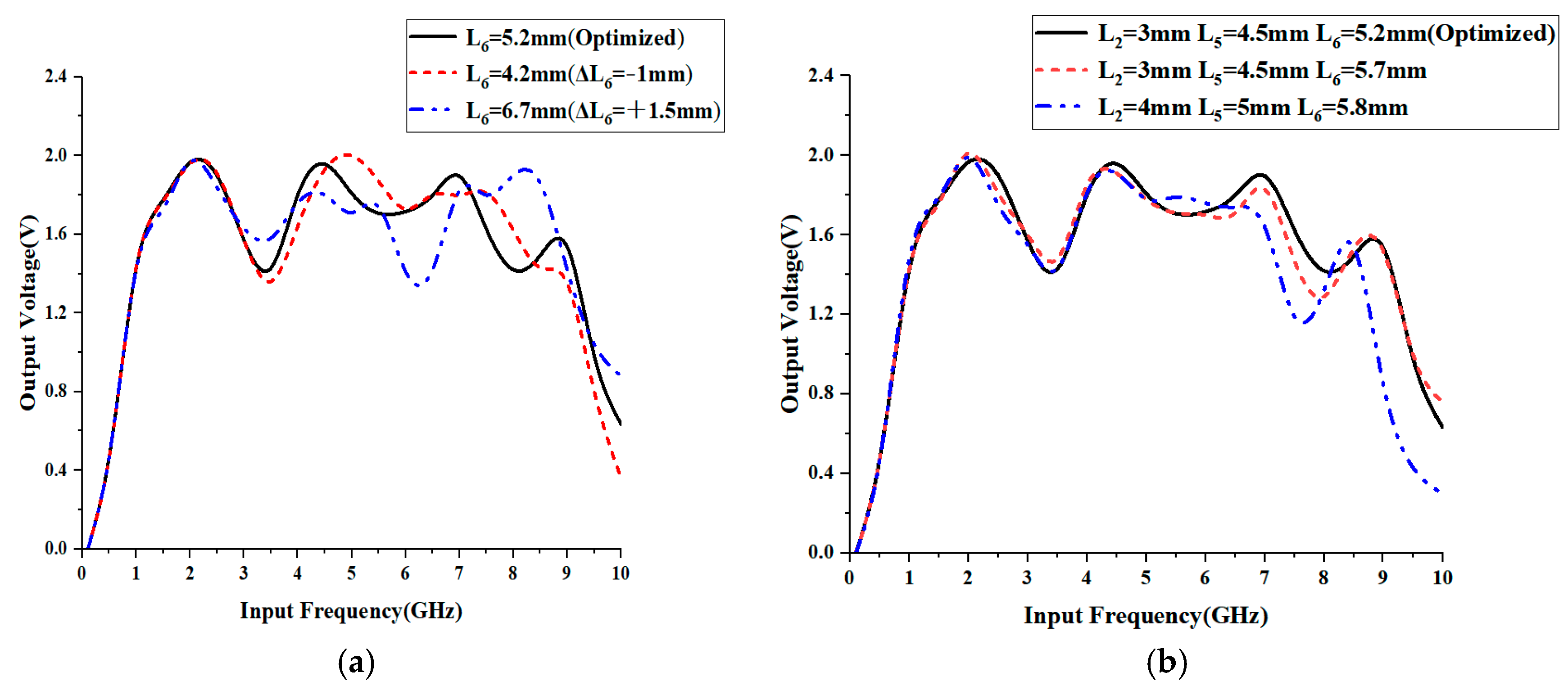
The frequency-response comparison in
Figure 5 illustrates the effect of the proposed collaborative optimization strategy compared with single-parameter tuning of an individual microstrip segment. As shown in
Figure 5a, varying only
L6 can shift the voltage peaks at different frequencies, but it cannot simultaneously maintain balanced responses over the multiple target bands. This indicates the limitation of univariate tuning, in which improving the response at one frequency may degrade the impedance condition at another frequency. In contrast, the joint adjustment of
L2,
L5, and
L6 in
Figure 5b provides a more balanced frequency response around the designed operating bands. To further evaluate the optimization behavior over a wider frequency range, the frequency response is analyzed from 0.1 GHz to 10 GHz. The collaboratively optimized multi-segment microstrip structure maintains higher output-voltage levels near the target bands, while the response decreases outside these bands due to deviation from the optimized impedance-matching condition. These results indicate that collaborative adjustment of multiple microstrip sections is more effective than single-parameter tuning for balancing distributed impedance transformation and multiband RF-to-DC response within the desired frequency range.
4. Experimental Results and Analysis
4.1. Measurement Environment
To verify the accuracy of the simulation results, the designed RF rectifier circuit was fabricated and measured. The circuit was implemented on a high-frequency PCB board and manufactured via a precision fabrication process using a standard commercial production line. The top layer of the substrate utilized Rogers RO4350B material (Rogers Corporation, Chandler, AZ, USA), on which fine metallic microstrip structures were etched. The bottom layer was covered with a large-area solid copper pour serving as a standard signal ground plane. The overall parameters of the substrate were as follows: a thickness of 0.51 mm, a relative permittivity of 3.48, a loss tangent of 0.0037, and a copper foil thickness of 35 . These parameters ensured high-frequency processing accuracy and minimized dielectric losses during energy transmission within the GHz frequency band. Concurrently, all critical lumped components were selected in 0402 surface-mount packages to significantly mitigate high-frequency parasitic effects. To achieve excellent RF shielding and low-loss signal return, grounded metallic vias were appropriately disposed between the top and bottom copper layers of the circuit, featuring an outer diameter of 24 mil (approximately 0.61 mm) and an inner diameter of 12 mil (approximately 0.30 mm). Additionally, a 50 edge-launch SMA RF connector was precisely soldered to the RF input port of the circuit to achieve a low-reflection, standard impedance-matched connection with the coaxial cable.
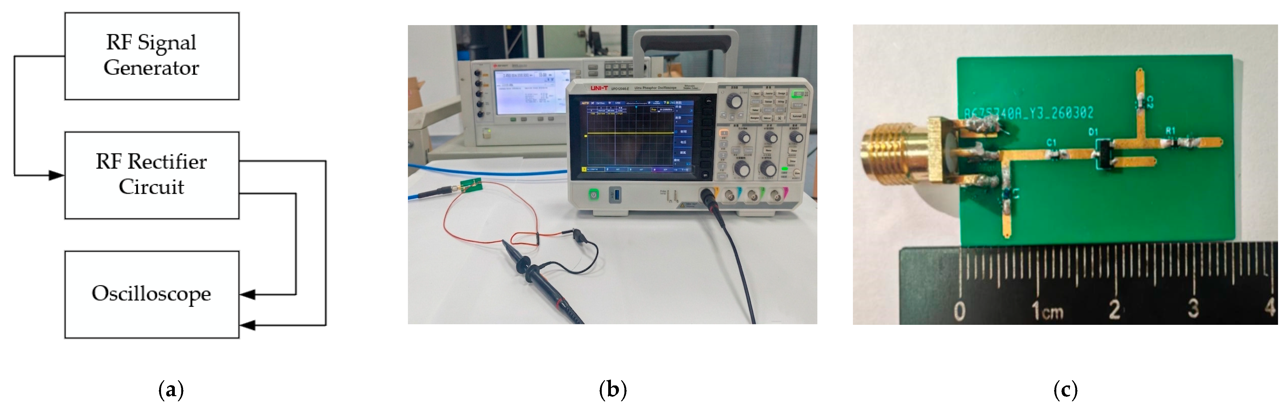
The complete experimental measurement system consisted of an RF signal generator, a coaxial cable, the fabricated RF rectifier circuit board, and an oscilloscope. In the specific experimental validation, a KEYSIGHT E8267D microwave vector signal generator (Keysight Technologies, Santa Rosa, CA, USA) was employed as the core excitation source to provide high-precision microwave signals. After the signals were fed into the rectifier board through a low-loss coaxial cable, a UPO1204X-E digital oscilloscope (UNI-TREND TECHNOLOGY (CHINA) CO., LTD., Dongguan, China) was utilized to capture the steady-state DC voltage across the load resistor in a real-time and accurate manner. Prior to the actual measurement, the parasitic insertion loss introduced by the coaxial cable and the SMA connector was precisely calibrated and compensated for at the signal generator side, thereby ensuring that the input RF power could be accurately delivered to the input reference plane of the rectifier circuit. The block diagram of the measurement system, the overall experimental setup, and the photograph of the fabricated RF rectifier circuit are illustrated in
Figure 10a–c, respectively.
During the testing process, the RF signal generator first delivers a 2.45 GHz RF signal, and the input power is adjusted to gradually increase from −20 dBm to 25 dBm. The DC voltage at the output terminal of the rectifier circuit is measured, and the rectification efficiency is calculated according to (7) to obtain the power characteristics of the circuit. Subsequently, the input power is fixed at 15 dBm, and the frequency of the input signal is swept from 0.1 GHz to 10 GHz to analyze the frequency response characteristics of the circuit. Through the aforementioned testing methodology, a comprehensive evaluation of the overall performance of the rectifier circuit is achieved.
4.2. Measured Data
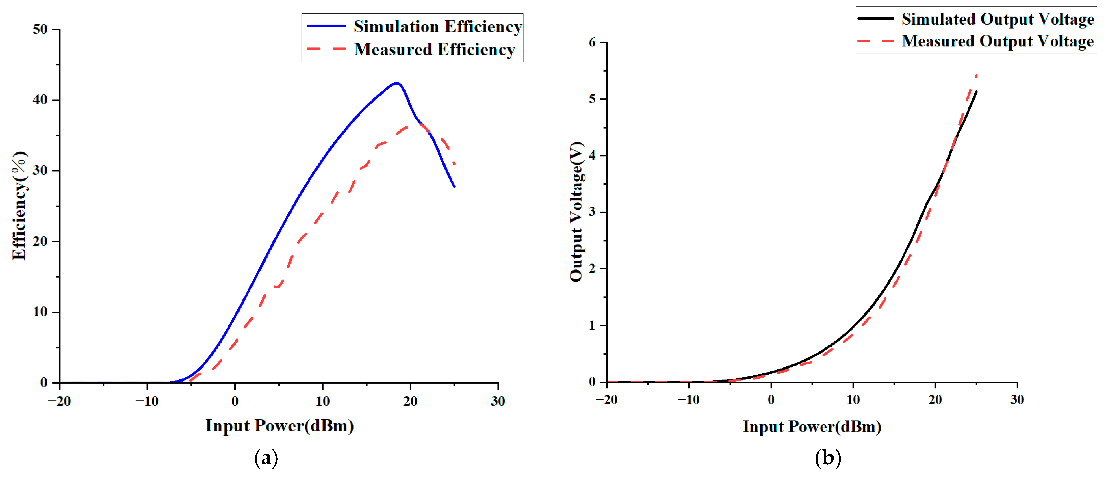
The comparison curves between the simulated and measured results are presented in
Figure 8. As can be observed from the efficiency comparison in
Figure 8a, the measured rectification efficiency is generally lower than the simulated results, though the overall trends remain highly consistent. At an input power of approximately 20 dBm, the measured efficiency reaches 36.3%, which is close to the simulated prediction.
The voltage response illustrated in
Figure 8b clearly indicates that the output voltage exhibits a favorable monotonically increasing relationship with the input power. Within the input power range of 24 to 25 dBm, the measured output voltage ranges from 5.05 to 5.42 V, which is in good agreement with the simulation results, thereby validating the effectiveness of the voltage-doubler rectifier configuration in achieving high output voltages. Notably, under a 25 dBm input at 2.45 GHz, the maximum measured DC output voltage reaches 5.42 V across the 300 Ω load. This load resistance simulates the equivalent input impedance of typical low-power wireless sensor nodes operating in active or data-transmission modes. The resulting output current of 18.07 mA and delivered power of 97.92 mW demonstrate strong load-driving capability under the tested high-input-power condition, indicating that the rectifier can support low-power Microcontroller Unit (MCU) or sensor-node loads in controlled RF powering scenarios without a subsequent DC-DC boost stage.
It should be noted that the 25 dBm input power used to demonstrate the 5 V direct load-driving capability is higher than the RF power level typically available in most ambient RF energy harvesting environments. In practical ambient harvesting scenarios, the received RF power strongly depends on the distance from the transmitter, antenna gain, propagation loss, polarization mismatch, and surrounding electromagnetic conditions. Therefore, the 5 V direct-driving result should be interpreted as a demonstration of the power-handling and load-driving capability of the proposed rectifier under controlled or dedicated RF excitation, rather than as a guaranteed output level under arbitrary ambient RF conditions. Under lower input power levels, the proposed rectifier still exhibits useful RF-to-DC conversion behavior, as indicated by the simulated efficiency above 40% in the 15–20 dBm range and the measured multiband response at 15 dBm. However, for weak ambient RF environments, practical operation would more likely require energy accumulation through a storage element, duty-cycled sensor operation, or integration with a power management unit.
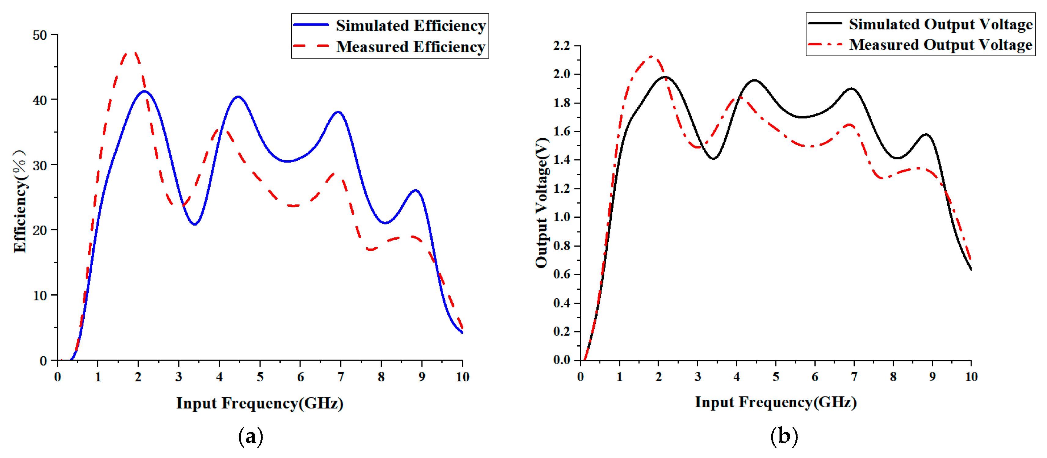
Furthermore, the comparison results illustrated in
Figure 9 indicate that the overall trend of the measured frequency response curve aligns well with the simulated curve, despite certain offsets in both peak positions and amplitudes. The peak output voltage shifted from the simulated 2.1 GHz to the measured 2 GHz where the optimal performance was achieved. This demonstrates that the multi-frequency response characteristics of the fabricated circuit are fundamentally consistent with the simulation predictions, with minor discrepancies attributed to practical environmental factors.
4.3. Load-Dependent Performance Analysis
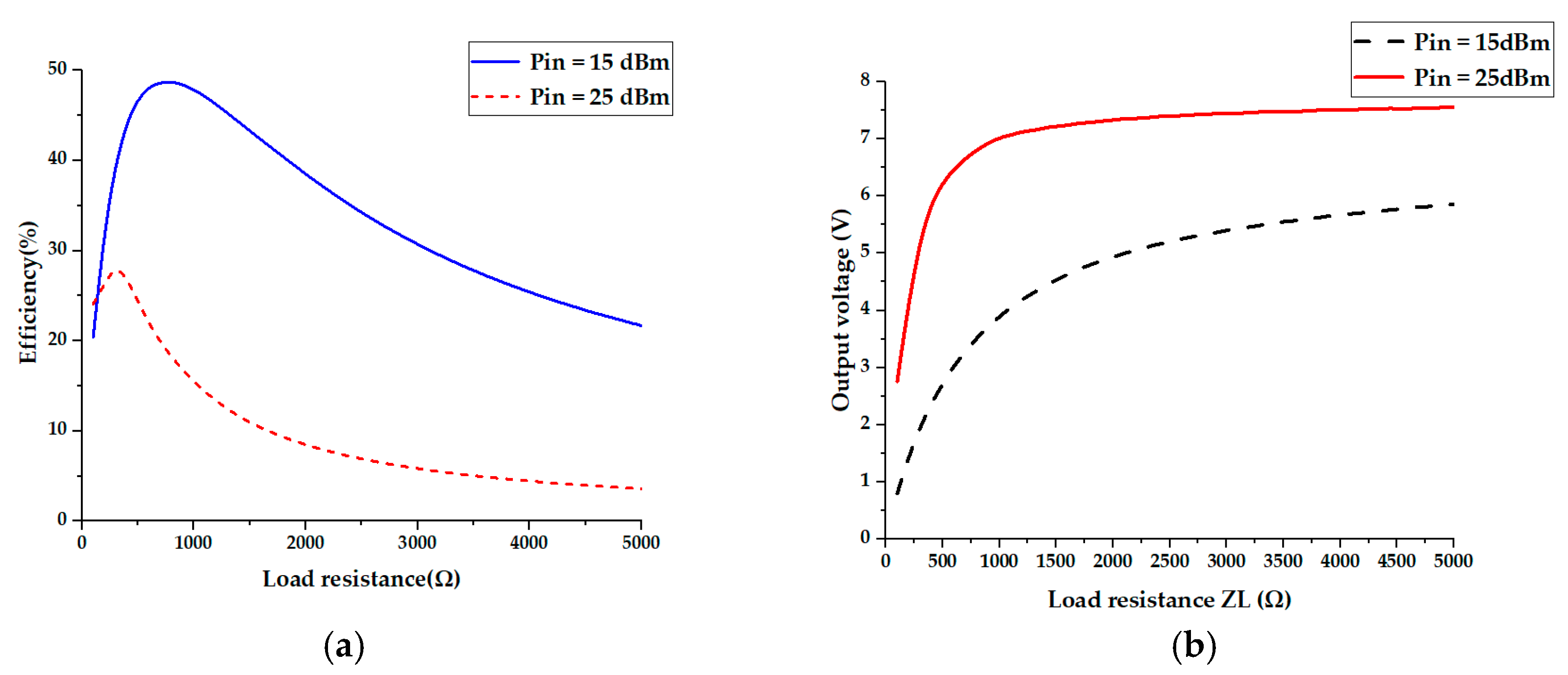
In addition to input power and frequency response characteristics, load impedance is another crucial factor affecting the RF-to-DC rectification performance. Therefore, the output characteristics of the proposed rectifier under varying load conditions are further investigated. At the operating frequency of 2.45 GHz, a load sweep analysis was conducted under two representative input power levels of 15 dBm and 25 dBm, with the resulting profiles illustrated in
Figure 11. Specifically,
Figure 11a and
Figure 11b plot the variations in rectification efficiency and DC output voltage across a range of load resistances, respectively.
As observed from the efficiency curves in
Figure 11a, the rectification efficiency exhibits a distinct non-linear characteristic with respect to the load resistance. Under 15 dBm input power, the rectification efficiency initially increases with the load resistance, reaching its maximum value within the range of approximately 700–900 Ω; as the load continues to increase, the efficiency gradually declines. This behavior occurs because the load impedance governs the voltage and current distribution at the rectifier’s output port, where either an excessively low or high load leads to a degradation in the RF-to-DC energy conversion efficiency. Meanwhile, the voltage response illustrated in
Figure 11b shows that the output voltage increases monotonically with the load resistance. This trend is attributed to the fact that a larger load impedance relaxes the output current requirement, allowing more charge to accumulate on the output filtering capacitor.
Under 25 dBm input power, the rectifier exhibits a significantly higher output voltage level across the entire load range. At a load resistance of 300 Ω, the output voltage reaches 5.134 V, corresponding to an output current of 17.1 mA and a delivered DC output power of 87.9 mW. This low-resistance load condition imposes a more stringent demand on the current delivery capability of the rectifier, supporting its heavy-load driving performance under the specified high-input-power condition.
4.4. Discrepancy Analysis
The deviations observed between the simulated and measured results can be primarily attributed to the combined effects of several factors. First, the diode and passive component models utilized during the simulation process are mostly idealized or semi-empirical. In particular, conventional SPICE models typically describe only the electrical characteristics of a single diode junction without fully accounting for the package-induced parasitic inductances and capacitances. Consequently, it is challenging to accurately reflect the true behavior of the devices in the GHz frequency range. Although some parasitic parameters were introduced in subsequent simulations for correction, completely equivalent modeling of the complex high-frequency characteristics of the actual devices remains difficult to achieve.
Second, the SPICE models provided by manufacturers are generally intended for low-power, small-signal conditions. The typical characteristics in their datasheets are mostly based on testing conditions around 1.8 GHz and an input power not exceeding 10 dBm. In contrast, the circuit presented in this work operates at a higher frequency and across a wider input power range, exceeding the strict boundaries of the model’s applicability, which constitutes another significant reason for the simulation-to-measurement discrepancies.
Third, during the practical circuit implementation, PCB fabrication tolerances and microstrip line dimensional variations directly affect the impedance matching. Concurrently, the soldering process and connection methods introduce additional parasitic inductances and resistances, while the transmission losses along the cables and connectors are also non-negligible, thereby reducing the actual energy transmission efficiency. In addition, thermal factors also impact the circuit performance. Simulations are typically conducted based on a standard ambient temperature (approximately 25 °C); however, during actual operation, conduction losses in the diode lead to an increase in device temperature. This alters critical parameters such as the reverse saturation current and junction capacitance, further affecting the rectification performance.
Finally, factors such as the measurement accuracy of the testing system itself, cable losses, and external environmental interference also exert a certain influence on the experimental results. Despite these aforementioned sources of error, the overall trends of the simulated and measured results remain consistent, demonstrating that the proposed circuit design methodology and optimization strategies possess robust validity and engineering feasibility.
4.5. Performance Comparison and Analysis
Because RF rectifier performance is strongly dependent on operating frequency, input power, load resistance, rectifier topology, impedance matching condition, substrate, diode type, and measurement setup, a direct one-to-one comparison of peak efficiency or output voltage across different studies may be misleading. Therefore,
Table 2 is used as a structured benchmarking summary rather than an absolute performance ranking. The comparison focuses on operating frequency, diode selection, topology and impedance matching configuration, input power level, load resistance, peak power conversion efficiency, direct 5 V-class driving capability, and physical dimensions, allowing the proposed design to be evaluated in terms of its overall trade-offs under the specified test conditions.
Table 2 compares the proposed rectifier with previously reported designs. It should be noted that the peak RF-to-DC conversion efficiency of the proposed rectifier is not the highest among the compared works; several reported rectifiers achieve higher efficiencies under their respective optimized frequency, input-power, and load conditions. However, the proposed design exhibits a balanced performance profile by combining multiband rectification behavior, compact physical dimensions, and heavy-load driving capability. Specifically, the rectifier maintains conversion efficiencies of 39.11%, 40.55%, and 38.45% at 2.45 GHz, 4.45 GHz, and 7.15 GHz, respectively, whereas many referenced designs mainly focus on single-band or dual-band operation. Within the benchmarking scope of
Table 2, the proposed circuit also shows favorable structural compactness, particularly when compared with the multi-frequency designs reported in [
5,
8].
The proposed rectifier further delivers a 5 V-class output under the tested 25 dBm input and 300 Ω load condition, indicating its heavy-load driving capability under controlled RF excitation. A similar logic-driving capability is reported in [
20], but that design uses a more complex 2-stage series-parallel hybrid voltage doubler configuration and does not disclose its physical dimensions. In contrast, the proposed structure achieves 5 V-class load-driving performance using a single-stage voltage-doubler configuration combined with the 11-segment microstrip optimization network, without requiring a subsequent DC-DC boost stage. Overall,
Table 2 should be interpreted as a comparison of design trade-offs rather than a strict quantitative superiority comparison. Under this benchmarking framework, the proposed rectifier provides a compact multiband rectification front end with 5 V-class load-driving capability under the specified high-input-power condition.