Article

Simulated On-Board AI-Based Classification of Radiation-Induced SRAM Event Upsets

1
Department of Electronics and Computers, Faculty of Electrical Engineering and Computer Science, Transilvania University of Brasov, 500036 Brasov, Romania
2
Department of Telecommunications and Electronic Systems, Faculty of Electronics and Telecommunications, Technical University of Moldova, MD-2004 Chisinau, Moldova
*
Author to whom correspondence should be addressed.
Electronics 2026, 15(13), 2814; https://doi.org/10.3390/electronics15132814
Submission received: 21 May 2026 / Revised: 18 June 2026 / Accepted: 23 June 2026 / Published: 26 June 2026

Abstract

Radiation monitoring with SRAM-based FPGAs traditionally relies on offset-histogram analysis, which requires a chip-specific calibration campaign at an accelerator before multiple-cell upsets (MCUs) can be discriminated from coincident single-cell upsets (SCUs). The cost and complexity of such calibration restrict the approach to dedicated, beam-test-funded programs. We propose an AI-based on-board classifier that achieves MCU/SCU discrimination directly, without any chip-specific calibration. A lightweight Multi-Layer Perceptron (MLP), trained entirely on synthetic data covering five representative bit-interleaving layouts, is integrated on an AMD Artix-7 XC7A200T FPGA together with per-detection-element telemetry aggregation. The classifier achieves F1 = 0.92–0.97 on structured BRAM layouts when per-chip calibration data are available (calibrated ceiling) and, without any chip-specific calibration, retains F1 up to 0.81 ± 0.02 (held-out, mean over five seeds) on previously unseen layouts with near-perfect recall. A sensitivity analysis across a 20 × range of SEU rates and a 4 × range of MCU fractions confirms the robustness of the proposed approach. A feature-ablation study identifies an indispensable feature subset, while a comparative evaluation of four alternative classifier architectures (decision tree, support vector machine (SVM), two MLP variants) establishes the reference MLP as the optimal choice. Post-implementation results on the Artix-7 200T show that the MLP-enhanced and calibrated-histogram designs occupy nearly identical FPGA footprints, reframing the choice between them as an operational decision driven by calibration availability rather than by hardware cost.

1. Introduction

Semiconductor devices operating in space are continuously exposed to ionizing radiation from three principal sources: galactic cosmic rays (GCRs), solar energetic particles (SEPs), and charged particles trapped in the Van Allen radiation belts [1]. Galactic cosmic rays consist predominantly of protons (up to 90%), helium nuclei (up to 13%), and high-energy heavy ions (less than 1%). In low-Earth orbit (LEO), the dominant component of the background radiation is protons with energies from 10 MeV to 1 GeV, whereas in geostationary orbits (GEO) a significant contribution is made by electrons with energies up to several MeV. The flux of cosmic rays is modulated by the Earth’s magnetic field and solar activity, reaching a maximum in the polar regions during periods of quiet Sun.
The interaction of ionizing radiation with semiconductor circuits results in two categories of effects: cumulative and single-event. The cumulative effects, characterized by the total ionizing dose (TID), manifest as irreversible degradation of the electrical parameters of the device [2,3]. Single-event effects (SEEs) arise when a single charged particle traverses a sensitive region of the silicon substrate: the ionization trace generates a charge that, when exceeding a critical threshold ( Q CRIT ), can change the state of a memory element. The most significant types of SEE include single-event upset (SEU), single-event functional interrupt (SEFI), single-event transient (SET), and single-event latchup (SEL) [1,4].
Of particular interest in radiation monitoring are multiple-bit upsets (MBUs), in which several bits invert. These inversions may be caused by multiple particle strikes, each affecting a single physical memory cell, termed a single-cell upset (SCU), or a single particle strike affecting multiple adjacent cells, termed a multiple-cell upset (MCU) [5], or a combination of the two. MCUs have a higher occurrence rate in newer, denser, and under-20 nm technologies [6,7]. Classifying MBUs into SCUs and MCUs is operationally important because MCUs pose a direct threat to error-correction codes (ECCs), which are typically designed to correct only single-bit errors within a single memory word [8].
Field-programmable gate arrays (FPGAs) based on SRAM technology represent an attractive platform for ionizing radiation detection owing to their unique combination of properties: reconfigurability, hardware parallelism, direct access to internal memory resources, and the ability to implement low-latency AI inference with limited power consumption. Unlike application-specific integrated circuits (ASICs), FPGA development is characterized by shorter timescales and lower non-recurring engineering costs, and its granular architecture enables parallel data processing at throughput levels that exceed those of software implementations on general-purpose microprocessors. These qualities underpin the widespread adoption of FPGAs in both the space industry and high-energy physics experiments, for example, at CERN particle accelerators [1].
The fundamental feature of SRAM-based FPGAs is that all principal on-chip resources (i.e. block RAM-BRAM, look-up tables-LUTs, flip-flops-FFs, and configuration memory-CRAM) are implemented using static memory cells that are inherently sensitive to SEU [8]. This property gives rise to the concept of dual use: the FPGA simultaneously serves as the array of detection elements and as the processing platform that classifies the detected upsets. By writing a known data pattern into BRAMs and periodically scanning their contents, it is possible to detect, localize, and quantify SEUs using the BRAM primitives themselves as detection elements (DEs) [9]. Modern AMD FPGA families such as UltraScale+ devices, also provide other memory types suitable for detection, including distributed look-up table RAM (LUTRAM) and UltraRAM (URAM) [10].
The SEU sensitivity of an FPGA to radiation is quantitatively described by the effective cross-section σ SEU , which determines the probability of an SEU occurring when a particle traverses the volume of a memory cell. For the BRAM of AMD Artix-7 devices (28 nm), the neutron cross-section is 6.32 × 10 15  cm2/bit according to irradiation data at the LANSCE facility [11]. For heavy ions, the BRAM saturation cross-section in a 28 nm Xilinx Kintex-7 reaches 7.94 × 10 9  cm2/bit [12]. Testing of Artix-7 devices (i.e., XC7A100T) with 20 MeV electrons revealed a SEU cross-section of 10 17 10 18  cm2/bit, which is about five orders of magnitude lower than that for equivalent-energy 20 MeV protons [13].
In addition, experiments with 1–5 MeV electrons on the 28 nm Virtex-7 (XC7VX690T, also 28 nm) revealed a resonant nature of sensitivity: irradiation with 3 MeV electrons caused over 28.6 million SEUs in CLBs and 1.76 million SEUs in BRAMs, while at other energies (1, 2, 4, 5 MeV) no effects were registered [14]. A substantial proportion of these events produce MBUs, as detailed in Section 2.1.
To ensure stable operation of the FPGA device under radiation, mitigation mechanisms are employed: triple modular redundancy (TMR) [15,16] with physical separation [17], ECCs for memories [18], temporal redundancy [19], continuous scrubbing of the configuration memory [20,21], and radiation hardening by design [22].
In our prior work [9,23], we presented the AICoRS (AI-enabled Cosmic Radiation Sensor) system, implemented on the Artix-7 200T FPGA and intended for installation on a nanosatellite. The system performs parallel scanning of 256 detection elements at a frequency of 1 kHz, detects and corrects SEUs, and transmits the registered events via the SPI interface to the on-board computer (OBC). However, a detailed analysis of the implementation revealed several significant limitations. First, the 256-word deep first-in first-out (FIFO) buffer creates conditions for data loss whenever the number of detected SEUs in a single scan cycle exceeds the buffer capacity. Second, the priority encoder processes only one detection element per clock cycle, leading to collisions when multiple DEs simultaneously detect errors at the same addresses; in such cases, only one event is registered, and the others are lost. Third, the buffer overflow event is not reported to the OBC due to throughput limitations, leaving it unaware of lost events. Finally, the system operates in a single mode without any adaptation to the particle-flux intensity and performs no on-chip data analysis: all events are transmitted in raw form, without aggregation, clustering, or classification.
These limitations become especially significant under conditions of elevated background radiation intensity—during passage through the South Atlantic Anomaly (SAA), during solar flares, or during ground-based accelerator testing—when the SEU rate can increase by several orders of magnitude. In such scenarios, the current architecture inevitably loses a significant portion of the scientifically most valuable data, making it impossible to accurately estimate the particle flux and classify radiation events. Furthermore, the absence of on-chip MCU/SCU classification means that the existing system cannot distinguish between single-particle multi-cell events and coincident single-cell upsets. Statistical methods based on offset-histogram analysis [24] achieve excellent accuracy (F1 > 0.99) on structured BRAM layouts by automatically discovering repeatable offset patterns—the method is topology-invariant and does not require prior knowledge of the physical interleaving scheme. However, it requires a chip-specific calibration campaign to build the statistical model: until this process is complete, classification output is unavailable (the cold-start problem), and a different device necessitates repeating the procedure at an accelerator facility.
A preliminary account of this work, focused on system architecture and FPGA feasibility, has been accepted for presentation at the European Space Agency (ESA) SPAICE 2026 Conference [25]. The present paper substantially extends that contribution by providing a complete, detailed experimental setup (Section 4), sensitivity and feature-ablation analyses (Section 6.2 and Section 6.3), a comparative evaluation of four alternative classifier architectures (Section 6.6), and a detailed three-way post-implementation FPGA study (Section 5).
The synthetic data-generation methodology used in this work is listed as one of the contributions of another manuscript [26] submitted to a different journal at the same time as this one. For completeness, this manuscript also contains a description of this method.
In this paper, we propose an improved AICoRS architecture that addresses the identified limitations through the integration of on-chip AI inference and per-detection-element telemetry aggregation. The main contributions are as follows:
1.
System-level improvement: On-chip classification combined with per-DE aggregation replaces the raw per-upset streaming of the baseline architecture. Each detection element transmits a single classified summary packet per scan cycle, eliminating FIFO overflow and providing the OBC with real-time SCU/MCU event counts that previously required ground-based post-processing.
2.
Calibration-free on-chip MLP classifier: A lightweight MLP (8 → 32 → 16 → 1, 833 INT16 parameters, Q8.8 fixed-point) provides non-zero classification capability from first power-on without chip-specific calibration, achieving a mean F1 score of 0.807 (95% CI: 0.786–0.828; five random seeds) with near-perfect mean recall on an unseen structured layout under the held-out protocol (Section 4) in synthetic experiments—a scenario where the offset-histogram method, without prior calibration, yields no usable output.
3.
Complete FPGA implementation and three-way resource characterization: The baseline, offset-histogram, and MLP-enhanced designs are all implemented and compared post-implementation on the Artix-7 200T (Section 5), showing that the two classifiers occupy virtually the same silicon footprint and thermal envelope, making the selection an operational rather than a hardware-constrained decision. To support reproducibility, the complete hardware description language (HDL) implementation, trained classifier weights, and synthetic-data generation scripts are openly available on Zenodo (see the Data Availability Statement).

2. Background

This section provides the technical context required for the rest of the paper. Section 2.1 introduces the radiation-physics distinction between single- and multiple-cell upsets and explains why the proprietary BRAM bit-interleaving scheme prevents direct geometric inference of physical adjacency from the logical coordinates seen by the scan logic. Section 2.2 summarizes the AICoRS hardware platform on which the present work builds, and Section 2.3 reviews the offset-histogram method that serves as the calibrated baseline against which the proposed MLP classifier is evaluated.

2.1. SCU vs. MCU and Bit Interleaving

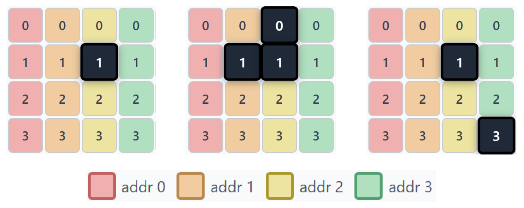
When a charged particle traverses the sensitive volume of an SRAM cell, the deposited charge may exceed the critical threshold Q CRIT and flip the stored bit value [4]. In modern deep-submicron processes, the charge cloud generated along the ionization track can extend laterally to adjacent cells. If the deposited charge is collected by a single cell, the event is an SCU; if multiple physically neighboring cells are upset by the same particle strike, the event is an MCU. Both SCU and MCU produce observable Bit Upsets (BU) in the memory content. The physical distinction between these cases, together with the operationally relevant case of coincident, independent SCU events that produce an MBU observation indistinguishable from an MCU on the basis of logical coordinates alone, is illustrated in Figure 1.
When a scan cycle detects more than one BU, the observation is classified as an MBU. An MBU may result from a single MCU or from the temporal coincidence of two or more independent SCU events within the same scan window. Following JEDEC JESD89A terminology [24], the classification task addressed in this paper is to determine whether a given pair of BUs within one scan originate from a common particle strike MCU or from independent impacts (coincident SCU).
The distinction is practically significant because MCU events can corrupt multiple bits within the same ECC word, defeating single-error-correcting codes that protect BRAM content [8]. In 28 nm Xilinx FPGAs of the Artix/Kintex family, irradiation studies have shown that up to ∼38% of ion, proton, and neutron events cause multiple configuration cells to be upset at high LET (60 MeV·cm2/mg), with a small fraction (a few percent) affecting four or more cells [24,27]. Accurately identifying MCU events is therefore essential both for radiation-environment characterization and for assessing the adequacy of on-board error-correction strategies.
A fundamental obstacle to on-chip MCU identification is the bit-interleaving scheme applied within FPGA block RAM primitives. BRAM manufacturers deliberately scatter logically consecutive bits across physically non-adjacent locations so that a single-particle MCU affecting a cluster of neighboring physical cells produces errors in different ECC words rather than in the same word. While this interleaving strategy strengthens ECC protection, it creates a non-trivial mapping between the logical address space (addr, bit) visible to the scan logic and the physical position of each cell on the silicon die. The exact mapping function is proprietary and is not disclosed in public documentation [28]. Consequently, two BU that appear at distant logical addresses may in fact originate from adjacent physical cells (and vice versa), making it impossible to infer physical proximity—and hence MCU membership—directly from the logical coordinates without prior knowledge of the chip-specific interleaving pattern.

2.2. The AICoRS System Architecture

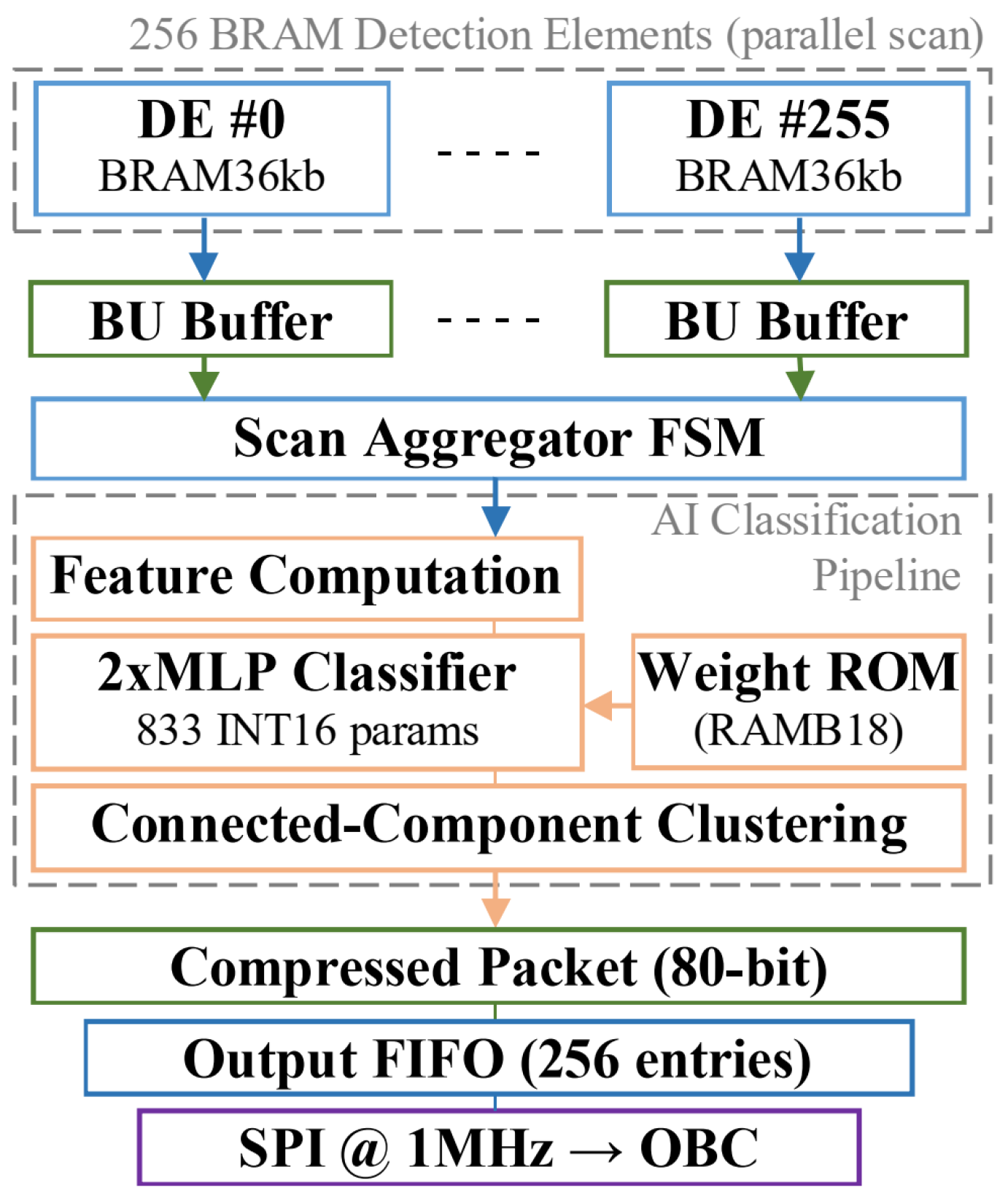
The AI-enabled Cosmic Radiation Sensor (AICoRS) is an FPGA-based radiation monitoring instrument designed for nanosatellite platforms [9]. The system is implemented on an AMD Artix-7 XC7A200T device (28 nm, speed grade −2 L) and consists of two principal subsystems: a SEU Detector Matrix (SDM) and a control and communication back-end. A hosting PCB implementation targeting a 3U CubeSat form factor has been developed for this platform [29]. A block diagram of the enhanced AICoRS architecture, comprising the 256 detection-element array, the per-DE BU-buffers, the scan-aggregation finite-state machine (FSM), the classification backend (feature extraction, two MLP cores sharing one weight read-only memory (ROM), connected-component clustering), and the classified-packet output path, is shown in Figure 2.
The SDM comprises 256 DE, each realized as a single 36 Kb BRAM primitive configured in Simple Dual Port mode (2048 addresses × 18 bits). Every BRAM is initialized with a deterministic pattern—alternating 0x15555 and 0x2AAAA at even and odd addresses, respectively—ensuring a uniform spatial distribution and an equal count of ones and zeros across the 36,864 cells. A TMR-protected counter continuously loops through the address space while a monitor module compares the read-back data against the expected pattern. When a mismatch is detected, the monitor outputs the address and a bitmap of the affected bits, then corrects the stored value through the write port [9].
All 256 DE are scanned in parallel with a period of 1 ms at a 10 MHz clock frequency. Each scan cycle consists of an active phase lasting 2053 clock cycles (≈205 µs), during which the counters traverse the full address space, and a dead-time window of 7947 cycles (≈795 µs) available for post-scan processing. The 10 MHz operating frequency was selected to minimize power consumption and reduce susceptibility of the control logic to radiation-induced transients, while still providing sufficient scan throughput for expected orbital SEU rates. The resulting optimized configuration, utilizing all available BRAMs (365 BRAM36 primitives [30]), achieves a total FPGA power draw of 0.5 W, satisfying the power budget of nanosatellite-class platforms [23].
Detected BU are serialized through a priority encoder, written into a 256-entry FIFO, and transmitted to the OBC via a 1 MHz SPI link. Each BU is encapsulated in an 80-bit legacy packet containing the 11-bit address, 18-bit upset bitmap, 8-bit DE index, 16-bit scan timer, and 8 status/flag bits. No on-chip analysis, classification, or aggregation is performed prior to transmission. As a consequence, the maximum sustainable event rate is bounded by the SPI link capacity: at 80 bits per packet and a 1 MHz SPI clock, the system can transmit at most 12,500 packets per second, or approximately 12 packets within one 1 ms scan period. When the number of detected BU per scan exceeds the FIFO depth, data loss occurs—a limitation that becomes critical under high-intensity radiation conditions.

2.3. Offset-Histogram Classification

The offset-histogram method provides a statistical reference approach for MCU classification that exploits the deterministic nature of the physical-to-logical mapping [24]. The key insight is that because the bit-interleaving function within a given BRAM primitive is fixed, any pair of physically adjacent cells always maps to the same pair of logical coordinates. The logical-address difference (offset) ( Δ addr , Δ bit ) between two cells of an MCU event is therefore a characteristic signature of that physical adjacency relation under the prevailing mapping.
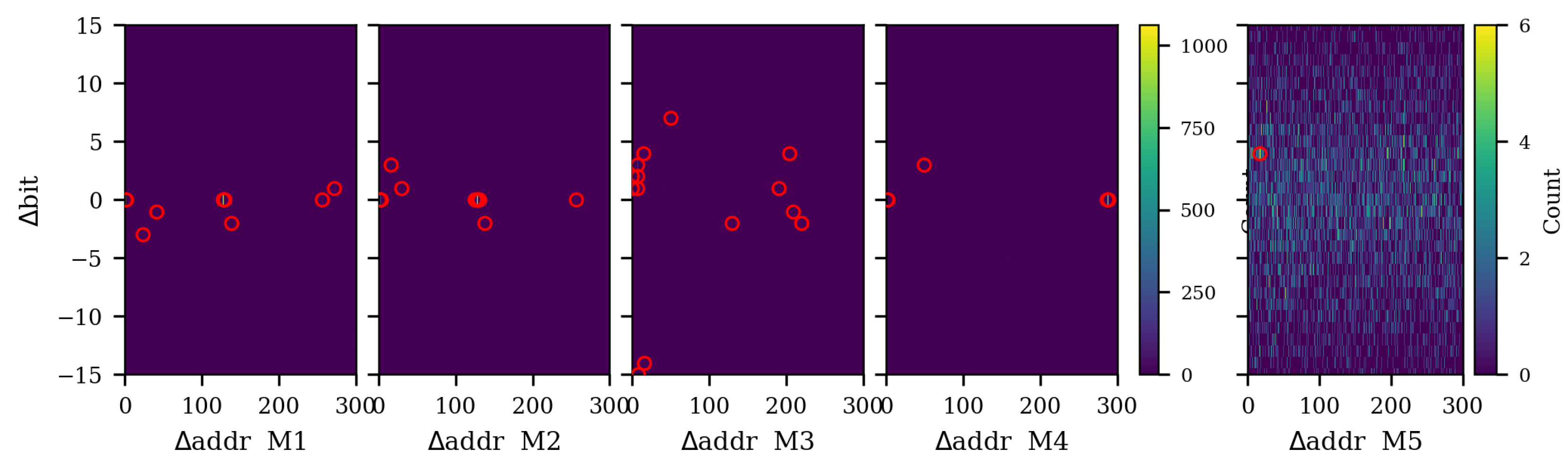
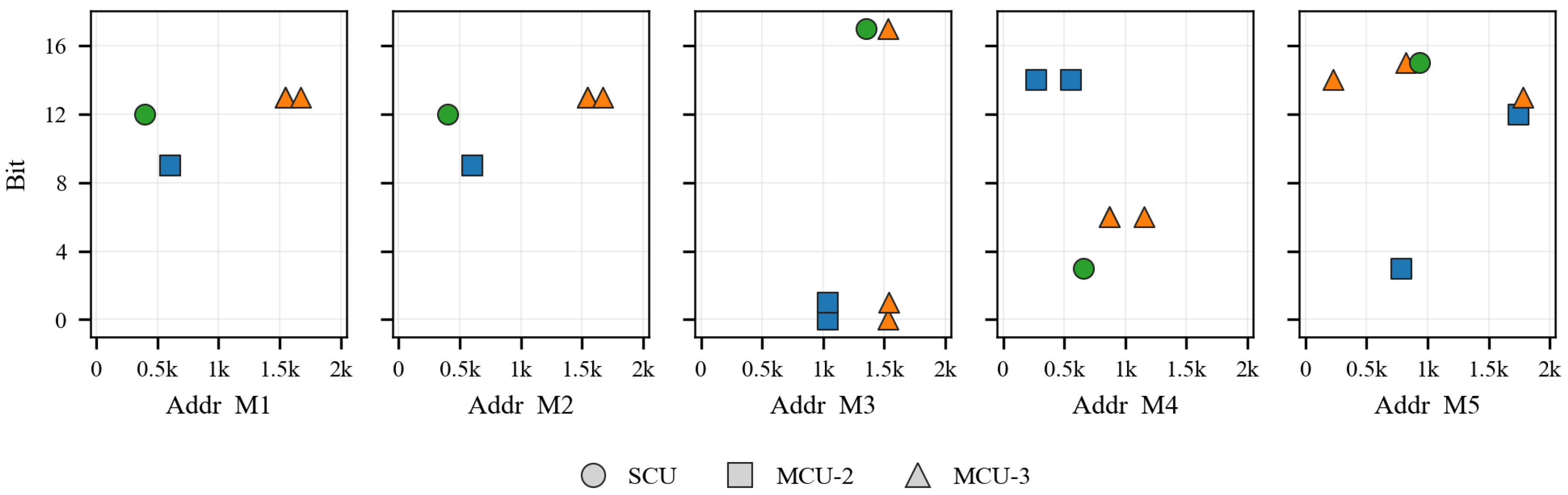
The method operates in two phases. In the calibration phase, a two-dimensional histogram of all pairwise offsets ( Δ addr , Δ bit ) is accumulated over a large number of scan cycles. Offset bins corresponding to physical adjacency relations accumulate significantly more counts than the uniform background produced by random coincidences. A robust peak detector based on the median absolute deviation (MAD) identifies bins whose z-score exceeds a configurable threshold (e.g., z > 5 ), producing an adjacency list—a compact set of offset signatures that characterize the MCU fingerprint of the mapping. In the classification phase, each pair of BU detected within a single scan is tested against the adjacency list: if the observed offset matches a listed entry, the pair is labeled as MCU; otherwise, the pair is labeled as independent SCU. Connected-component analysis is then applied to the pairwise labels to recover MCU clusters. The pairwise offset histograms produced by the calibration phase are shown in Figure 3: structured mappings M1–M4 exhibit a small number of sharp peaks corresponding to physical-neighbor signatures, while the random-permutation mapping M5 produces a flat, structureless distribution that defeats peak detection. This concentration of multiple-cell upsets into a few dominant offset signatures, rather than a uniform distribution, is consistent with irradiation-based analyses of 28 nm Xilinx FPGAs: for the Kintex-7 configuration memory, the offsets ( 1 , 1 ) , ( 0 , 1 ) , ( 1 , 1 ) and ( 1 , 0 ) were identified as the high-probability physical-adjacency signatures under heavy-ion irradiation [24], with the same set—extended by ( 0 , 2 ) and ( 1 , 2 ) —reported independently for a 28 nm device in [31]. This qualitative agreement supports the physical plausibility of the structured synthetic mappings; it does not, however, constitute validation of the proprietary Artix-7 BRAM geometry, which would require a dedicated irradiation campaign.
The offset-histogram method achieves near-perfect classification when calibrated, as demonstrated in Section 6. The adjacency list is extremely compact—typically up to 18 entries—and can be stored in a small ROM or LUT, enabling single-cycle classification of each upset pair on an FPGA.
Importantly, the method is topology-invariant: it automatically discovers the relevant offset peaks from the statistical accumulation of pairwise offsets, without requiring prior knowledge of the physical interleaving layout. However, the method has a critical operational limitation, hereafter referred to as the cold-start problem. Constructing the adjacency list requires that a sufficient body of MCU events has already been collected—typically several thousand scan cycles at a heavy-ion or proton beam facility (e.g., CHARM/CERN, TAMU, or PSI). Before this calibration is complete, the peak detector has no statistical basis for distinguishing MCU signatures from the uniform coincidence background, and the classifier produces no usable output (F1 = 0). Moreover, because the adjacency list encodes the proprietary physical-to-logical mapping of a specific die, it cannot be transferred between devices: each FPGA chip or silicon revision requires an independent calibration campaign. This cold-start limitation motivates the machine-learning approach developed in Section 3, which aims to provide a deployable classifier that functions from first power-on without chip-specific calibration data.

3. Proposed Method

The proposed architecture comprises three components: a synthetic data generation framework (Section 3.1), an MLP classifier for pairwise SCU/MCU classification (Section 3.2), and a classified telemetry format with per-DE aggregation (Section 3.3).

3.1. Synthetic Data Generation

Because the physical bit-interleaving layout of AMD/Xilinx BRAM primitives is proprietary and not documented publicly, training a supervised classifier requires synthetic data with known ground-truth labels. The data generation framework decouples the physics of particle interactions from the chip-specific address mapping, enabling the same underlying radiation scenario to be projected through multiple hypothetical layouts.
In other papers, like [32,33], SEUs are also modeled as simple bit upsets randomly injected in the sequential elements of a design. Even the AMD Soft Error Mitigation core [21] includes optional error-injection features. Furthermore, in real irradiation experiments, there is no 100% certainty that several BUs form an MCU or SEUs, even if they match an adjacency model.

3.1.1. Physical Memory Model

Each 36 Kb BRAM primitive is modeled as a two-dimensional physical array of 288 × 128 = 36,864 cells, matching the actual capacity of a BRAM36 configured as 2048 × 18 (Simple Dual Port). The aspect ratio 288:128 ≈ 2.25:1 is consistent with the physical proportions of BRAM columns observed in the Vivado Device View (≈150 µm × 50 µm).

3.1.2. SEU Event Model

Radiation events are generated in two stages. In the first stage (physics), the number of SEU events per scan cycle is drawn from a Poisson distribution with rate parameter λ . Each event is classified as either SCU (probability 1 P MCU ) or MCU (probability P MCU ). SCU events are placed uniformly at random on the physical array. MCU events are modeled as clusters of 2–4 physically adjacent cells: MCU-2 comprises a horizontal or vertical pair, MCU-3 a three-cell line or L-shape, and MCU-4 a 2 × 2 square. The empirical multiplicity distribution reported for 28 nm SRAM technologies indicates that MCU-2 events account for approximately 85–90% of MCU events, MCU-3 events for 6–7%, MCU-4 events for 3–5%, and MCU-5+ events for no more than 1% under moderate-LET heavy-ion irradiation [24,31]. In the proposed synthetic training set, the multiplicity distribution was set to P ( MCU - 2 ) = 0.85 , P ( MCU - 3 ) = 0.12 , and P ( MCU - 4 ) = 0.03 , while MCU-5+ events were not included due to their very low reported occurrence. This distribution preserves the empirical dominance of two-cell clusters while moderately oversampling three-cell clusters to improve their representation during supervised training. For 16 nm UltraScale+ FinFET devices, the distribution is shifted towards smaller cluster sizes due to the reduced cross-section and tighter cell pitch [27]. Each shape is randomly rotated by 0 , 90 , 180 , or 270 to increase diversity. Boundary conditions use wrap-around (modular) arithmetic to avoid edge artifacts that would arise from clamping.

3.1.3. Physical-to-Logical Mapping

In the second stage (mapping), the physical coordinates of all events are transformed to the logical address space ( a d d r , b i t ) through five bijective mapping functions, each representing a plausible bit-interleaving scheme:
  • M1—Linear (bit-major):  k = bit × 2048 + addr , row-major unfolding. Adjacent physical columns map to consecutive addresses.
  • M2—Address-interleaved: Identical to M1, except that for odd bit indices the address order is reversed. This models a simple interleaving strategy intended to separate adjacent bits across ECC words.
  • M3—Linear (address-major):  k = addr × 18 + bit , row-major. Bits within the same word are physically adjacent—the layout is most vulnerable to within-word MBU.
  • M4—Column-major:  k = bit × 2048 + addr , with column-major unfolding. Physical neighbors can yield address offsets of ±288, the largest among the structured mappings.
  • M5—Random permutation: A fixed random bijection ( seed = 2026 ), representing the worst-case scenario in which no structural pattern exists between physical and logical coordinates.
We expect commercial SRAMs to employ regular repeating patterns of physical to logical mapping. A complete random mapping might create large timing differences between nets. Nevertheless, we included this mapping as a worst-case scenario.
The algebraic expression k ( addr , bit ) is identical for M1 and M4, but the two mappings differ in how the linear index k [ 0 , 36 , 863 ] is unfolded into the physical 288 × 128 grid. M1 uses row-major unfolding, so ( row , col ) = ( k / 128 , k mod 128 ) and adjacent physical columns differ by Δ k = 1 , i.e., Δ addr = 1 . M4 uses column-major unfolding, so ( row , col ) = ( k mod 288 , k / 288 ) and adjacent physical rows differ by Δ k = 1 while adjacent physical columns differ by Δ k = 288 —this is what produces the ± 288 neighbor-offset signature visible in Figure 3 (M4).
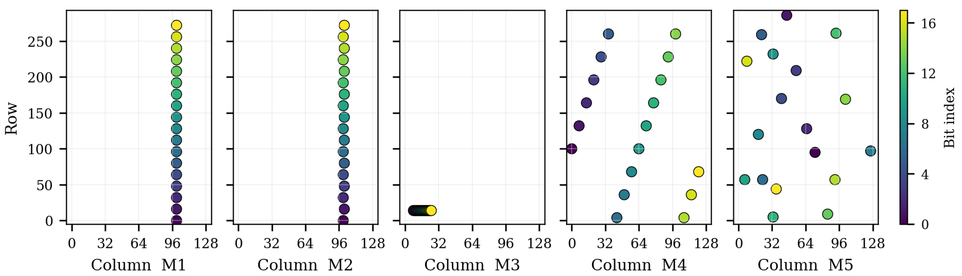
Applying all five mappings to the same set of physical events guarantees that differences in classifier performance across mappings are attributable solely to the mapping geometry and not to random variation in the underlying radiation scenario. The distribution of detected upsets in physical (row, column) coordinates for each of the five mappings is shown in Figure 4; the corresponding scan outputs in logical (address, bit) coordinates, obtained from the same underlying radiation scenario, are illustrated in Figure 5.

3.1.4. Pair Formation

Within each scan cycle containing k 2 detected BU, all k 2 ordered pairs ( i , j ) with i < j (sorted by address) are formed, subject to the filter | Δ addr | 300 . This threshold was chosen to encompass the largest MCU offset signature observed across all structured mappings: mapping M4 produces physical-neighbor offsets of ±288, so a margin of 300 ensures complete coverage while limiting the combinatorial cost. Each pair is assigned a ground-truth label: y = 1 if both BU originate from the same particle event MCU, and y = 0 otherwise (independent SCU or coincident events from different particles).

3.1.5. Correspondence to Empirical SEU Statistics

The generator parameters used throughout the paper ( λ = 2.0 SEU/scan, P MCU = 0.10 , multiplicity distribution as defined above) balance physical plausibility with statistical efficiency. The value λ = 2.0 does not represent an on-orbit upset rate: per-bit SEU cross-sections span roughly six orders of magnitude between the atmospheric-neutron regime ( 6.32 × 10 15  cm2/bit for Artix-7 BRAM [11]) and heavy-ion saturation ( 7.94 × 10 9  cm2/bit [12]), and, for quiet low-Earth-orbit conditions, the expected number of upsets per 1 ms scan cycle of the 9.4  Mb array is several orders of magnitude below unity. Instead, λ = 2.0 is a deliberately accelerated rate that guarantees each simulated scan cycle contributes multi-upset coincidences to the training and evaluation statistics. The classifier itself operates on per-pair geometric features (Equation (1)) that do not depend on the absolute event rate; the rate-dependent quantity—the proportion of coincident SCU pairs among all candidate pairs—is explicitly characterized by the λ sweep of the sensitivity analysis (Section 6.2). The selected MCU fraction P MCU = 0.10 and the cluster-size sub-distribution match the proton- and heavy-ion-induced statistics reported for the same technology node [24]; for 16 nm UltraScale+ FinFET devices the distribution is shifted towards smaller cluster sizes due to the reduced cross-section and tighter cell pitch [27]. The sensitivity analysis characterizes classifier robustness across a 20× range of λ and a 4× range of P MCU around these values.

3.2. MLP Classifier

3.2.1. Architecture and Input Features

The classifier is a three-layer Multi-Layer Perceptron [34] with architecture 8 32 16 1 . The hidden layers use ReLU activations and are preceded by batch normalization; the output layer produces a scalar probability via the sigmoid function. Dropout is applied during training at rates of 0.2 and 0.1 for the first and second hidden layers, respectively.
The MLP was selected over more expressive architectures (e.g., DeepSets [35], graph neural networks [36]) on the basis of three practical considerations for FPGA deployment. First, the pairwise formulation reduces the input to a fixed 8-element vector, eliminating the need to handle variable-sized inputs. Second, the MLP has a fixed and predictable resource cost on the FPGA regardless of the mapping complexity, whereas a lookup-table baseline grows with the number of distinct adjacency offsets (which is unknown a priori for a real chip). Third, the MLP weights can be updated via a new bitstream without register-transfer-level (RTL) modifications, enabling recalibration after beam testing of a specific chip (see Section 3.2.3 below).
The eight input features for each upset pair ( i , j ) are:
x = a i 2047 , b i 17 , a j 2047 , b j 17 , | Δ a | 2047 , | Δ b | 17 , Δ a 2047 2 , Δ b 17 2
where a i , a j [ 0 , 2047 ] are logical addresses, b i , b j [ 0 , 17 ] are bit positions, and Δ a = a j a i , Δ b = b j b i . Features 5–6 are the normalized absolute address/bit offsets (direct analogues of the offset-histogram signatures), while features 7–8 introduce nonlinear sensitivity to the inter-pair distance.

3.2.2. Training Procedure

The network is trained using the Adam optimizer with an initial learning rate of 10 3 and a batch size of 512. The loss function is binary cross-entropy with logits (BCEWithLogitsLoss), with a positive-class weight w + = N neg / N pos to compensate for the class imbalance (MCU pairs constitute approximately 10–15% of the dataset). A weighted random sampler further balances the classes within each mini-batch. Training proceeds for up to 100 epochs with early stopping based on validation F1 (patience = 15 epochs), and the learning rate is reduced on plateau via ReduceLROnPlateau.
For FPGA deployment, the batch-normalization layers are analytically folded into the preceding linear weights and biases:
W = γ σ 2 + ϵ · W , b = γ σ 2 + ϵ · ( b μ ) + β
where γ , β , μ , σ 2 are the learned BatchNorm parameters and ϵ = 10 5 . This transformation absorbs the BatchNorm scale/shift parameters ( γ , β ) into the preceding linear weights and discards the running statistics ( μ , σ 2 ) needed only during training, reducing the parameter count from 929 to 833. The folded weights are then quantized to 16-bit signed fixed-point (Q8.8 format: 8 integer bits, 8 fractional bits) by scaling each floating-point value by 256, rounding, and clipping to the range [ 32 , 768 , + 32 , 767 ] . Fixed-point INT16 quantization has been shown to preserve the accuracy of compact MLP models within fractions of a percentage point relative to their FP32 baseline [37], while halving memory footprint and enabling deterministic single-cycle multiply-accumulate operations on FPGA digital signal processor (DSP) slices [38]. The resulting 833 INT16 parameters occupy 1.66 KB and fit within a single RAMB18E1 block.
During training, the output probability is obtained as σ ( z ) > 0.5 , where σ denotes the sigmoid function and z is the pre-activation logit produced by the final linear layer. Because the sigmoid is monotonically increasing with σ ( 0 ) = 0.5 , the decision rule σ ( z ) > 0.5 is mathematically equivalent to z > 0 . The FPGA implementation exploits this equivalence by evaluating only the sign of the accumulated logit, eliminating the need for any sigmoid computation—whether via a lookup table, piecewise-linear approximation, or floating-point arithmetic—at the decision boundary.

3.2.3. Deployment Pipeline

The deployment workflow for a specific FPGA chip admits two operating modes. In the default calibration-free mode, the MLP is trained exclusively on synthetic data covering the five representative bit-interleaving layouts (Section 3.1), and the resulting weight ROM is embedded in the bitstream uploaded to the satellite—no chip-specific data are required, and classification is available from the first scan cycle on any Artix-7 device. If chip-specific beam-test data become available (optional refinement path), the same RTL can be redeployed with retrained weights as follows: (1) the chip is exposed to heavy-ion irradiation at a beam-test facility to collect ground-truth MCU/SCU data from a single BRAM primitive (the interleaving pattern is identical across all BRAM primitives on the same die, so one BRAM suffices for calibration); (2) the MLP is retrained on the collected data using the procedure described above; (3) a Python 3.14 script performs BatchNorm folding, Q8.8 quantization, and generates the Verilog weight ROM file (mlp_weights.v); (4) the weight ROM is programmed into the FPGA. Steps (2)–(4) require only the 833 INT16 weight values to be updated; the RTL logic is unchanged. In practice, the new weights are embedded into the FPGA bitstream generated by Vivado, and the complete bitstream is uploaded to the satellite. The architecture therefore supports both calibration-free first-flight deployment and post-flight accuracy refinement through the same weight-ROM update mechanism.

3.3. Classified Telemetry Format

In the baseline AICoRS architecture [9,23], each detected BU generates one 80-bit SPI packet. At a 1 MHz SPI clock, the link can transmit at most 12 legacy packets per scan. When the SEU rate exceeds this threshold the 256-entry FIFO overflows and data are lost. This limitation becomes critical under accelerator qualification conditions or during elevated orbital radiation environments (Section 6).

3.3.1. Classified Packet Format

The enhanced architecture produces a single 80-bit classified summary packet for each active detection element on every scan cycle. Bit [72] of the packet header is set to 0, distinguishing the classified format from the baseline legacy format (bit [72] = 1) and simultaneously serving as a radiation-alarm flag visible to the OBC. While the baseline architecture detects only generic bit upsets (BUs), the MLP-based classification step further distinguishes them into single-cell (SCU) and multiple-cell (MCU) categories. The classified packet contains the DE index, the total BU count, the number of classified SCU and MCU clusters in the current scan, and the size of the largest MCU cluster. The detailed bitfield layout is specified in Section 5. Because both formats share the same 80-bit frame size and SPI physical layer, the OBC identifies the format by reading bit [72].
The MLP classifier runs unconditionally on every scan cycle—there is no threshold-based mode switching—and FIFO-overflow elimination is a direct consequence of the reduced packet count (one packet per active DE instead of one per BU).

3.3.2. Clustering and Per-Element Aggregation

The complete classification-and-aggregation pipeline—pairwise MLP inference, connected-component clustering of MCU labels, and packing of per-DE statistics into a single 80-bit SPI frame—is shown schematically in Figure 6. The MLP classifier processes all upset pairs within each active detection element. The pairwise classification results are assembled into an adjacency graph in which each BU is a vertex and an edge connects any pair classified as MCU ( P > 0.5 ). A connected-component algorithm then partitions the graph: isolated vertices (degree 0) are counted as SCU events, while connected components of size ≥ 2 are counted as MCU clusters. The per-element summary (N_BU, N_SCU, N_MCU, max_cluster_size) is packed into a single 80-bit classified frame.
Each detection element stores up to four BU positions (address and bit index) in a 16-bit-per-entry buffer that is filled in parallel with the scan phase, adding zero latency overhead. For a DE with k BU, the number of pairs to classify is k 2 : at most 6 pairs for k = 4 , which is processed by two parallel MLP cores in approximately 2670 cycles (≈267 µs at 10 MHz). Should the BU count in a given DE exceed the buffer depth—an extreme scenario not encountered in simulation—the aggregator falls back to reporting only the raw BU count without MLP classification.

4. Experimental Setup

This section specifies the parameters of the synthetic data, the metrics used to assess classification quality, the six experiments conducted, and the FPGA implementation flow targeting the Artix-7 200T device. The same data pipeline is reused across all experiments so that performance differences reflect classifier architecture rather than sampling variation.

4.1. Data Generation Parameters

Synthetic datasets were generated using the framework described in Section 3.1 with the parameters summarized in Table 1. A total of 10,000 scan cycles were simulated per mapping, yielding 20,026 SEU (18,022 SCU and 2004 MCU across all multiplicity classes). The Poisson mean λ = 2.0 is a deliberately accelerated event rate adopted for statistical efficiency rather than an estimate of the on-orbit upset rate (see Section 3.1), while P ( MCU ) = 0.10 reflects the empirically observed MCU fraction in 28 nm FPGA technologies [24].
The 80/20 train–test split was applied at the scan level: the first 8000 scans served as the training set (used for both the offset-histogram calibration and MLP training), while the remaining 2000 scans formed the held-out test set. Upset pairs were formed from all scans containing k 2  BU, yielding k 2 candidate pairs per scan filtered by | Δ addr | 300 .

4.2. Evaluation Metrics

Classification quality is assessed using four standard metrics [39] computed on the held-out test pairs: accuracy, precision, recall, and F1 score. Of these, recall is the most operationally significant metric for space applications: a missed MCU event (false negative) means that a multi-cell upset goes undetected and could silently compromise ECC protection, whereas a false alarm (false positive) merely inflates the MCU count in the telemetry without affecting onboard data integrity. The F1 score is adopted as the primary ranking metric because it balances precision and recall in a single figure of merit. The false-positive rate (FPR) is reported as a complementary measure of SCU misclassification.

4.3. Experiments

Six experiments were designed and conducted in order to evaluate different aspects of the proposed system:
Experiment 1—Per-mapping classification. For each of the five mappings (M1–M5), a separate MLP model is trained and tested on data from that mapping alone (80/20 split). The offset-histogram baseline is evaluated on the same splits. This experiment measures the attainable classification quality when the physical bit-interleaving layout is known and the classifier is calibrated for a specific chip.
Experiment 2—Cross-mapping generalization. A single MLP model is trained on mappings M1–M3, validated on M4 (column-major, unseen during training), and tested on M5 (random permutation, maximally dissimilar). This experiment quantifies the extent to which features learned from one set of structured layouts transfer to unseen geometries—a practical scenario for initial deployment before chip-specific calibration.
Experiment 3—FIFO overflow simulation. The per-DE classified telemetry format (Section 3.3) is evaluated over a range of SEU intensities λ [ 2 , 200 ] , with 1000 scans simulated per λ value (the choice of upper bound is justified in Section 6). For each scan cycle, the legacy (1 packet/BU) and classified (1 packet/DE) packet counts are compared against the 256-entry FIFO depth to determine the overflow rate. This experiment is independent of the classification method and characterizes the data-loss reduction achieved by per-DE aggregation alone.
Experiment 4—Sensitivity analysis. To assess whether the MLP performance reported in Experiments 1–2 is robust to the choice of data-generation parameters, a one-at-a-time sweep is performed across three axes: (i) the Poisson SEU rate λ { 0.5 , 1.0 , 2.0 , 5.0 , 10.0 } , (ii) the MCU probability P MCU { 0.05 , 0.10 , 0.20 } , and (iii) the MCU cluster-size distribution (full mix 85/12/3% vs. MCU-2 only). For each of the eight resulting configurations, the full data-generation and training pipeline is re-executed with five independent random seeds. Every seed repeats Experiments 1, 2, and the held-out variant (trained on M1–M2, validated on M3, tested on M4 and M5), providing three complementary views of classifier robustness. F1 is reported as mean ± std across seeds.
Experiment 5—Feature ablation. To determine the contribution of each feature group, the eight MLP input features are partitioned into three semantic groups: absolute coordinates ( f 0 f 3 : normalized addr and bit positions of each BU), linear offsets ( f 4 f 5 : | Δ addr | , | Δ bit | ), and squared offsets ( f 6 f 7 : ( Δ addr ) 2 , ( Δ bit ) 2 ). Four feature-set configurations are evaluated: Full (all 8), Config A (6 features, squares removed), Config B (6 features, linear offsets removed), and Config C (4 features, coordinates removed). Each configuration is tested on all three MLP evaluation protocols (per-mapping, cross-mapping, held-out) using the baseline data ( λ = 2.0 , P MCU = 0.10 , full mix).
Experiment 6—Alternative classifier comparison. To contextualize the reference MLP selection, four additional classifier architectures are trained using the same data pipeline and evaluated under the three protocols above: a decision tree (DT, depth 8), a linear SVM (9 parameters), a compact MLP (8 → 16 → 1, 161 parameters), and an enlarged MLP (8 → 64 → 32 → 1, 2689 parameters). All five architectures are subsequently implemented in synthesizable Verilog and taken through post-implementation in Vivado 2024.1 on the Artix-7 200T, so that classification accuracy can be compared against FPGA resource cost on a unified basis.
FPGA implementation. Three design configurations—the Baseline (the original, previously published AICoRS design [9,23], without on-chip classification), the Histogram classifier, and the MLP classifier—were taken through the full Vivado 2024.1 implementation flow targeting the Artix-7 200T (−2 L speed grade, SBG484 package). Synthesis employed the Flow_AlternateRoutability strategy with LUT combining suppressed (-directive NoCombineLuts); these settings were required to close routing at the >90% LUT fill levels characteristic of both classified configurations. Post-implementation utilization, timing, and power reports were generated using the Vivado Power Analyzer tool and serve as the reference for all FPGA results reported in Section 5. In [23], we measured the power draw of the FPGA chip configured with a similar design and concluded that the tool estimation matches closely with the measurements.
Statistical methodology. Each stochastic MLP configuration was evaluated over five training runs using distinct random seeds (seeds 1–5), affecting weight initialization, mini-batch ordering, and the train/validation split, while all other experimental parameters were held fixed. Where aggregate statistics are reported, the mean across the five runs is given together with the Bessel-corrected sample standard deviation as the measure of run-to-run variability. For the held-out M4 evaluation, the 95% confidence interval of the mean F1 score was calculated using Student’s t-distribution ( n = 5 ).

5. FPGA Implementation

This section describes how the proposed classification backend is integrated with the existing AICoRS hardware, how the MLP and offset-histogram classifiers are realized in synthesizable Verilog, and how the three reference designs (Baseline, Histogram, MLP) compare in post-implementation utilization, timing, and power. The dead-time budget at the end establishes the operational margin that any future classifier extension must preserve.

5.1. Integration Strategy

The enhanced proposed AICoRS architecture was integrated into the existing AICoRS Vivado project with minimal modification to the original design. A scan-aggregation module replaces the original priority encoder: it accepts the 256-wide BU-ready signal bus from the detector array and, during the 7947-cycle dead-time window between successive scans, drives the classification backend with upset pairs from each active detection element, accumulates per-element classification counts, and assembles the classified summary packets. The classification backend is interchangeable: either the two parallel MLP cores (Section 5.2) or the offset-histogram lookup (Section 5.3) can be instantiated, sharing the same BU-buffer infrastructure and aggregation pipeline. The 256 detection-element instances, the PLL, and all peripheral IP blocks were left unchanged.

5.2. MLP Forward Pass on FPGA

The MLP classifier implements the architecture 8 → 32 → 16 → 1 with ReLU activations on the hidden layers. The inference datapath uses the folded INT16 weights described in Section 3.2.2, stored in a single RAMB18E1 block.
Arithmetic is performed in fixed-point Q8.8 format (INT16, 16-bit signed), which allows all multiply-accumulate (MAC) operations to be mapped onto a single DSP48E1 primitive operating sequentially. The forward pass for one upset pair proceeds as follows: the 8-element input vector is normalized by pre-stored scale factors. Division by 2047 (address) and 17 (bit-index) is implemented as reciprocal multiplication using precomputed Q8.8 constants, eliminating the need for a divider IP block; three DSP48E1 slices are time-shared between the two cores for these operations (3 DSP cycles per feature), then the three-layer computations are serialized through the shared MAC unit. The total latency is approximately 890 clock cycles per pair at 10 MHz (≈89 µs). Two identical MLP cores share the weight ROM and operate in parallel to halve the per-scan processing time.
The binary classification decision reduces to a sign check on the final accumulator (Section 3.2.2); no sigmoid hardware (LUT, piecewise-linear, or floating-point) is therefore required.

5.3. Offset-Histogram Classifier on FPGA

The offset-histogram method described in Section 2.3 was also implemented on the FPGA as an alternative classification backend, sharing the same BU-buffer infrastructure and per-DE aggregation pipeline as the MLP variant. The FPGA implementation realizes only the classification phase of the algorithm: the computationally intensive calibration phase (histogram accumulation, MAD-based peak detection, adjacency-list extraction) is performed offline on a ground station, and the resulting adjacency list is loaded into the FPGA as a pre-computed lookup table.
The hardware consists of four functional blocks. First, a small distributed ROM stores the adjacency list—typically 10–18 entries, each comprising a ( Δ addr , Δ bit ) pair encoded as a 16-bit word (10 bits for address offset, 6 bits for bit offset). Second, an offset calculator computes the signed difference ( Δ a , Δ b ) between each pair of BU coordinates using two subtractors. Third, a comparator array tests the computed offset against every entry in the adjacency list; this can be implemented as a fully parallel array (≈288 LUT, single-cycle latency) or as a sequential scanner (≈30 LUT, 1–18 cycles per pair). Fourth, connected-component logic groups pairwise MCU labels into clusters, identical to the logic used by the MLP variant.
The total resource footprint of the histogram classifier itself is estimated at ≈100–500 LUT, 0 DSP48E1, and 0 BRAM tiles—negligible compared to the BU-buffer overhead that dominates both classified variants. The classification latency is 1 clock cycle per pair (parallel comparator) or up to 18 cycles per pair (sequential comparator); even in the sequential configuration, the 14 pairs expected at λ = 200 complete in ≈720 cycles (≈72 µs at 10 MHz), safely within the 7947-cycle dead-time budget.
The key operational constraint of this implementation is that the adjacency ROM contents must match the actual physical BRAM layout of the specific FPGA device. A new chip or silicon revision requires a fresh calibration campaign at an accelerator facility to re-derive the adjacency list. This topology dependence is the fundamental trade-off relative to the MLP classifier, which operates without chip-specific calibration data.

5.4. Classified Telemetry—Hardware Bitfield

The 80-bit classified packet uses the following bitfield layout: DE_index[8], N_BU[8], N_SCU[8], N_MCU[8], max_size[4], reserved[16], type[4], timer[16], flags[8].
Bit [72] serves as the format indicator: a value of 0 identifies a classified per-DE summary, while a value of 1 denotes a legacy per-BU packet (retained in the RTL for diagnostic use). This single-bit flag simultaneously provides the OBC with cycle-by-cycle radiation-environment awareness without additional signaling bandwidth.

5.5. Resource Utilization

Using the implementation flow described in Section 4, all three designs were taken through synthesis and place-and-route to generate post-implementation reports. Table 2 compares resource usage across the baseline, offset-histogram, and MLP-enhanced designs.
The per-DE BU-buffer infrastructure—four 16-bit entries and a find-first-one priority encoder instantiated in each of the 256 detection elements—is responsible for the bulk of the resource increase. The total LUT increment over the Baseline is 40,923 LUTs for the Histogram design and 42,618 LUTs for the MLP design (Table 2); the post-synthesis hierarchical utilization report attributes ≈85% of this increment, in both cases, to the replicated per-DE buffer logic rather than to the classifier datapath. The classifier datapath itself contributes a comparatively minor fraction. The offset-histogram classifier itself requires only a small adjacency ROM, offset calculator, and comparator array (Section 5.3), contributing negligible resources relative to the buffer infrastructure. The MLP classifier—two parallel cores sharing one weight ROM—contributes fewer than 3000 LUTs, one RAMB18E1, and five DSP48E1 slices, distributed as follows: one MAC unit per MLP core (two total) and three for feature normalization (address scaling, bit-index scaling, and squaring), shared between both cores. The BRAM and DSP overheads are therefore negligible in absolute terms.

5.6. Timing and Power

Table 3 summarizes the post-implementation timing results. All three designs meet the 10 MHz clock constraint (100 ns period) with ample margin. The worst-case setup slack ranges from +26.132 ns (baseline) to +26.970 ns (MLP); in all three cases the critical path is the debug hub Test Clock (TCK) (33 ns period), not the main 10 MHz clock. The reported worst negative slack is bounded by the 33 ns debug-hub TCK domain; on the 100 ns main-clock (clk_out1) domain the slack is substantially larger, so the design retains a wide timing margin at the 10 MHz operating point and is not the limiting factor for any classifier variant.
All power figures reported in this section are post-implementation vectorless estimates from the Vivado Power Analyzer at typical process corner and nominal supply voltages; physical measurement on hardware has not yet been performed. Table 4 reports the on-chip power consumption estimated under these conditions. Both classified variants consume approximately 0.124–0.127 W more than the baseline, an increase of 17–18%. The additional dynamic power is distributed between routing and switching logic. DSP and BRAM components contribute less than 1 mW of additional power. The MLP variant consumes 3 mW less than the histogram variant. Within the MLP variant, the MLP cores and feature-extraction logic together contribute only ∼5 mW—approximately 0.6% of the total on-chip power. The 3 mW gap between the two classified variants (0.836 W vs. 0.839 W) is therefore within the estimation noise, indicating effectively identical thermal profiles. Two important caveats apply to these figures: vectorless analysis uses default toggle rates rather than activity from real workloads, so actual switching activity at runtime may be lower (particularly during the inter-scan dead-time when most of the design is idle); and the typical process corner used by Vivado is a midpoint estimate, with a ±15–20% spread across silicon parts due to process variation. Hardware measurement on the deployment chip is therefore required for final power characterization, as also noted in the Discussion (Section 6).

5.7. Dead-Time Budget

Within the 7947-cycle dead-time window between successive scans (Section 2.2), the MLP processing must complete before the next scan begins. Table 5 quantifies the budget under representative operating conditions.
Even under the most demanding tested scenario ( λ = 200 SEU/scan), the two parallel MLP cores complete all ≈14 upset-pair classifications within ≈6400 cycles, leaving a margin of 1547 cycles (155 µs) before the next scan begins. This headroom is sufficient to accommodate moderate increases in event multiplicity or future expansion of the classifier without affecting the 1 ms scan period. If the available dead-time budget is exceeded—an extreme scenario not observed in simulation—the same fallback path described in Section 3.3 suppresses MLP classification for that scan, ensuring transmission is never delayed.

6. Experimental Results and Discussion

The experimental results are organized as follows: classification performance under per-mapping and cross-mapping protocols is presented first, followed by the sensitivity and ablation analyses, the FIFO-overflow characterization, the consolidated three-way FPGA comparison, and the alternative-classifier evaluation. A unified discussion of the operational implications concludes the section.

6.1. Classification Performance

Table 6 presents the classification metrics for the offset-histogram baseline and the MLP classifier across all five synthetic BRAM physical mapping configurations. The offset-histogram method achieves near-perfect F1 scores (0.996–0.997) for the four structured mappings (M1–M4), because these layouts produce repeatable, stable offset distributions that are reliably captured by the histogram peak detector. For mapping M5 (random permutation), the baseline yields F1 = 0.000: no consistent offset pattern exists, so the peak detector produces random output.
Unless a table indicates otherwise, the MLP F1 values reported in this section are means across five independent training seeds; where dispersion is shown it is the Bessel-corrected sample standard deviation, and 95% confidence intervals are reported for the held-out M4 evaluation. The per-mapping and cross-mapping results (Table 6), the sensitivity (Section 6.2), ablation (Section 6.3), and alternative-classifier (Section 6.6) studies were conducted as independent training campaigns with separate random-seed pools; consequently, the reference-MLP figures may differ by a few percentage points between Table 6 and the later ablation and alternative-classifier studies, while the qualitative ordering of configurations remains stable. The MLP classifier trained and tested on the same mapping (per-mapping experiment) achieves F1 scores of 0.922–0.971 for M1–M4, lagging the baseline by 2.6–7.5 percentage points. A notable property shared by all four structured mappings is that the MLP produces almost no false negatives (mean Recall ≥ 0.998): nearly every MCU event is correctly identified, and the modest precision losses (FPR 2.3–6.0%) reflect conservative classification that labels borderline pairs as MCU rather than missing them. This asymmetric error profile is beneficial for space applications, where an undetected MCU (false negative) is more costly than a spurious alarm (false positive). For mapping M5, the MLP attains F1 = 0.1785, which—while modest—represents the only non-zero result in the random-mapping scenario.
In the cross-mapping experiment (MLP trained on M1–M3, evaluated on the two withheld layouts), the classifier attains F1 = 0.739 on the unseen column-major mapping M4, driven by near-perfect recall (0.996) at a precision of 0.588 (FPR = 0.272). The precision penalty arises because a fraction of coincident SCU pairs exhibit offset signatures that overlap with genuine MCU patterns learned from the training set. On M5 (random permutation), F1 drops to 0.128: the absence of any shared offset structure between training and test layouts leaves the classifier with no transferable discriminative information (Recall = 0.220, FPR = 0.278).
These per-mapping and cross-mapping results illustrate the complementary roles of the two classifiers. When calibrated on the target chip, the offset-histogram method is unambiguously superior (F1 > 0.99). The MLP addresses the cold-start regime defined in Section 2.3: it provides a non-trivial classification baseline from the first scan cycle—accepting a lower accuracy ceiling in exchange for immediate availability without chip-specific data. The sensitivity analysis in the following subsections quantifies how this baseline behaves under varying radiation parameters.
The classification results presented here are based on synthetic data; the design has not been validated on real hardware under irradiation conditions.

6.2. Sensitivity to Data-Generation Parameters

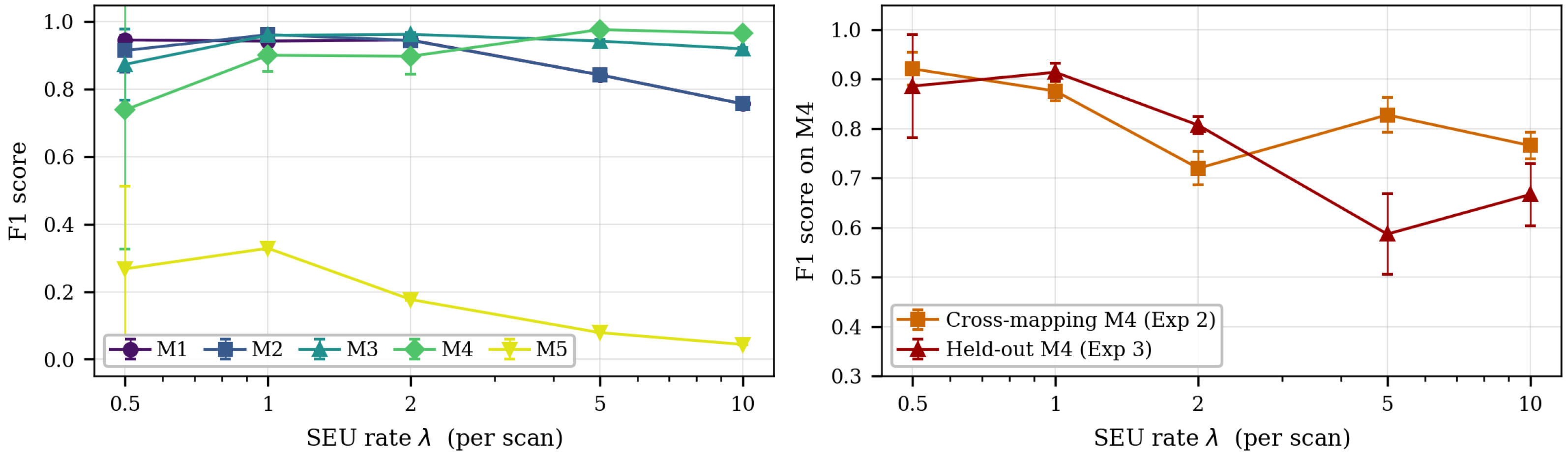
The classification results reported above were obtained with a single set of data-generation parameters ( λ = 2.0 , P MCU = 0.10 , full MCU-size mix). To assess whether these results are an artifact of that specific configuration, a one-at-a-time sensitivity sweep was conducted: each parameter was varied independently while the remaining two were held at their baseline values, and the full training–evaluation pipeline was repeated for five independent random seeds per configuration. Each seed executed three MLP evaluation protocols: per-mapping training (Experiment 1), cross-mapping generalization trained on M1–M3 with M4 as validation target (Experiment 2), and a stricter held-out variant trained on M1–M2 only, validated on M3, with M4 as primary test and M5 as adversarial test. The λ sweep results are reported in Table 7 and summarized graphically in Figure 7; Table 8 presents the P MCU and MCU-size sweeps, and Table 9 reports the held-out generalization results.
SEU rate ( λ ). The per-mapping F1 scores for the structured mappings (M1–M4) remain above 0.84 (mean) across the entire 20× range of λ values tested (0.5–10.0), confirming that the MLP is not sensitive to the overall event density. Two trends are visible. First, at high λ (5.0, 10.0), F1 on M1 and M2 decreases from ≈0.95 to ≈0.76: the elevated number of coincident SCU events per scan produces a higher rate of false-positive pairs whose offsets overlap with genuine MCU signatures, reducing precision. In contrast, M3 and M4 are less affected (F1 > 0.92 at λ = 10 ) because their physical structures produce more distinctive offset patterns. Second, at low λ (0.5), the training set is substantially smaller (only 11.9% of scans contain ≥2 BU, compared to 62.5% at λ = 2.0 ), which increases training variance across seeds (e.g., M4 std = 0.41) but does not degrade the best-seed performance.
The cross-mapping and held-out results (Table 7 and Table 9) reveal two additional findings. First, both generalization metrics improve at low λ : cross-mapping M4 F1 reaches 0.92 at λ = 0.5 versus 0.72 at λ = 2.0 , and held-out M4 F1 reaches 0.89 versus 0.81, because fewer coincident SCU pairs reduce the false-positive rate. Second, the held-out protocol (trained on only two mappings) is more sensitive to high- λ noise than the cross-mapping protocol: at λ = 5.0 , held-out M4 F1 drops to 0.587 while cross-mapping M4 F1 remains at 0.828. Training on three mappings provides sufficient structural diversity to absorb the increased noise, whereas two mappings do not. At moderate intensities ( λ 2.0 ), the two protocols yield comparable results, and the held-out variant even exceeds the cross-mapping score at λ = 1.0 (0.914 vs. 0.876), suggesting that the smaller but more homogeneous training set (M1–M2) can produce a less overfitted model under favorable signal-to-noise conditions.
MCU fraction ( P MCU ). Increasing P MCU from 0.05 to 0.20 monotonically improves per-mapping, cross-mapping, and held-out F1 across all configurations. At P MCU = 0.20 , the per-mapping F1 on all four structured mappings exceeds 0.958, and the held-out M4 F1 reaches 0.881. This trend is expected: a higher MCU fraction provides more positive training examples, improving the class balance and enabling the MLP to learn MCU offset signatures with greater precision. At P MCU = 0.05 , per-mapping F1 decreases by approximately 5 pp on average, cross-mapping M4 F1 drops to 0.611, and held-out M4 F1 to 0.710—all still substantially above the chance level of a random classifier.
MCU cluster-size distribution. Restricting the training data to MCU-2 events only (100%/0%/0%) has minimal impact on per-mapping F1 (within 0.5 pp of the baseline full mix). The generalization metrics show a consistent but moderate penalty: cross-mapping M4 F1 decreases from 0.720 to 0.636 (−8.4 pp), and held-out M4 F1 from 0.807 to 0.741 (−6.6 pp). This indicates that the diversity of offset patterns provided by MCU-3 and MCU-4 clusters contributes to cross-layout generalization, though the effect is modest since MCU-2 already dominates the full mix (85%).

6.3. Feature Ablation

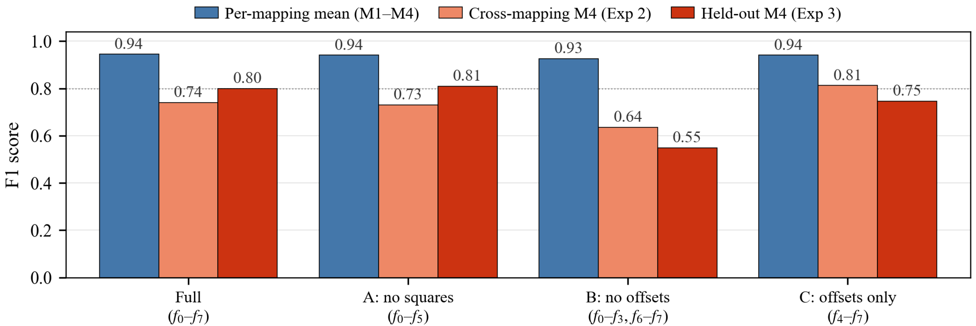
To determine which of the eight MLP input features carry the discriminative information and whether the feature set can be reduced for a more efficient FPGA implementation, a systematic ablation study was conducted. Four configurations were evaluated: Full (all 8 features), Config A (6 features, squared offsets f 6 f 7 removed), Config B (6 features, linear offsets f 4 f 5 removed), and Config C (4 features, absolute coordinates f 0 f 3 removed, retaining only the offset-derived features f 4 f 7 ). Each configuration was evaluated using Experiments 1, 2, and the held-out protocol; the hidden-layer architecture (32/16) and all hyperparameters were held constant, with only the input dimensionality changed. The numerical results are reported in Table 10, and a graphical summary of the held-out F1 across all four configurations is provided in Figure 8.
Three findings emerge. First, removing the squared offset features (Config A) is harmless: across all three evaluation protocols the change relative to the Full configuration is statistically insignificant. Per-mapping F1 changes by at most 1.1 pp on M1–M4, cross-mapping M4 F1 by −0.9 pp, and held-out M4 F1 by +1.1 pp (from 0.800 to 0.810), well within the overlapping 95% confidence intervals ( [ 0.745 , 0.854 ] vs. [ 0.791 , 0.829 ] ). This indicates that the ReLU-based hidden layers can learn the necessary nonlinear distance sensitivity from the linear offsets alone, so that the pre-computed squared features carry no additional discriminative information. On the FPGA, eliminating f 6 and f 7 would remove two 16-bit multiplications from the scan_aggregator module, saving approximately 64 LUTs and 2 DSP48E1 cycles per pair without degrading generalization to unseen layouts.
Second, removing the linear offsets while retaining coordinates and squares (Config B) produces the only substantial degradation observed in the study: M2 per-mapping F1 drops by 4.5 pp, and held-out M4 F1 drops by 25.0 pp (from 0.800 to 0.549), with M4 recall collapsing well below the near-perfect levels of the other configurations—the only configuration in which the MLP fails to detect a significant fraction of MCU events. The squared features f 6 , f 7 contain the same magnitude information as f 4 , f 5 but in a compressed nonlinear form that discards the sign and reduces dynamic range for small offsets, making them an inadequate substitute. Linear offsets are therefore the most critical feature group.
Third, reducing the feature set to offsets only (Config C, 4 features) preserves per-mapping performance almost exactly (all Δ within ±0.9 pp for M1–M4) and even improves cross-mapping M4 F1 by 7.3 pp. The held-out M4 F1 decreases by 5.4 pp (from 0.800 to 0.746), indicating that absolute coordinates provide a modest benefit for generalization when the training set is small (two mappings), but are not essential. This result confirms that the MLP learns an offset-based decision boundary analogous to the histogram method, with the coordinates serving as auxiliary regularization rather than primary discriminative features.

6.4. FIFO Overflow Elimination

The packet-level behavior of the two telemetry formats was evaluated over the full tested range λ [ 2 , 200 ] SEU/scan (Poisson-distributed), with the numerical results summarized in Table 11. The upper bound λ = 200 represents an accelerator qualification intensity (e.g., CHARM/CERN, TAMU, LANSCE) rather than an orbital scenario: typical LEO upset rates are λ 1 per scan, and even GEO peaks during solar particle events reach only λ 10 per scan. Validating the design at this extreme intensity provides margin for environments beyond nominal LEO–South Atlantic Anomaly core passages, extreme solar particle events, and potential future missions in higher-radiation orbits.
For the legacy format the average packet count grows proportionally to the number of detected BU events, reaching 239.9 packets at λ = 200 and thereby exceeding the FIFO depth of 256 in a fraction of scan cycles. The classified telemetry format aggregates all upsets within a detection element into a single 80-bit summary, reducing the count to 148.9 packets at λ = 200 —a 38% reduction (1.61× compression ratio), sufficient to keep all scans within the FIFO capacity. The compression ratio grows from 1.08 at λ = 2 to 1.61 at λ = 200 , while the legacy FIFO overflow rate jumps from 0% to 19.4% at the highest tested intensity. The classified format maintains a 0% overflow rate at every tested intensity.
A radiation monitoring instrument must not silently lose data under extreme conditions—precisely when the radiation environment carries the greatest scientific and operational significance. The operational consequence is asymmetric: under the baseline architecture, dropped events are silent—the OBC has no indication that data have been lost. The classified telemetry format avoids this failure mode by design: each DE reports its BU count, SCU/MCU classification, and maximum cluster size on every scan cycle, even though per-event addresses are not transmitted. This constitutes graceful degradation (observation at reduced resolution) rather than silent data loss (complete blindness).

6.5. Three-Way FPGA Comparison

Table 12 consolidates the key performance and resource figures for all three configurations. The histogram and MLP variants occupy 122,376 and 124,071 Slice LUTs, respectively—an increment of 40.9 k and 42.6 k over the baseline. As established in Section 5, the per-DE BU-buffer infrastructure is responsible for the vast majority of this growth; the classifier-specific datapath contributes fewer than 3000 LUTs and 5 DSP48E1 slices in the MLP case and negligible additional logic in the histogram case. The Vivado power analyzer reports 0.839 W and 0.836 W for the histogram and MLP variants—a 3 mW difference that falls within the estimator’s noise floor. All three configurations achieve timing closure at 10 MHz with ample margin (WNS > +26 ns).
Both classified variants eliminate FIFO overflow at λ = 200 by aggregating per-element statistics into a single 80-bit classified frame. The offset-histogram classifier achieves near-perfect accuracy (F1 > 0.99) on calibrated structured mappings, while the MLP achieves F1 = 0.922–0.971 on the same mappings and provides the unique advantage of calibration-free operation in the cold-start regime.

6.6. Alternative Classifier Evaluation

Experiment 6 extends the FPGA evaluation to four additional classifier architectures implemented in Verilog and taken through the complete Vivado 2024.1 synthesis and place-and-route flow targeting the same Artix-7 200T device: a decision tree (DT, depth 8, 63 nodes, Experiment 3 training split), a linear SVM (9 parameters), a compact MLP (8 → 16 → 1, 161 parameters), and an enlarged MLP (8 → 64 → 32 → 1, 2689 parameters). All five classifiers—including the reference MLP (8 → 32 → 16 → 1, 833 parameters)—were implemented within the same base design (256 DE array, scan_aggregator) so that resource differences reflect classifier cost only. Table 13 consolidates classification accuracy and post-implementation FPGA resources for all five classifiers. Note that the reference-MLP figures in Table 13 (124,666 LUT) differ slightly from those in Table 2 (124,071 LUT) because the two implementation runs were generated in separate Vivado sessions targeting different design comparisons (three-way Baseline/Histogram/MLP vs. five-way classifier sweep): the underlying RTL of the reference MLP is identical, but place-and-route seeding produces minor variations of order 0.5% in absolute LUT count.
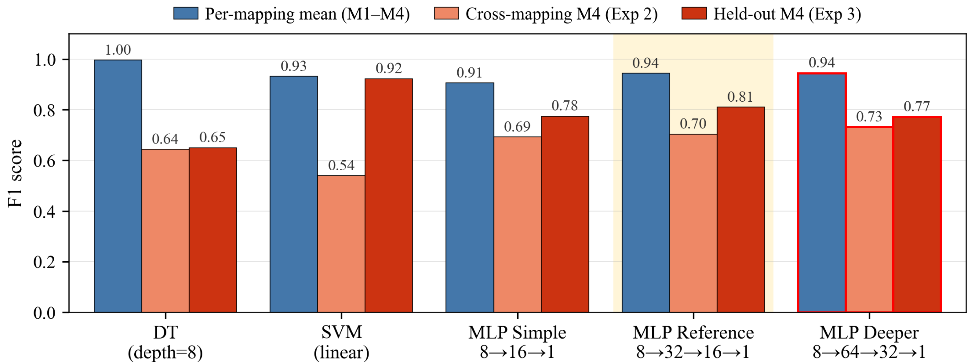
The F1 score of all five classifiers under the three evaluation protocols is summarized in Figure 9; the reference MLP is the only architecture, among those evaluated, that simultaneously satisfies all four operational constraints (highest held-out F1 without an identified structural artifact, high recall, successful timing closure, and an incremental classifier-specific cost of 1981 LUTs, corresponding to approximately 1.5% of the device LUT capacity, although the complete design remains highly utilized).
Per-mapping accuracy (calibrated ceiling). The per-mapping F1 values reported in this paragraph correspond to the calibrated-ceiling regime (Experiment 1: training and testing on the same mapping). They are presented for completeness and as an upper reference; the operational performance of the deployed AICoRS classifier is given by the held-out F1 numbers in the next paragraph. The decision tree achieves the highest per-mapping F1 on structured mappings (0.994–0.997 on M1–M4), substantially outperforming all MLP variants. This is expected: a depth-8 tree with up to 131 leaf nodes has sufficient capacity to memorize the finite set of MCU offset patterns for a specific mapping, functioning as a lookup table. The MLP architectures (8 → 16 → 1 through 8 → 64 → 32 → 1) achieve nearly identical per-mapping F1 (0.91–0.97), with no significant differentiation as a function of parameter count.
Cross-mapping generalization. The picture reverses completely under the held-out evaluation protocol (trained on M1–M2, validated on M3, tested on M4 and M5; held-out protocol, Section 4, Experiment 4). The DT collapses to F1 = 0.650, Recall = 0.487—it memorizes training-mapping patterns and does not generalize, missing every second MCU event on an unseen layout. The linear SVM achieves a nominally high held-out F1 = 0.922 on M4; however, this is a structural artifact: M1, M2, and M4 share similar bit-major offset symmetries, so the linear boundary trained on M1–M2 transfers directly to M4, while failing completely on mappings with different structure (cross-mapping M4 F1 = 0.540). The result, therefore, does not constitute cross-mapping generalization in the general sense. Among the MLP-based classifiers, the reference MLP (8 → 32 → 16 → 1) achieves the highest mean held-out M4 F1 score of 0.810 (95% CI: 0.788–0.833), with near-perfect mean recall. The compact MLP (8 → 16 → 1) achieves a mean F1 score of 0.775 (95% CI: 0.666–0.885). The enlarged MLP (8 → 64 → 32 → 1) does not improve the mean held-out performance despite a 3.2× increase in parameter count, achieving a mean F1 score of 0.772 (95% CI: 0.724–0.821). It also exhibits greater run-to-run variability than the reference MLP, indicating that the additional model capacity provides no measurable benefit under the tested cross-mapping protocol.
FPGA resource comparison. The Δ LUT overhead relative to the DT design (which represents the shared infrastructure cost) ranges from +845 LUT for the SVM to +4050 LUT for the enlarged MLP. Crucially, even the largest gap—1136 additional LUTs between SVM and reference MLP—corresponds to less than 0.9% of device capacity, confirming that the choice among these classifiers is not a hardware-cost decision. The decisive FPGA result is the timing closure failure of the MLP 8 → 64 → 32 → 1 design: at 94.2% LUT utilization, place-and-route cannot satisfy hold constraints for the synchronous BRAM-based weight ROM, producing 118,647 failing endpoints (WHS = −0.427 ns). This design cannot be deployed. The reference MLP, by contrast, achieves timing closure with WNS = +27.41 ns—the same order of margin as the much simpler DT and SVM designs.
Summary. The reference MLP (8 → 32 → 16 → 1) is the optimal classifier: it achieves the highest held-out cross-mapping F1 among all tested architectures, maintains near-perfect recall (near-zero missed MCU events), meets timing closure with ample margin, and does so at a resource increment of only 1981 additional LUTs (+1.5% of device capacity) over the DT baseline. No tested alternative simultaneously satisfies all four criteria.

6.7. Discussion

The central finding of this work is the three-way post-implementation comparison on the Artix-7 200T (Table 2, Table 3, Table 4, Table 5, Table 6, Table 7, Table 8, Table 9, Table 10, Table 11 and Table 12): the dominant cost of on-chip classification is the shared BU-buffer and aggregation infrastructure (Section 5), not the classifier datapath. The total LUT overhead of the MLP variant (+42,618 LUT, +31.7%) is dominated by the BU-buffer infrastructure, with the classifier datapath itself contributing only a small fraction. This concentration of resource cost in the BU-buffer is a deliberate architectural choice motivated by three considerations: (i) the parallel scan of 256 BRAM detectors within a single 205 µs active window requires local per-DE buffering, since a centralized buffer would demand a 256-bit-wide bus or time-multiplexing at unacceptable throughput cost; (ii) per-DE buffers isolate failure modes, ensuring that a fault in one detection element cannot compromise the rest of the array; and (iii) the architecture scales linearly with detector count—each additional DE costs approximately 165 LUT—which yields predictable resource scaling when porting to higher-density devices. At 92.2% LUT utilization, the MLP design meets all timing constraints (WNS = +26.97 ns, WHS = +51 ps) after place-and-route with the Flow_AlternateRoutability strategy and NoCombineLuts directive (Section 4); this is an operationally valid configuration for the 256-DE target, with the practical implication that further scaling to 1024+ DE requires migration to a higher-density device rather than architectural rework.
Three concrete optimization paths exist for future implementations to reduce the LUT footprint. First, the BU-buffer depth can be reduced from four entries to two: under the modeled multiplicity distribution, per-DE occupancies exceeding two BU within a single scan cycle are rare at orbital event rates, so a depth-2 buffer preserves the pair statistics while halving the dominant replicated storage cost. Second, the ffo18 logic can be moved from individual detector elements to a shared arbiter, eliminating replication across 256 instances. Third, the system can be ported to a higher-density UltraScale+ device: the 16 nm UltraScale+ BRAM heavy-ion saturation cross-section is approximately 4× smaller per bit ( 2 × 10 9  cm2/bit, [10]) compared to the 28 nm generation ( 7.94 × 10 9  cm2/bit, [12]), which directly reduces the required number of detector elements for a given sensitivity target and proportionally lowers both LUT and power overhead. A fourth path is suggested by the feature ablation study (Section 6.3): the squared-offset features ( f 6 , f 7 ) can be removed without any classification degradation (the held-out F1 change lies within the 95% confidence interval), eliminating two 16-bit multiplications per pair in the feature-extraction datapath. Combined with a reduction from 8 to 6 input features, this simplifies the first MLP layer from 8 × 32 = 256 to 6 × 32 = 192 multiply-accumulate operations, yielding a modest but cumulative saving in both logic and latency.
A further consideration for orbital deployment is the radiation susceptibility of the classifier weights themselves. The 833 INT16 parameters stored in the RAMB18E1 weight ROM (13,328 bits in total) are subject to the same SEU mechanisms as the detector array, and a single bit flip in a high-magnitude weight could shift the classification boundary and degrade accuracy. Quantitatively, however, the weight ROM constitutes a small target: its 13,328 bits represent roughly 0.14% of the 9.4 × 10 6 bits of the detector array, so, irrespective of the radiation environment and the applicable per-bit cross-section, its expected SEU rate is nearly three orders of magnitude lower than that of the array itself. Furthermore, the Q8.8 fixed-point encoding produces a strongly bit-position-dependent sensitivity: the magnitude of the perturbation caused by a single bit flip grows exponentially with bit position, from ± 2 8 ± 0.004 for the least-significant fractional bit to ± 128 for the most-significant magnitude bit, so upsets in the high-order bits constitute the operationally relevant failure mode. This bit-position-dependent sensitivity is consistent with fault-injection studies on FPGA-based neural-network accelerators, which mitigate weight and control-register upsets through selective triple modular redundancy of critical bits, weight limiting, and error-correction coding of control-state registers [32,33]; in the present pairwise MLP, the final-layer weights and logic are the most influential for the classification outcome. Three complementary mitigation strategies are available without significant architectural changes: (i) remapping the weight memory to a RAMB36E1-based 64-bit simple-dual-port organization would make the primitive’s native single-error-correction, double-error-detection (SEC-DED) circuitry available. This would replace the current RAMB18E1 with one RAMB36E1, corresponding to one additional 18-Kb BRAM equivalent. The required 64/72-bit data packing and ECC-parity initialization or loading would need to be implemented separately; single-bit errors would be corrected on read, while persistent errors would still require reloading or scrubbing; (ii) periodic verification and restoration of the weight memory from a protected golden copy, either through a dedicated user-logic access path to the BRAM or by reconfiguration through the ICAP interface, with the refresh interval selected according to the estimated weight-memory upset rate; the AMD Soft Error Mitigation (SEM) controller protects the configuration memory and does not, on its own, correct the contents of user BRAM at runtime; and (iii) triple modular redundancy of the weight ROM (+2 RAMB18E1, raising BRAM utilization from 72.6% to 72.9%) enables continuous detection and correction of weight upsets with negligible resource overhead. These approaches are complementary rather than mutually exclusive: ECC protects against single-bit corruption per access, scrubbing prevents accumulation of latent multi-bit errors, and TMR provides the strongest guarantee against high-energy multi-cell upsets within the weight ROM itself, at the cost of more than 200% overhead in terms of area and power compared to a single processing unit [40]. Recent surveys confirm that the radiation robustness of on-board machine-learning models remains an open research area [41]; the implementation and evaluation of these mitigation strategies on the proposed system is identified as a concrete direction for future work.
The power increase from baseline to either classifier (+0.124–0.127 W) is moderate and is dominated by the increased routing switching activity rather than the BRAM or DSP additions. At the 10 MHz operating frequency selected for radiation tolerance [9], the total on-chip power of both classified variants (0.836–0.839 W) is within the thermal budget established in prior characterization work [23]. For reference, a 3U CubeSat with body-mounted solar panels typically operates with a power budget of 7–20 W [42], placing the AICoRS draw at 4–12% of the platform budget. For platforms requiring tighter power constraints, reducing the BU-buffer depth and increasing the scan period (thereby lowering dynamic activity) are the most effective levers.
The classification results confirm a fundamental trade-off between the two classifiers, characterized by four operating points: (a) without prior calibration, the offset-histogram method has an empty adjacency list and produces F1 = 0; (b) the MLP in calibration-free deployment achieves a mean held-out M4 F1 of 0.807 ± 0.017 (95% CI [0.786, 0.828], five seeds; Table 9) on the unseen column-major layout M4 with near-perfect recall (held-out protocol, Section 4); (c) when chip-specific data are available, the same MLP architecture reaches F1 = 0.92–0.97 per mapping (Experiment 1); and (d) the histogram method, once calibrated, achieves F1 > 0.99. Therefore, the MLP does not replace the histogram in calibrated scenarios; rather, it extends the system’s operational capability to the cold-start regime—initial deployment, new chip revisions, or missions without prior beam-test access—where the histogram produces no usable output. In this sense the MLP provides a non-zero classification floor from first power-on; under chip-specific calibration the same architecture approaches, although does not fully reach, the calibrated histogram ceiling (F1 = 0.92–0.97 vs. F1 > 0.99). The near-perfect recall observed across structured layouts (mean Rec ≥ 0.998) is operationally desirable for radiation monitoring, where under-reporting MCU events is more harmful to environmental characterization than over-reporting them. The sensitivity analysis (Section 6.2) reinforces this finding for the calibration-free deployment regime: across the 20× λ sweep and the 4× P MCU sweep, the cross-mapping F1 on unseen M4 remains above 0.61 and the stricter held-out protocol (trained on only two mappings) maintains M4 F1 above 0.59 even in the most challenging λ = 5.0 configuration.
The architecture also supports a smooth transition from calibration-free to chip-specific deployment via the optional refinement path described in Section 3. When chip-specific beam-test data become available, retraining is expected to recover the per-mapping F1 ceiling, with an absolute improvement of approximately Δ F1 ≈ +0.11–0.16 over the cold-start floor (0.81 → 0.92–0.97 on the relevant mapping). Crucially, this refinement does not require any RTL changes: only the 833 INT16 weights stored in the ROM are updated through the Python conversion pipeline (Section 3), and the regenerated bitstream is uploaded over the existing telecommand channel. This deployment-pipeline invariance enables a single hardware design to address both first-flight cold-start operation and post-flight refinement; quantitative validation of the expected improvement on real beam-test data is itself identified as a target for future work.
The alternative classifier evaluation (Section 6.6) provides a broader empirical context for the reference MLP selection. The key finding is that resource cost is not the differentiating factor: the Δ LUT range between the cheapest viable classifier (SVM, +845 LUT) and the reference MLP (+1981 LUT) is only 1136 LUT—less than 0.9% of device capacity. The decisive differentiation is in cross-mapping robustness. The memorization-based DT achieves near-perfect per-mapping accuracy but fails in cross-mapping scenarios (Recall = 0.487), while the linear SVM achieves high Exp3 F1 on M4 only because of structural symmetry between training and test mappings, not general feature learning. The enlarged MLP (8 → 64 → 32 → 1) further demonstrates that the FPGA resource budget for classifiers is not unbounded: beyond ≈93–94% LUT utilization, routing closure cannot be guaranteed, and the design fails with hold violations. This establishes a practical upper bound on classifier complexity for this device and operating point. Taken together, these results position the reference MLP as the architecture that best balances classification generalizability, implementation reliability, and parameter efficiency within the constraints of the target FPGA platform.
Beyond the per-pair classification accuracy reported above, cluster-level reconstruction of higher-order events (MCU-3 and MCU-4) deserves separate consideration. Recovering an MCU-k cluster does not require all k 2 pairwise labels to be correct: because clusters are formed by connected-component analysis, a spanning subset of k 1 correctly identified adjacency pairs is sufficient to group the cluster, and the iterative bridging procedure tolerates a fraction of misclassified pairs. Per-pair errors nevertheless reduce the probability of recovering the full cluster, and this sensitivity grows with k. Under chip-specific calibration this effect is small for both classifiers; in the calibration-free regime, however, MCU-3 and especially MCU-4 events may be under-reported or fragmented into smaller predicted clusters. The operational impact of this effect is bounded by the rarity of large clusters: at moderate LET, MCU-3 and MCU-4 events together represent only a few percent of total SEU events in 28 nm technologies [24] (their fraction rises at high LET and grazing incidence [31]), so the on-board computer is expected to interpret the N_MCU and max_MCU_size telemetry fields with awareness of this caveat under uncalibrated operation. A targeted experimental quantification of this effect, together with a multi-class MLP that classifies clusters of size k { 1 , 2 , 3 , 4 } directly rather than composing them from pairwise decisions, is identified as future work.
Several limitations of the present study should be acknowledged explicitly. First, all classification results are based on synthetic data with modeled bit-interleaving layouts. This methodological choice is necessitated by the proprietary nature of the physical bit-interleaving in Xilinx BRAM [28], which makes direct comparison between simulated and real silicon geometry impossible without a chip-specific beam-test campaign; nonetheless, the five layouts M1–M5 are designed to bracket the geometric complexity expected on real devices (Section 3.1), and the sensitivity analysis (Section 6.2) demonstrates that classification performance is not tuned to a specific parameter choice. Second, the random-permutation layout M5 represents an intentional worst-case stress test rather than a realistic mapping for commercial FPGA devices: silicon vendors deliberately structure bit-interleaving to optimize ECC efficiency, and a fully random permutation is neither economically nor architecturally plausible. The cross-mapping F1 of approximately 0.13 on M5 should therefore be interpreted as a pessimistic lower bound, not as a representative deployment result, because it combines the absence of learnable offset structure with the exclusion of some true MCU pairs by the | Δ addr | 300 candidate window. Third, the synthetic data generator models MCU multiplicities in the range 2–4, consistent with empirical observations at 28 nm technology nodes, where two-cell clusters dominate the MCU population and clusters of five or more cells account for no more than ∼1% of MCU events [24]; larger or geometrically more complex clusters—for example, elongated multi-cell tracks produced by grazing-incidence ions—are not represented in the training set. Because the MLP classifies pairs rather than entire clusters, larger clusters predominantly decompose into the same dominant neighbor-adjacency offsets observed for smaller MCUs [24,31] rather than into qualitatively new signatures; the expected failure mode is therefore fragmentation of such clusters into smaller reported clusters rather than a complete loss of detection. The parametric synthetic data generator allows the training distribution to be extended without architectural change, so any future empirical evidence of non-modeled cluster geometries can be incorporated by retraining alone. Fourth, the 92.2% LUT utilization of the MLP design (90.9% for the histogram variant) leaves limited headroom for additional on-chip functionality and constrains scalability on the same device; concrete paths for both reducing the footprint on this device and migrating to higher-density platforms have been outlined earlier in this Discussion. Final validation on a physical Artix-7 200T device under irradiation at a facility such as CHARM/CERN, PSI or TAMU remains the decisive next step, and is identified as the primary item of future work.


7. Conclusions and Future Work

In this paper, we present an enhanced AICoRS architecture that advances the Baseline design through the integration of on-chip classification (Histogram and MLP variants) and per-detection-element telemetry aggregation. The contribution is sixfold: three engineering items (i–iii) and three analytical studies (iv–vi). Engineering: (i) per-DE aggregation eliminating FIFO overflow; (ii) an offset-histogram classifier achieving F1 > 0.99 on calibrated layouts; (iii) a calibration-free MLP classifier (8 → 32 → 16 → 1, 833 INT16 parameters) providing non-zero cross-mapping capability from first power-on. Analytical: (iv) a sensitivity analysis confirming robustness across a 20 × range of SEU rates and a 4 × range of MCU fractions; (v) a feature ablation study identifying squared-offset features as redundant; (vi) a comparative evaluation of four alternative classifier architectures confirming the reference MLP as the optimal choice. Detailed numerical results supporting each contribution are reported in Section 6.1, Section 6.2, Section 6.3, Section 6.4, Section 6.5 and Section 6.6.
Post-implementation resource and timing data (Table 2, Table 3, Table 4, Table 5, Table 6, Table 7, Table 8, Table 9, Table 10, Table 11 and Table 12) reveal that the inter-classifier hardware overhead is marginal compared with the shared aggregation infrastructure. The alternative classifier evaluation (Section 6.6) reinforces this finding: even architectures differing by a factor of 3.2 × in parameter count produce comparable FPGA footprints, whereas their cross-mapping robustness diverges substantially—establishing the choice between classifiers as a mission-driven decision.
Building on the contributions and limitations of this paper, four complementary directions for future work are identified and presented in the following paragraphs.

7.1. Hardware Validation

Validation on a physical Artix-7 200T device under realistic radiation conditions remains the decisive next step. A beam-test campaign at a heavy-ion or proton facility such as CHARM/CERN, PSI, or TAMU would characterize the actual physical bit-interleaving pattern of the deployed chip, generate ground-truth labeled MCU/SCU data for per-chip classifier retraining, and verify the end-to-end classification and telemetry pipeline under intensities representative of both quiet-LEO operation and the South Atlantic Anomaly. Quantitative comparison of measured versus simulated F1 scores will close the loop on the synthetic-data methodology proposed in this work (Section 3.1).

7.2. Radiation Hardening of the Classifier

The mitigation strategies outlined in Section 6—RAMB36E1-based single-error-correction, double-error-detection (SEC-DED) ECC, periodic scrubbing of the weight memory through explicit BRAM readback, verification, and rewrite, and triple modular redundancy of the weight ROM (+2 RAMB18E1, raising BRAM utilization from 72.6% to 72.9%)—are theoretically sound but have not yet been integrated into the deployment bitstream. Future work will implement at least one of these mechanisms and quantify the residual upset rate on the weight ROM under beam-test conditions, providing the empirical basis for selecting between the three approaches according to the target mission radiation environment. Beyond the weight ROM, the same strategy will be extended to the reading and classification logic—in particular, selective ECC and/or TMR of the critical control-FSM state registers and periodic scrubbing of the MLP datapath—so that the surrounding control logic is hardened alongside the stored parameters.

7.3. Architectural Extensions

A multi-class MLP that classifies clusters of size k { 1 , 2 , 3 , 4 } directly, rather than composing them from pairwise decisions, would remove the pairwise-composition stage and could reduce cluster fragmentation caused by pairwise-classification errors. The LUT-reduction paths identified in the Discussion—buffer-depth reduction, arbiter centralization, and ablation-informed removal of the redundant squared-offset features (the latter combining a minor feature-extraction change with retraining of the six-input configuration already characterized in the ablation study)—are expected to reduce the current overhead while preserving classification quality, with the largest gains anticipated from the first two paths, which target the replicated buffer infrastructure that dominates the resource cost. Domain-adaptation techniques and larger multi-mapping training sets are expected to improve cross-mapping generalization beyond the levels reported in Section 6; the sensitivity analysis (Section 6.2) indicates that even modest increases in the number of training mappings substantially improve robustness at high event rates. The broader context of on-board AI for spaceborne instrumentation [43] motivates this direction.

7.4. Power Characterization

Prior measurements on a similar AICoRS configuration have already confirmed that the Vivado estimates closely track the measured power draw [23], so no dedicated estimator-validation campaign is required. However, since the hardware-validation campaign outlined above will operate the complete classifier configurations under realistic scan activity, it will also enable direct measurement of the actual power draw of the deployed design, replacing the vectorless estimates of Section 5 with measured values and establishing the operational power envelope of the AICoRS classifier.

Author Contributions

Conceptualization, A.K., S.P., and M.I.; methodology, A.K., S.P., and M.I.; software, A.K., S.P., and A.B.; validation, A.K. and S.P.; formal analysis, A.B.; investigation, A.K.; data curation, A.K. and A.B.; writing—original draft preparation, A.K.; writing—review and editing, A.K., S.P., and M.I.; visualization, A.K. and A.B.; supervision, S.P. and M.I.; project administration, M.I.; funding acquisition, M.I. All authors have read and agreed to the published version of the manuscript.

Funding

This research was funded by the Romanian Ministry of Research, Innovation and Digitalization, project PN-IV-P8-8.3-ROMD-2023-0068 entitled “Artificial Intelligence-enabled Hardware Cosmic Radiation Sensor for Space Applications (AICoRS)”, contract no. 2ROMD/1 June 2024.

Data Availability Statement

The synthetic-data generation scripts, classifier training code, trained models, Xilinx Vivado implementation reports (resource utilization, timing, and power analysis), and all datasets required to reproduce the results presented in this study are openly available on Zenodo at https://doi.org/10.5281/zenodo.20665577.

Conflicts of Interest

The authors declare no conflicts of interest.

Abbreviations

The following abbreviations are used in this manuscript:
AICoRSAI-enabled Cosmic Radiation Sensor
ASICApplication-Specific Integrated Circuit
BRAMBlock Random-Access Memory
BUBit Upset
CRAMConfiguration RAM
DEDetection Element
DSPDigital Signal Processor
DTDecision Tree
ECCError-Correction Code
ESAEuropean Space Agency
FFFlip-Flop
FIFOFirst-In First-Out
FPGAField-Programmable Gate Array
FPRFalse-Positive Rate
FSMFinite-State Machine
GCRGalactic Cosmic Ray
GEOGeostationary Orbit
HDLHardware Description Language
LEOLow-Earth Orbit
LUTLook-Up Table
LUTRAMLook-Up Table RAM
MACMultiply-Accumulate
MADMedian Absolute Deviation
MBUMultiple-Bit Upset
MCUMultiple-Cell Upset
MLPMulti-Layer Perceptron
OBCOn-Board Computer
Q8.816-bit Signed Fixed-Point Format (8 integer + 8 fractional bits)
ROMRead-Only Memory
RTLRegister-Transfer Level
SAASouth Atlantic Anomaly
SCUSingle-Cell Upset
SDMSEU Detector Matrix
SEESingle-Event Effect
SEFISingle-Event Functional Interrupt
SELSingle-Event Latchup
SEPSolar Energetic Particles
SETSingle-Event Transient
SEUSingle-Event Upset
SPISerial Peripheral Interface
SVMSupport Vector Machine
TCKTest Clock (JTAG)
TIDTotal Ionizing Dose
TMRTriple Modular Redundancy
URAMUltraRAM
WHSWorst Hold Slack
WNSWorst Negative Slack
WPWSWorst Pulse-Width Slack

References

  1. Wirthlin, M. High-Reliability FPGA-Based Systems: Space, High-Energy Physics, and Beyond. Proc. IEEE 2015, 103, 379–389. [Google Scholar] [CrossRef]
  2. Zeynali, O.; Masti, D.; Nezafat, M.; Mallahzadeh, A. Study of “Radiation Effects of Nuclear High Energy Particles” on Electronic Circuits and Methods to Reduce Its Destructive Effects. J. Mod. Phys. 2011, 2, 1567–1573. [Google Scholar] [CrossRef][Green Version]
  3. Bailey, R. (Ed.) CAS—CERN Accelerator School: Power Converters—Radiation Risks and Mitigation in Electronic Systems; CERN: Geneva, Switzerland, 2014. [Google Scholar] [CrossRef]
  4. Aguiar, V.A.; Alberton, S.G.; Pereira, M.S. Radiation-induced effects on semiconductor devices: A brief review on single-event effects, their dynamics, and reliability impacts. Chips 2025, 4, 12. [Google Scholar] [CrossRef]
  5. Ruckerbauer, F.X.; Georgakos, G. Soft Error Rates in 65 nm SRAMs–Analysis of new Phenomena. In Proceedings of the 13th IEEE International On-Line Testing Symposium (IOLTS 2007), Crete, Greece, 9–11 July 2007; pp. 203–204. [Google Scholar] [CrossRef]
  6. Rao, N.P.; Desai, M.P. Neutron-induced strike: Study of multiple node charge collection in 14 nm FinFETs. arXiv 2017, arXiv:1706.03315. [Google Scholar]
  7. D’Aniello, F.; Tettamanti, M.; Shah, S.A.A.; Mattiazzo, S.; Bonaldo, S.; Vadalà, V.; Baschirotto, A. Single-Event Upset Characterization of a Shift Register in 16 nm FinFET Technology. Electronics 2025, 14, 1421. [Google Scholar] [CrossRef]
  8. Microsemi Corporation. Understanding Single Event Effects (SEEs) in FPGAs: A Backgrounder; Technical Report 55900134-0/8.11; Microsemi Corporation: Aliso Viejo, CA, USA, 2011. [Google Scholar]
  9. Popa, S.; Kazak, A.; Dinu, A.; Ivanovici, M.; Secrieru, N.; Carbune, V.; Melnic, V. Architecture and Design Choices for an AI-enabled FPGA-based Cosmic Radiation Sensor. In Proceedings of the 2024 International Symposium on Electronics and Telecommunications (ISETC), Timișoara, Romania, 7–8 November 2024; pp. 1–4. [Google Scholar] [CrossRef]
  10. Bertescu, A.; Popa, S.; Coliban, R.M. Feasibility of Nuclear Radiation Detection Using the SRAMs in AMD Spartan UltraScale+ FPGAs. In Proceedings of the International Conference on Electrical and Electronic Engineering (ICEEE 2026), Antalya, Turkey, 27–29 April 2026. [Google Scholar]
  11. AMD. Device Reliability Report (UG116). Available online: https://docs.amd.com/r/en-US/ug116/The-Reliability-Program (accessed on 6 June 2025).
  12. Weulersse, C.; Miller, F.; Carrière, T.; Mangeret, R. Prediction of proton cross sections for SEU in SRAMs and SDRAMs using the METIS engineer tool. Microelectron. Reliab. 2015, 55, 1491–1495. [Google Scholar] [CrossRef]
  13. Gadlage, M.J.; Roach, A.H.; Duncan, A.R.; Savage, M.W.; Kay, M.J. Electron-induced single-event upsets in 45-nm and 28-nm bulk CMOS SRAM-based FPGAs operating at nominal voltage. IEEE Trans. Nucl. Sci. 2015, 62, 2717–2724. [Google Scholar] [CrossRef]
  14. Tian, J.; Cao, R.; Liu, Y.; Cai, Y.; Mei, B.; Zhao, L.; Cui, S.; Lv, H.; Xue, Y. Electron-Induced Single-Event Effect in 28 nm SRAM-Based FPGA. Electronics 2024, 13, 2233. [Google Scholar] [CrossRef]
  15. Flad, L.; Leyer, M.; Nitz, F.S.; Krawutschke, T. A Comprehensive Survey of Redundancy Systems with a Focus on Triple Modular Redundancy (TMR). arXiv 2026, arXiv:2603.14411. [Google Scholar]
  16. Watanabe, N.; Watanabe, M. Triple Modular Redundancy Logic Design from High-Level Hardware Description. In Proceedings of the 2025 IEEE International Conference on Consumer Electronics (ICCE), Las Vegas, NV, USA, 11–14 January 2025; pp. 1–6. [Google Scholar] [CrossRef]
  17. Cannon, M.; Keller, A.; Wirthlin, M. Improving the Effectiveness of TMR Designs on FPGAs with SEU-Aware Incremental Placement. In Proceedings of the 2018 IEEE 26th Annual International Symposium on Field-Programmable Custom Computing Machines (FCCM), Boulder, CO, USA, 29 April–1 May 2018; pp. 141–148. [Google Scholar] [CrossRef]
  18. Lala, P. A single error correcting and double error detecting coding scheme for computer memory systems. In Proceedings of the 18th IEEE Symposium on Defect and Fault Tolerance in VLSI Systems, Boston, MA, USA, 5 November 2003; pp. 235–241. [Google Scholar] [CrossRef]
  19. Morgan, K.S.; McMurtrey, D.L.; Pratt, B.H.; Wirthlin, M.J. A Comparison of TMR with Alternative Fault-Tolerant Design Techniques for FPGAs. IEEE Trans. Nucl. Sci. 2007, 54, 2065–2072. [Google Scholar] [CrossRef]
  20. Legat, U.; Biasizzo, A.; Novak, F. SEU Recovery Mechanism for SRAM-Based FPGAs. IEEE Trans. Nucl. Sci. 2012, 59, 2562–2571. [Google Scholar] [CrossRef]
  21. AMD Inc. Soft Error Mitigation Controller LogiCORE IP Product Guide (PG036); AMD Inc.: Santa Clara, CA, USA, 2024. [Google Scholar]
  22. Jiang, S.; Liu, S.; Zheng, H.; Wang, L.; Li, T. Novel Radiation-Hardened High-Speed DFF Design Based on Redundant Filter and Typical Application Analysis. Electronics 2022, 11, 1302. [Google Scholar] [CrossRef]
  23. Popa, S.; Bertescu, A.; Furtună, C.; Kazak, A.; Ivanovici, M.; Martiniuc, A.; Carbune, V.; Melnic, V.; Secrieru, N. Power and Cross-Section Optimization for an FPGA-Based Cosmic Radiation Sensor. In Proceedings of the 2025 32nd IEEE International Conference on Electronics, Circuits and Systems (ICECS), Marrakech, Morocco, 17–19 November 2025; pp. 1–4. [Google Scholar] [CrossRef]
  24. Wirthlin, M.; Lee, D.; Swift, G.; Quinn, H. A Method and Case Study on Identifying Physically Adjacent Multiple-Cell Upsets Using 28-nm, Interleaved and SECDED-Protected Arrays. IEEE Trans. Nucl. Sci. 2014, 61, 3080–3087. [Google Scholar] [CrossRef]
  25. Kazak, A.; Bertescu, A.; Popa, S.; Ivanovici, M. AI-based Classification of Simulated Cosmic Radiation Bit Upsets into the SRAMs of a Commercial-grade FPGA. In Proceedings of the SPAICE 2026 Conference, ESA-ESTEC, Noordwijk, The Netherlands, 21–23 October 2026. [Google Scholar]
  26. Popa, S.; Bertescu, A.; Furtuna, C.; Ivanovici, M. Radiation-Tolerant Embedded Platform for Real-Time SEU Detection and Classification. IEEE Trans. Nucl. Sci. 2026; Submitted.
  27. Lee, D.S.; King, M.; Evans, W.; Cannon, M.; Pérez-Celis, A.; Anderson, J.; Wirthlin, M.; Rice, W. Single-Event Characterization of 16 nm FinFET Xilinx UltraScale+ Devices with Heavy Ion and Neutron Irradiation. In Proceedings of the 2018 IEEE Radiation Effects Data Workshop (REDW), Waikoloa, HI, USA, 16–20 July 2018; pp. 1–8. [Google Scholar] [CrossRef]
  28. AMD Inc. 7 Series FPGAs Memory Resources (UG473); AMD Inc.: Santa Clara, CA, USA, 2019. [Google Scholar]
  29. Bertescu, A.; Popa, S. The Design and Implementation of an FPGA-Based Cosmic Radiation Sensor PCB. In Proceedings of the 2025 18th International Conference on Engineering of Modern Electric Systems (EMES), Oradea, Romania, 29–30 May 2025; pp. 1–4. [Google Scholar] [CrossRef]
  30. AMD Inc. 7 Series FPGAs Data Sheet: Overview (DS180); AMD Inc.: Santa Clara, CA, USA, 2024. [Google Scholar]
  31. Gao, S.; Li, X.Y.; Zhao, S.W.; He, Z.; Ye, B.; Cai, L.; Sun, Y.M.; Xiao, G.Q.; Cai, C.; Liu, J. Heavy ion-induced MCUs in 28 nm SRAM-based FPGAs: Upset proportions, classifications, and pattern shapes. Nucl. Sci. Tech. 2022, 33, 161. [Google Scholar] [CrossRef]
  32. Cai, Y.; Cai, M.; Wu, Y.; Lu, J.; Bian, Z.; Liu, B.; Cui, S. Evaluation and Mitigation of Weight-Related Single Event Upsets in a Convolutional Neural Network. Electronics 2024, 13, 1296. [Google Scholar] [CrossRef]
  33. Chen, X.; Xie, Y.; Huo, L.; Chen, K.; Gao, C.; Xiang, Z.; Yang, H.; Wang, X.; Ge, Y.; Zhang, Y. Implementation of Highly Reliable Convolutional Neural Network with Low Overhead on Field-Programmable Gate Array. Electronics 2024, 13, 879. [Google Scholar] [CrossRef]
  34. Goodfellow, I.; Bengio, Y.; Courville, A. Deep Learning; MIT Press: Cambridge, MA, USA, 2016. [Google Scholar]
  35. Zaheer, M.; Kottur, S.; Ravanbakhsh, S.; Póczos, B.; Salakhutdinov, R.; Smola, A.J. Deep Sets. In Proceedings of the Advances in Neural Information Processing Systems (NeurIPS), Long Beach, CA, USA, 4–9 December 2017; Curran Associates: Red Hook, NY, USA, 2017; Volume 30, pp. 3391–3401. [Google Scholar]
  36. Scarselli, F.; Gori, M.; Tsoi, A.C.; Hagenbuchner, M.; Monfardini, G. The Graph Neural Network Model. IEEE Trans. Neural Netw. 2009, 20, 61–80. [Google Scholar] [CrossRef] [PubMed]
  37. Krishnamoorthi, R. Quantizing deep convolutional networks for efficient inference: A whitepaper. arXiv 2018, arXiv:1806.08342. [Google Scholar]
  38. Shawahna, A.; Sait, S.M.; El-Maleh, A. FPGA-Based Accelerators of Deep Learning Networks for Learning and Classification: A Review. IEEE Access 2019, 7, 7823–7859. [Google Scholar] [CrossRef]
  39. Sokolova, M.; Lapalme, G. A Systematic Analysis of Performance Measures for Classification Tasks. Inf. Process. Manag. 2009, 45, 427–437. [Google Scholar] [CrossRef]
  40. Balasubramanian, P.; Maskell, D.L. FAC: A Fault-Tolerant Design Approach Based on Approximate Computing. Electronics 2023, 12, 3819. [Google Scholar] [CrossRef]
  41. Lange, K.; Fontana, F.; Rossi, F.; Varile, M.; Apruzzese, G. Machine Learning in Space: Surveying the Robustness of on-board ML models to Radiation. arXiv 2024, arXiv:2405.02642. [Google Scholar]
  42. Arnold, S.S.; Nuzzaci, R.; Gordon-Ross, A. Energy Budgeting for CubeSats with an Integrated FPGA. In Proceedings of the 2012 IEEE Aerospace Conference, Big Sky, MT, USA, 3–10 March 2012; pp. 1–14. [Google Scholar] [CrossRef]
  43. Furano, G.; Meoni, G.; Dunne, A.; Moloney, D.; Ferlet-Cavrois, V.; Tavoularis, A.; Byrne, J.; Buckley, L.; Psarakis, M.; Voss, K.O.; et al. Towards the Use of Artificial Intelligence on the Edge in Space Systems: Challenges and Opportunities. IEEE Aerosp. Electron. Syst. Mag. 2020, 35, 44–56. [Google Scholar] [CrossRef]
Figure 1. Physical distinction between SCU (left, single particle/single bit flip), MCU-3 (center, single particle/multiple adjacent flips via lateral charge diffusion), and coincident SCU (right, two independent strikes producing a non-adjacent bit pair indistinguishable from MCU on the basis of logical coordinates alone). Black boxes denote SRAM cells affected by bit upsets.
Electronics 15 02814 g001
Figure 2. Block diagram of the enhanced architecture: DE array (256 BRAMs) → BU buffers → Scan Aggregator → Feature Extraction → 2× MLP Cores → Clustering → Classified Packet Formatter → FIFO → SPI → OBC. Weight ROM (RAMB18E1) shared between MLP cores. The MLP classifies every upset pair on every scan cycle. Adapted from the conference version [25].
Electronics 15 02814 g002
Figure 3. Pairwise offset histograms ( Δ addr , Δ bit ) for each of the five mappings. Sharp peaks (M1–M4) correspond to physical-neighbor signatures detected by the MAD-based peak detector and stored in the adjacency list; M5 (random permutation) exhibits no detectable structure.
Electronics 15 02814 g003
Figure 4. Physical-coordinate distribution (row vs. column, colored by bit index) of the detected bit upsets for the five bit-interleaving mappings (M1—bit-major linear, M2—address-interleaved, M3—addr-major linear, M4—column-major, M5—random permutation), all derived from the same underlying radiation scenario used for synthetic data generation.
Electronics 15 02814 g004
Figure 5. Synthetic scan results for the five physical-to-logical mapping schemes (M1–M5). Each subplot shows the logical-coordinate distribution of detected bit upsets for an identical underlying radiation scenario projected through a different mapping function.
Electronics 15 02814 g005
Figure 6. Classified telemetry pipeline: pairwise MLP classification of upset pairs within each detection element, connected-component clustering of MCU labels, and assembly of the per-DE summary into a single 80-bit SPI packet.
Electronics 15 02814 g006
Figure 7. Reference MLP F1 score as a function of the SEU-rate parameter λ (mean ± std over 5 training seeds). Left: per-mapping F1 across mappings M1–M5. Right: held-out M4 F1 (trained on M1–M2) and cross-mapping M4 F1 (trained on M1–M3). Quantitative analysis is provided in Section 6.2.
Electronics 15 02814 g007
Figure 8. Feature-ablation results for the reference MLP. Four feature configurations (Full; A: no squared offsets; B: no linear offsets; C: offsets only) were evaluated under the per-mapping, cross-mapping, and held-out protocols. Interpretation is given in Section 6.3.
Electronics 15 02814 g008
Figure 9. F1 score of the five evaluated classifiers under three evaluation protocols. Blue bars: per-mapping mean (Experiment 1 in Section 4, calibrated-ceiling reference). Red bars: held-out M4 (calibration-free deployment regime, trained on M1–M2; protocol defined in Section 4). The reference MLP ( 8 32 16 1 ) is highlighted. Interpretation of the DT, SVM, and enlarged-MLP behavior is given in Section 6.6.
Electronics 15 02814 g009
Table 1. Synthetic data generation parameters.
ParameterValue
Scans per mapping10,000
Poisson rate ( λ )2.0 SEU/scan
MCU probability0.10
MCU size distributionMCU-2: 85%, MCU-3: 12%, MCU-4: 3%
Physical array dimensions288 rows × 128 columns
Number of mappings5 (M1–M5)
Train/test split80%/20% (by scan)
Pair filter threshold | Δ addr | 300
Total pairs (train)37,667
Total pairs (test)8320
Table 2. Post-implementation resource utilization on Artix-7 200T (134,600 LUTs, 269,200 registers, 365 BRAM tiles, 740 DSP48E1).
ResourceBaselineHistogramMLP Δ Hist→MLP
Slice LUTs81,453 (60.5%)122,376 (90.9%)124,071 (92.2%)+1695 (+1.4%)
   LUT as Logic81403122,326124,021+1695
   LUT as Memory5050500
Slice Registers86,242 (32.0%)95,842 (35.6%)97,788 (36.3%)+1946
Block RAM Tiles264.5 (72.5%)264.5 (72.5%)265.0 (72.6%)+0.5
   RAMB36E12632632630
   RAMB18E1334+1
DSP48E10 (0.0%)0 (0.0%)5 (0.68%)+5
Table 3. Post-implementation timing summary (10 MHz clock, 7a200t-sbg484-2L, Slow corner).
MetricBaselineHistogramMLP Δ (Baseline→MLP)
WNS—Setup (ns)+26.132+26.63+26.970+0.838
WHS—Hold (ns)+0.051+0.054+0.0510
WPWS—Pulse width (ns)+3.000+3.000+3.0000
Timing endpoints (setup)199,274242,693248,527+49,253
All constraints metYesYesYes
Table 4. Post-implementation on-chip power consumption (10 MHz, typical process).
ComponentBaselineHistogramMLP Δ (Baseline→MLP)
Clocks (W)0.0430.0480.048+0.005
Slice Logic (W)0.0850.1360.136+0.051
Signals (W)0.2120.2820.279+0.067
Block RAM (W)0.1050.1050.106+0.001
DSPs (W)0<0.001<0.001
Dynamic (W)0.5660.6920.690+0.124
Static (W)0.1460.1470.147+0.001
Total (W)0.7120.8390.836+0.124 (+17.4%)
Table 5. Dead-time budget for MLP processing at 10 MHz. Two parallel MLP cores are assumed.
OperationCyclesTime (µs)
Parallel scan of all 256 DE2053205
Available dead time7947795
MLP forward pass—1 pair, 1 core≈890≈89
Realistic case ( λ = 50 , ≈10 pairs, 2 cores)≈4500≈450
Accelerator-test case ( λ = 200 , ≈14 pairs, 2 cores)≈6400≈640
Table 6. Classification results—offset-histogram baseline vs. MLP classifier (8 → 32 → 16 → 1, INT16) per physical BRAM mapping. Per-mapping: model trained and tested on the same mapping (80/20 split). Cross-mapping: MLP trained on M1–M3, validated on M4, and tested on all five mappings (M4 and M5 shown). MLP F1 values are reported as the mean ± Bessel-corrected sample standard deviation across five independent training seeds. For the baseline, only F1 is reported; Accuracy, Precision, and Recall were not included in the baseline evaluation.
MappingMethodAccPrecRecF1
M1—Linear (bit-major)Baseline0.9959
MLP (per-map)0.96800.89660.9988 0.9449 ± 0.0016
M2—Addr-interleavedBaseline0.9969
MLP (per-map)0.96900.89871.0000 0.9466 ± 0.0020
M3—Linear (addr-major)Baseline0.9970
MLP (per-map)0.98270.94550.9984 0.9712 ± 0.0055
M4—Column-majorBaseline0.9967
MLP (per-map)0.95570.85501.0000 0.9218 ± < 0.0001
M5—Random permutation Baseline0.0000
MLP (per-map)0.22760.09990.8576 0.1785 ± 0.0027
M4—Column-major (unseen, val)MLP (cross)0.81600.58790.9960 0 . 7392 ± 0 . 0139
M5—Random permutation (unseen)MLP (cross)0.70640.09010.2197 0.1275 ± 0.0098
 The baseline produces no usable output on M5 (F1 = 0) because no consistent offset pattern exists. For the structured mappings M1–M4, the sample standard deviations of Accuracy, Precision, and Recall across the five seeds do not exceed 0.010. For M5, Accuracy and Recall vary substantially between seeds (up to 0.14), whereas F1 remains low and stable. Bold marks the near-perfect recall values and the calibration-free cross-mapping F1 score.
Table 7. Sensitivity to SEU rate λ : mean F1 ± std across five random seeds ( P MCU = 0.10 , full MCU-size mix). Per-map: MLP trained and tested on the same mapping. Cross: trained on M1–M3, validated on M4, tested on M5. The reference configuration ( λ = 2.0 ) is shown in bold.
Per-Mapping F1Cross-Mapping F1
λ M1 M2 M3 M4 M4 (Val) M5 (Test)
0.50.946 ± 0.0150.915 ± 0.0640.874 ± 0.1050.739 ± 0.4130.921 ± 0.0330.262 ± 0.017
1.00.943 ± 0.0280.962 ± 0.0080.960 ± 0.0080.901 ± 0.0490.876 ± 0.0190.224 ± 0.012
2.00.946 ± 0.0010.945 ± 0.0010.963 ± 0.0050.898 ± 0.0530.720 ± 0.0340.134 ± 0.020
5.00.843 ± 0.0040.843 ± 0.0020.943 ± 0.0060.977 ± 0.0070.828 ± 0.0350.048 ± 0.012
10.00.757 ± 0.0000.757 ± 0.0000.920 ± 0.0040.966 ± 0.0080.766 ± 0.0270.028 ± 0.001
Table 8. Sensitivity to MCU fraction ( P MCU ) and cluster-size distribution (Size): mean F1 ± std across five random seeds ( λ = 2.0 ). The reference configuration ( P MCU = 0.10 , full mix) is shown in bold.
Per-Mapping F1Cross-Mapping F1
Sweep Value M1 M2 M3 M4 M4 (Val) M5 (Test)
P MCU 0.050.861 ± 0.0710.895 ± 0.0050.900 ± 0.0140.839 ± 0.0650.611 ± 0.0460.064 ± 0.010
0.100.946 ± 0.0010.945 ± 0.0010.963 ± 0.0050.898 ± 0.0530.720 ± 0.0340.134 ± 0.020
0.200.959 ± 0.0010.960 ± 0.0010.979 ± 0.0030.958 ± 0.0000.780 ± 0.0480.214 ± 0.028
SizeFull0.946 ± 0.0010.945 ± 0.0010.963 ± 0.0050.898 ± 0.0530.720 ± 0.0340.134 ± 0.020
MCU-20.944 ± 0.0100.945 ± 0.0050.959 ± 0.0180.898 ± 0.0010.636 ± 0.0340.133 ± 0.011
Table 9. Held-out generalization under sensitivity sweep: MLP trained on M1–M2, validated on M3, tested on M4 (primary) and M5 (adversarial). Mean F1 ± std across five random seeds; the 95% confidence interval of the M4 held-out F1 is given explicitly (Student’s t, n = 5 : mean ± t 4 , 0.975 s / 5 , t 4 , 0.975 = 2.776 ). This protocol is stricter than Experiment 2 (two training mappings instead of three).
Held-Out F1
Sweep Value M4 (Mean ± Std) M4 (95% CI) M5 (Adversarial)
λ 0.50.886 ± 0.104[0.757, 1.000] §0.225 ± 0.045
1.00.914 ± 0.018[0.892, 0.936]0.191 ± 0.016
2.00.807 ± 0.017[0.786, 0.828]0.114 ± 0.005
5.00.587 ± 0.081[0.486, 0.687]0.070 ± 0.003
10.00.667 ± 0.063[0.588, 0.745]0.035 ± 0.004
P MCU 0.050.710 ± 0.022[0.683, 0.737]0.051 ± 0.005
0.100.807 ± 0.017[0.786, 0.828]0.114 ± 0.005
0.200.881 ± 0.017[0.860, 0.902]0.154 ± 0.007
MCU sizeFull0.807 ± 0.017[0.786, 0.828]0.114 ± 0.005
MCU-2 only0.741 ± 0.059[0.668, 0.814]0.113 ± 0.014
§ Upper bound truncated at the F1 maximum of 1.0 (raw symmetric value 1.015); the wide interval at λ = 0.5 reflects the small low-rate training set (only 11.9% of scans contain ≥2 BU). The reference configuration ( λ = 2.0 , P MCU = 0.10 , full mix) is shown in bold.
Table 10. Feature ablation results averaged over five independent runs. Per-mapping F1 corresponds to Experiment 1 for structured mappings M1–M4, cross-mapping F1 corresponds to Experiment 2 evaluated on M4, and held-out F1 corresponds to training on M1–M2, validation on M3, and testing on M4. The rightmost column reports the 95% confidence interval of the mean held-out M4 F1 using Student’s t distribution with four degrees of freedom. Δ denotes the difference relative to the Full configuration, calculated from the unrounded means.
Per-Mapping F1CrossHeld-Out M4 F1
ConfigFeatsM1M2M3M4M4 F1Mean95% CI
Full ( f 0 f 7 )80.9460.9460.9650.9220.7400.800 [ 0.745 , 0.854 ]
A: no squares60.9450.9350.9630.9220.7310.810 [ 0.791 , 0.829 ]
B: no offsets60.9170.9010.9500.9380.6360.549 [ 0.441 , 0.658 ]
C: offsets only40.9430.9440.9550.9220.8130.746 [ 0.673 , 0.819 ]
Δ A vs. Full −0.001−0.011−0.0020.000−0.009+0.011
Δ B vs. Full −0.029−0.045−0.014+0.017−0.104−0.250
Δ C vs. Full −0.003−0.002−0.0090.000+0.073−0.054
Table 11. Average packet count and FIFO overflow rate vs. SEU intensity λ .
λ Legacy Pkts/ScanCompressed Pkts/ScanRatioLegacy Overflow (%)
22.412.231.080
56.035.541.090
1012.0410.941.100
2024.0421.391.120
5059.9850.091.200
100119.9890.451.330
200239.87148.881.6119.4
Compressed format overflow0 at all λ
Table 12. Summary comparison—baseline, offset-histogram, and MLP-enhanced AICoRS designs.
CharacteristicBaselineHistogramMLP
On-chip classificationNoYes (F1 > 0.99)Yes (F1 = 0.922–0.971)
Calibration requiredYesNo
Telemetry formatPer-BU (raw)Classified per-DEClassified per-DE
FIFO overflow at λ = 200 19.4%0%0%
Radiation alarm outputNoYes (bit [72])Yes (bit [72])
Slice LUTs81,453 (60.5%)122,376 (90.9%)124,071 (92.2%)
Slice Registers86,242 (32.0%)95,842 (35.6%)97,788 (36.3%)
Block RAM Tiles264.5 (72.5%)264.5 (72.5%)265.0 (72.6%)
DSP48E10 (0%)0 (0%)5 (0.68%)
Total power0.712 W0.839 W0.836 W
WNS—Setup+26.132 ns+26.63 ns+26.970 ns
Table 13. Alternative classifier comparison: classification F1 (Python, baseline λ = 2.0 , P MCU = 0.10 ) and FPGA post-implementation resources (Vivado 2024.1, Artix-7 200T). Δ LUT is relative to the DT design. F1 values are means over five random seeds; held-out M4 F1 is shown with its 95% confidence interval (Student’s t, n = 5 ). Per-map M4: per-mapping (Experiment 1); held-out M4: trained on M1–M2 (Experiment 4). DT and the linear SVM are deterministic across seeds.
ClassifierParamsLUT (%) Δ LUTTimingPer-Map M4Held-Out M4 (95% CI)
DT (depth = 8)∼63 nodes91.2%+26.98 ns0.9960.650 (det.)
SVM (linear)991.8%+845+27.54 ns0.9220.922 (det.)
MLP 8 → 16 → 116192.4%+1737+25.47 ns0.912 0.775 [0.666, 0.885]
MLP 8 → 32 → 16 → 183392.6%+1981+27.41 ns0.922 0.810 [0.788, 0.833]
MLP 8 → 64 → 32 → 1268994.2%+4050FAIL 0.921 0.772 [0.724, 0.821]
 Mean over five random seeds; the reference-MLP figures come from a training campaign independent of the sensitivity/ablation studies (Table 9 and Table 10).  The SVM’s high held-out M4 is a structural artifact of the shared bit-major symmetry of M1, M2 and M4, not general transfer: the same model falls to F1 = 0.54 on cross-mapping M4.  Timing NOT met: 118,647 hold violations (WHS = −0.427 ns); design not deployable. Bold indicates the selected deployable MLP configuration and its held-out F1 score.
Disclaimer/Publisher’s Note: The statements, opinions and data contained in all publications are solely those of the individual author(s) and contributor(s) and not of MDPI and/or the editor(s). MDPI and/or the editor(s) disclaim responsibility for any injury to people or property resulting from any ideas, methods, instructions or products referred to in the content.