1. Introduction
Driven by the “dual carbon” target (carbon peak and carbon neutrality), large-scale renewable generation is increasingly delivered to receiving-end power grids via HVDC transmission. The eastern China power grid has evolved into a highly power-electronized configuration featuring multiple DC infeeds and AC/DC hybridization [
1]. In this context, the coexistence of line-commutated converters (LCC) and modular multilevel converters (MMC) introduces more complex dynamic behavior, and the resulting wideband oscillations and harmonic resonance have become critical threats to secure system operation [
2,
3]. Recent converter studies have also shown that modulation strategy, harmonic ripple, and switching-frequency constraints can substantially affect converter-side harmonic behavior [
4], which further motivates a network-level resonance analysis framework for hybrid AC/DC receiving-end grids.
Many wideband oscillation events have been reported in power-electronized power grids. For instance, subsynchronous oscillations in the range of 3–10 Hz occurred in the Guyuan area of North China [
5,
6]; harmonic amplification in electrical networks can be interpreted through modal harmonic analysis [
7]; and high-frequency oscillations from hundreds to thousands of Hz have been observed in flexible DC projects and MMC-HVDC systems under weak grids [
8]. These cases indicate that the resonance characteristics of power grids cover a wide frequency band from subsynchronous to high frequencies, rooted in the dynamic interaction between converter control systems and grid impedance [
5,
6].
Regarding the oscillation mechanism, two main explanations are commonly discussed. One is the “negative resistance” explanation, which attributes oscillation growth to a converter impedance whose real part becomes negative in certain frequency bands because of control interaction and delay effects [
9,
10]. This explanation has been useful for interpreting some source–load impedance interactions. However, when it is used as the sole mechanism for large-scale power-electronized grids, it may reduce the system to a local impedance pair and overlook weakly damped network modes distributed over many buses. Therefore, the present paper does not use negative resistance as the theoretical basis for wideband oscillation analysis; it is treated as a related converter impedance viewpoint rather than as the mechanism adopted here.
The second is the “harmonic amplification” mechanism, which explains wideband oscillations from the perspective of network resonance [
7]. According to this theory, the observed wideband oscillations are forced harmonic responses amplified by weakly damped resonance modes inherent in the grid. The core arguments include: (1) power electronic devices can be represented by wideband voltage source or current source converter models, where converter nonlinearities are reflected by harmonic voltage or current sources and the harmonic order can be regarded as a continuous variable; (2) the positive-sequence network model is generally applicable for balanced harmonic amplification analysis; (3) actual power grids have relatively small resistive components, and weakly damped resonance modes generally exist; (4) the resonance peak voltage is inversely proportional to the modal damping ratio; (5) the voltage distribution at the resonance frequency is described by the mode shape eigenvector corresponding to the zero eigenvalue of the
s-domain nodal admittance matrix.
Regarding resonance stability analysis methods, the classical state-space eigenvalue analysis [
11,
12] is widely used but encounters difficulties in modeling high-proportion power electronic systems, including high order and inability to handle distributed-parameter components [
13]. Impedance-based frequency-domain analysis has therefore gained considerable attention [
14,
15,
16], and references [
3,
8,
17] applied it to frequency-domain stability analysis of voltage source converters and MMC-HVDC systems, respectively. However, conventional impedance methods generally focus on point-to-point stability and cannot capture the multi-modal oscillation characteristics of the entire network and the participation levels of different components.
The
s-domain nodal admittance matrix method provides an effective approach to address the above problems. References [
18,
19] applied it to the modal analysis of complex systems, and frequency-dependent network components can also be represented in the
s domain [
20]. Its theoretical foundation, proved in [
21], states that the
s-domain loop impedance determinant, the
s-domain nodal admittance determinant, and the characteristic polynomial of the state equation of a linear time-invariant network share the same non-zero zeros. Therefore, grid resonance modes can be uniformly expressed as the zeros of
, where the real part corresponds to damping and the imaginary part to oscillation frequency. On this basis, two-stage
s-domain nodal-admittance calculation and frequency-domain modal analysis methods can be used to obtain resonance frequencies, damping ratios, mode shape eigenvectors, and component sensitivity indices [
5,
7,
18,
19].
Most existing studies are limited to pure AC systems or single-converter configurations. In LCC-MMC hybrid multi-infeed receiving-end systems, however, the analytical difficulty is higher because the two converter types play different roles in the same resonance path: 12-pulse LCCs continuously inject characteristic harmonic currents such as the 11th and 13th orders, whereas MMCs connected close to the resonance area can be used as controllable voltage source converters but may exhibit high-frequency phase lag due to digital delays and finite current-loop bandwidth. The practical challenge is therefore not only to calculate the resonance modes, but also to link the mode shape eigenvectors, LCC harmonic excitation frequencies, and MMC controllable locations into a controller design procedure. The wideband resonance problems caused by these combined effects still lack systematic investigation. In particular, how to use the resonance structure information obtained from the s-domain nodal admittance matrix to guide the design of MMC active damping controllers still lacks a complete methodological framework.
For resonance suppression, passive filters are bulky, have fixed tuning characteristics, and are sensitive to parameter deviations; active power filters require additional hardware with limited capacity. Virtual impedance (active damping) control emulates a desired impedance through supplementary control without extra hardware to enhance system damping, and has attracted considerable attention in recent years [
22,
23]. However, when high-frequency damping commands are introduced into the PI vector current inner loop, the integral path introduces amplitude attenuation and phase shift at high frequencies, causing the actual injected damping to deviate substantially from the design target.
Based on the above background, this paper proposes an active resonance suppression strategy for LCC-MMC hybrid multi-infeed receiving-end systems. The main contributions include:
LCC wideband current source model and MMC wideband voltage source model are adopted to establish the positive-sequence s-domain model of the system, and the two-stage s-domain nodal admittance matrix method is used to efficiently determine wideband resonance modes and mode shape eigenvectors;
By combining the matching degree of LCC characteristic harmonics with the modal damping ratio, a high-risk resonance mode identification criterion is formulated, providing clear targets for active suppression;
A modulation wave bypass injection control architecture is proposed to separate the high-frequency damping channel from the fundamental vector control channel. The method reduces PI-loop attenuation and phase lag at the target frequencies, while its open-loop damping frequency implementation is treated with explicit current/modulation limits and discussed as a robustness limitation.
5. Active Resonance Suppression Strategy Based on MMC Virtual Damping
This paper proposes an active damping strategy in which MMC supplementary control emulates a parallel virtual resistance at the target resonance frequency. The fundamental power transmission of the MMC remains governed by the outer loop and the PI vector current inner loop; the additional active damping channel is designed to operate without interfering with power transfer at the fundamental frequency.
At the target resonance frequency , the MMC is controlled to emulate a virtual parallel resistance to the external network, such that when a harmonic voltage disturbance at frequency appears at the PCC, the MMC actively injects an in-phase harmonic current . This is equivalent to connecting a positive real conductance in parallel at the resonance node, thereby increasing the effective conductance at that frequency, raising the modal damping ratio, and suppressing resonance amplification.
The virtual resistance is selected through an offline modal-sensitivity procedure. First, candidate values of
are inserted as a shunt conductance at the MMC bus in
. Second, the two-stage modal calculation is repeated to obtain the damping ratio of the target mode. Third, values that satisfy the damping requirement but exceed converter harmonic current margin are rejected. A smaller
produces stronger damping but increases the required harmonic current and modulation margin; a larger
reduces converter stress but may leave insufficient damping. The selected value should therefore satisfy
where
is the expected maximum harmonic voltage magnitude at the PCC and
is the available harmonic current capacity after fundamental power operation is considered. The voltage and current quantities in this constraint should use a consistent RMS or peak basis; in the sensitivity table below, the measured RMS harmonic voltage is converted to peak current for a conservative current stress estimate. The detailed sensitivity analysis and practical adaptive-tuning logic are given in the following subsections.
5.1. Virtual Resistance Sensitivity Analysis and Design Trade-Offs
To quantify the design trade-off of
, the candidate values from
∞ to 10 Ω are inserted as a shunt conductance at the MMC bus, and the two-stage modal calculation described in
Section 2 is repeated. The undamped modal frequencies and mode shape eigenvectors are kept unchanged because a purely resistive shunt does not modify the susceptance matrix used in Stage 1. The damped roots, however, vary with the virtual conductance
.
Table 1 summarizes the results for the dominant high-risk mode and the adjacent non-target mode.
The sensitivity results show three features. First, adding virtual conductance substantially increases the damping ratio of Mode #2 from 0.64% to well above the engineering threshold of 5% for all finite candidate values. Second, reducing does not provide unlimited benefit: although the conductance becomes larger, the damped root moves away from the original 11th–13th harmonic band, and the estimated peak damping current increases from 0.386 kA at 100 Ω to 3.862 kA at 10 Ω. Third, the same shunt conductance also affects the non-target Mode #3 because Bus7 has a non-negligible mode shape magnitude of 0.4461 in that mode. Moderate values improve Mode #3 damping, whereas excessively small increases converter stress and weakens the improvement of the adjacent mode.
Therefore, the admissible virtual resistance interval is determined by both the converter margin and the modal-damping requirement:
where
is the largest value that still satisfies
in the modal-sensitivity scan. The lower bound should be recalculated for each project using the actual harmonic current and modulation margins of the MMC. In the studied case, the range around 35–50 Ω provides a balanced compromise: Mode #2 damping is increased to 31.15–38.49%, the estimated peak damping current remains about 0.77–1.10 kA, and Mode #3 is also improved without forcing an excessive shift of the modal root. Thus,
Ω is selected for the subsequent PSCAD/EMTDC verification because it gives a large target-mode damping margin while remaining within the supplementary-control margin.
5.2. Modulation Wave Reconstruction Bypass Injection Architecture
If the high-frequency damping current command is directly fed into the MMC’s PI vector current inner loop, inherent difficulties arise: the integral term provides nearly zero gain for high-frequency signals, and although the proportional term can respond, the overall PI closed-loop bandwidth is limited at high frequencies, inevitably introducing amplitude attenuation and phase lag. This causes the actually injected high-frequency current to deviate significantly in both magnitude and phase from the desired damping quantity; in particular, the phase deviation from the purely resistive target can severely degrade the damping effect or even exacerbate resonance in extreme cases.
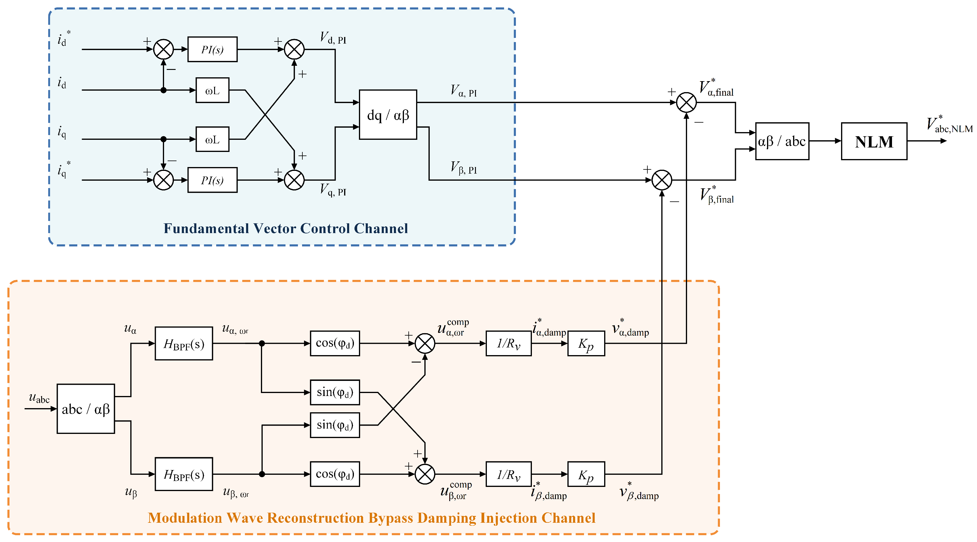
To avoid routing the damping command through the low-bandwidth integral path, this paper proposes a modulation wave reconstruction bypass injection architecture (referred to hereafter as the bypass injection method), with the control block diagram shown in
Figure 2. This control strategy retains the PI controller to focus on tracking the fundamental current in the
dq frame (the DC quantity it excels at), while the high-frequency damping command bypasses the PI controller and is directly injected at the modulation wave level in the
αβ stationary reference frame. This architecture separates the fundamental vector control channel and the high-frequency damping control channel in the frequency domain, reducing mutual interference. It should be emphasized, however, that the bypass channel is not a closed current loop at the resonance frequency. Therefore, it does not guarantee exact tracking of the commanded damping current. In practice, PCC voltage feedback, nominal delay compensation, conservative virtual resistance selection, and converter current/modulation limiting are used to keep the injected current within a positive damping operating region, but dead time, DC voltage ripple, and residual nonlinearities may reduce or distort the realized damping conductance. The proposed method should therefore be interpreted as an approximate positive damping implementation rather than an ideal regulated virtual resistance.
5.3. Implementation Steps of Bypass Injection Method
5.3.1. Extraction of Target-Frequency Harmonic Voltage
Measure the three-phase voltages
at the PCC, apply Clarke transformation to obtain
, and then extract the target harmonic component using a second-order band-pass filter (BPF) centered at
:
where
is the filter bandwidth, typically chosen as
to balance selectivity and response speed. A narrower bandwidth improves separation between adjacent harmonics but slows the response and makes the channel more sensitive to modal frequency drift; a wider bandwidth improves robustness to frequency drift but may introduce unwanted inter-harmonic components and noise. It can be verified that
, i.e., the gain is 1 and the phase shift is 0 at the center frequency, enabling distortion-free extraction.
5.3.2. Phase Compensation for Digital Delay
The MMC digital control system has a total delay of approximately
, which produces a phase lag
at the target frequency
. This value represents the nominal delay caused by sampling, calculation, and modulation update; in practice, the effective delay may vary slightly with digital implementation and modulation constraints. To ensure that the injected harmonic current is in phase with the PCC harmonic voltage as closely as possible (purely resistive response), a lead compensation is applied to the BPF output:
5.3.3. Generation of Damping Current Command
According to the virtual parallel resistance equivalent principle, when harmonic voltage
appears at the PCC, the MMC reference is designed to absorb (with the current flowing into the converter taken as positive) a damping current
5.3.4. Current-to-Voltage Command Conversion
Since the damping control is injected at the modulation voltage level after the PI output, the current command needs to be converted into an equivalent voltage command. In the vicinity of
, the effective gain of the PI controller can be approximated by the proportional gain
(the integral term contribution is negligible); therefore,
is used for the conversion:
5.3.5. Modulation Wave Reconstruction (Bypass Injection)
The MMC outer loop and PI inner loop output the fundamental voltage commands
and
in the
dq frame, which are transformed to the
αβ frame via inverse Park transformation to obtain
and
. Before NLM modulation, the fundamental modulation voltage and the damping voltage command are directly superimposed in the
αβ frame:
The physical meaning of the minus sign is: when the PCC harmonic voltage perturbs positively, the MMC output modulation voltage is reduced, inducing harmonic current to flow from the AC grid into the MMC. If implementation delays and nonlinearities are sufficiently compensated or bounded, the resulting current component is approximately in phase with the PCC harmonic voltage, so the MMC behaves as a positive conductance that absorbs harmonic energy at the resonance node. Because this high-frequency current is not directly regulated by a closed current loop, the realized conductance must be checked by EMT simulation and constrained by current and modulation limits.
The core advantage of the bypass injection method is that the high-frequency damping channel bypasses the PI controller; the PI controller focuses on zero-steady-state-error tracking of the dq-axis fundamental current, and the two channels are separated in the frequency domain. This reduces the amplitude attenuation and phase distortion caused by high-frequency signals passing through the integral path, but it also means that damping frequency current regulation is open-loop. To avoid excessive or incorrectly phased harmonic injection, the practical implementation should include a damping current limiter, a modulation index limiter, online monitoring of the extracted harmonic current phase, and blocking logic under severe unbalanced faults or converter saturation. A fully closed-loop correction of damping frequency current deviations caused by dead time, DC voltage ripple, and converter nonlinearities is beyond the scope of this paper and is identified as future work.
5.4. Multi-Mode Resonance Simultaneous Suppression Scheme
When multiple high-risk resonance modes exist simultaneously in the system (target frequencies
), independent BPFs can be designed for each target frequency (center frequency
, bandwidth
independently tuned), generating respective damping voltage commands
. These commands are linearly superimposed in the
αβ frame and then injected simultaneously:
Each BPF has a gain of 1 at its own center frequency and a gain of approximately zero at other target frequencies; therefore, the frequency-domain coupling between different damping channels is minimal when the target frequencies are well separated and the BPF bandwidths do not overlap. Equation (
17) realizes simultaneous suppression of multiple high-risk resonance modes. In the present verification, the damping channels are configured for the high-risk modes associated with the 11th and 13th LCC characteristic harmonics.
5.5. Adaptive Tuning of Virtual Conductance in Practical Applications
For practical systems with operating condition changes, the fixed offline value of
can be used as the initial value and then updated online within the admissible interval in Equation (
10). The dominant resonance frequency can be identified from PCC harmonic voltage/current measurements by a sliding-window FFT, or by an adaptive notch filter whose center frequency tracks the peak harmonic component. The modal damping trend can be estimated from the decay rate of the extracted oscillatory component after a disturbance or from the local slope of the frequency response around the identified resonance peak.
After the dominant mode is identified, the virtual conductance can be updated by either a lookup table or a recursive rule. In the lookup table method, offline modal scans similar to
Table 1 are prepared for representative grid strength and power flow conditions; the controller selects the smallest conductance that satisfies the target damping ratio and then applies interpolation between operating points. In the recursive method,
is increased step by step when the estimated damping ratio is below the target value and decreased when the damping margin is sufficient and the converter harmonic current margin becomes tight. The update should be slower than the BPF settling process, so that the damping channel does not chase measurement noise or transient estimation errors.
The adaptive loop is constrained by protection limits. The commanded damping current is saturated according to , the modulation voltage command is limited by the available modulation index, and the channel is blocked when the identified resonance frequency moves outside the BPF tuning range, when severe unbalanced faults occur, or when converter saturation is detected. Under these limits, adaptive tuning changes only the positive conductance magnitude in the selected frequency band, while the bypass-injection phase compensation maintains an approximately resistive response. This provides a practical way to retune the damping strength for different resonance modes without altering the fundamental MMC power control loop, but it is not a substitute for closed-loop correction of damping frequency current deviations.
6. Simulation Verification
6.1. Simulation System Parameter Settings
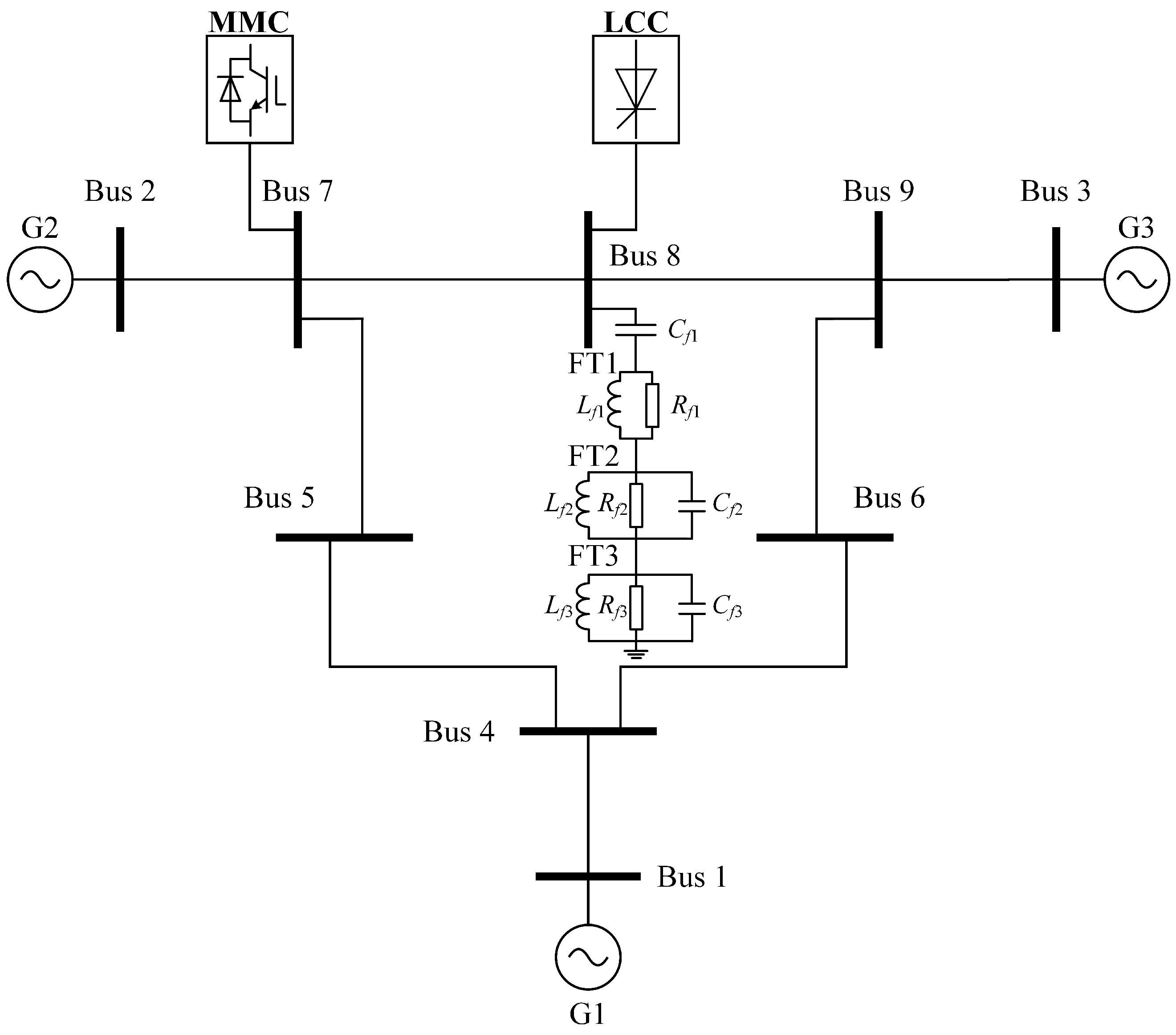
On the PSCAD/EMTDC platform, the hybrid multi-infeed receiving-end IEEE 9-bus test system shown in
Figure 1 is built. The main parameters of the system are listed in
Table 2,
Table 3,
Table 4 and
Table 5. The AC transmission branches use PSCAD coupled
π sections, with a fundamental frequency of 50 Hz and a rated line-to-line voltage of 500 kV. The inverter-side converter of LCC-HVDC is connected to bus 8, adopting a 12-pulse configuration with a DC rated voltage of 800 kV and a rated active power of 2000 MW. The inverter-side MMC-HVDC is connected to bus 7, with an AC rated voltage of 525 kV, a DC rated voltage of 800 kV, a rated power of 2000 MW, and a control period
= 50 μs. The MMC equivalent resistance is 1.5 Ω, the transformer equivalent inductance is 0.04785 H, the arm inductance is 0.1608 H, and the total equivalent inductance is 0.1864 H.
6.2. Resonance Modal Analysis and High-Risk Mode Identification
Using the two-stage
s-domain nodal admittance matrix method, a wideband resonance mode scan is performed on the system of
Figure 1, and the calculation results are shown in
Table 6. The system exhibits three main resonance modes in this frequency band, denoted as #1, #2, and #3.
Mode #1 has a resonance frequency of 147.76 Hz, which is close to the first tuning point (150 Hz) of the triple-tuned filters (FT1–FT3). Its maximum shape node is the filter internal node FT1, while the shape magnitudes of the main network nodes (Bus1–Bus9) are all below 0.022, indicating a local resonance confined within the filter branch and not posing a system-wide risk.
Mode #2 has a resonance frequency of 581.31 Hz, lying between the LCC’s 11th (550 Hz) and 13th (650 Hz) characteristic harmonics, with an extremely low damping ratio of 0.64%. The mode shape eigenvector shows that the LCC connection point (Bus8) and the MMC connection point (Bus7) have magnitudes as high as 1.0000 and 0.9875, respectively, both being core areas of voltage amplification. This indicates that once the LCC injects the 11th or 13th harmonic current, strong harmonic voltage amplification will be excited at Bus7 and Bus8 and propagated throughout the network. Therefore, Mode #2 is identified as the primary high-risk resonance mode, and Bus8 or Bus7 is the optimal location for implementing active damping.
Mode #3 has a resonance frequency of 798.85 Hz with a damping ratio as low as 0.52%, but its frequency deviates significantly from the LCC characteristic harmonics (e.g., 23rd at 1150 Hz). Moreover, the maximum shape node is Bus4, while the shape magnitudes at the DC feed-in nodes Bus7 and Bus8 are relatively small (0.45–0.56). The risk of being directly excited by LCC characteristic harmonics is relatively low, and this mode does not require immediate suppression but warrants monitoring.
The harmonic voltage and current amplitudes at buses 1 to 9 obtained from PSCAD simulation are shown in
Table 7 and
Table 8, respectively. The simulation data further corroborates the above analysis: the 11th harmonic voltages at Bus7 and Bus8 reach 27.31 kV and 33.20 kV, respectively, and the 13th harmonic voltages reach 11.98 kV and 10.13 kV, far exceeding the levels in non-resonant frequency bands. This verifies that the extremely weak damping of Mode #2 causes significant amplification of LCC characteristic harmonics. Therefore, Bus8 and Bus7 are taken as priority implementation nodes for active damping control, with the suppression strategy focused on Mode #2.
6.3. Active Damping Control Effectiveness Verification
Based on the
s-domain nodal admittance matrix analysis and the virtual resistance sensitivity results in
Table 1, the MMC connection node Bus7 is configured with virtual damping control, making it equivalent to a parallel resistance
= 35 Ω at the 11th harmonic frequency. This raises the damping ratio of Mode #2 from 0.64% to 38.49%. Considering that the resonance mode may shift after the virtual impedance control is applied, the same control parameters are also deployed at the 13th harmonic frequency to cover the main injection bands of LCC characteristic harmonics. After applying active damping, the system resonance modes obtained from
s-domain analysis are shown in
Table 9.
It can be seen that the originally high-risk Mode #2 is effectively suppressed: its resonance frequency shifts from 581.31 Hz to 643.22 Hz, and the damping ratio increases from 0.64% to 38.49% (approximately 60 times), far exceeding the engineering requirement of . Notably, the damping ratio of Mode #3 is also raised from 0.52% to 6.39%, even though this mode was not directly targeted. This improvement arises because Bus7 has a non-negligible mode shape magnitude of 0.4461 in Mode #3; the virtual conductance shunted at Bus7 increases the overall system dissipation and benefits all modes in which Bus7 participates.
It is worth noting that the mode shape eigenvectors in
Table 9 remain identical to those in
Table 6. This is because the virtual parallel resistance acts as a shunt admittance to ground at Bus7, which modifies only the self-admittance (diagonal) element of
at that node. According to the two-stage method, the mode shape eigenvectors are extracted from the susceptance matrix
in Stage 1, which is unaffected by purely resistive shunts. Physically, the damping control does not alter the network’s reactive power flow paths, and the relative voltage distribution pattern is therefore preserved. To further verify the performance, time-domain simulations are conducted in PSCAD/EMTDC. The simulation sequence is as follows: at
t = 2 s, characteristic harmonic currents containing the 11th and 13th orders are injected at the LCC connection node Bus8; at
t = 4 s, the proposed active damping control is activated.
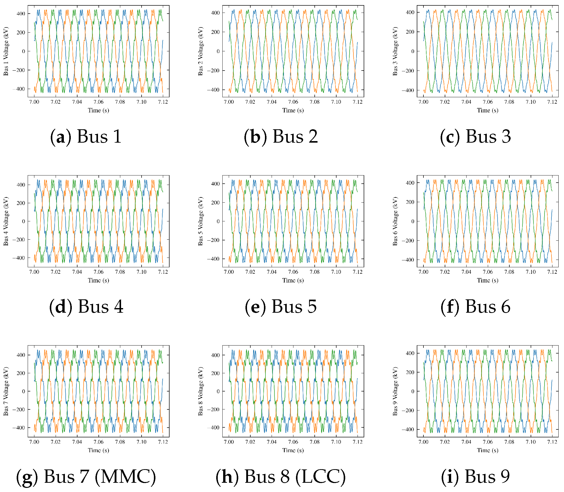
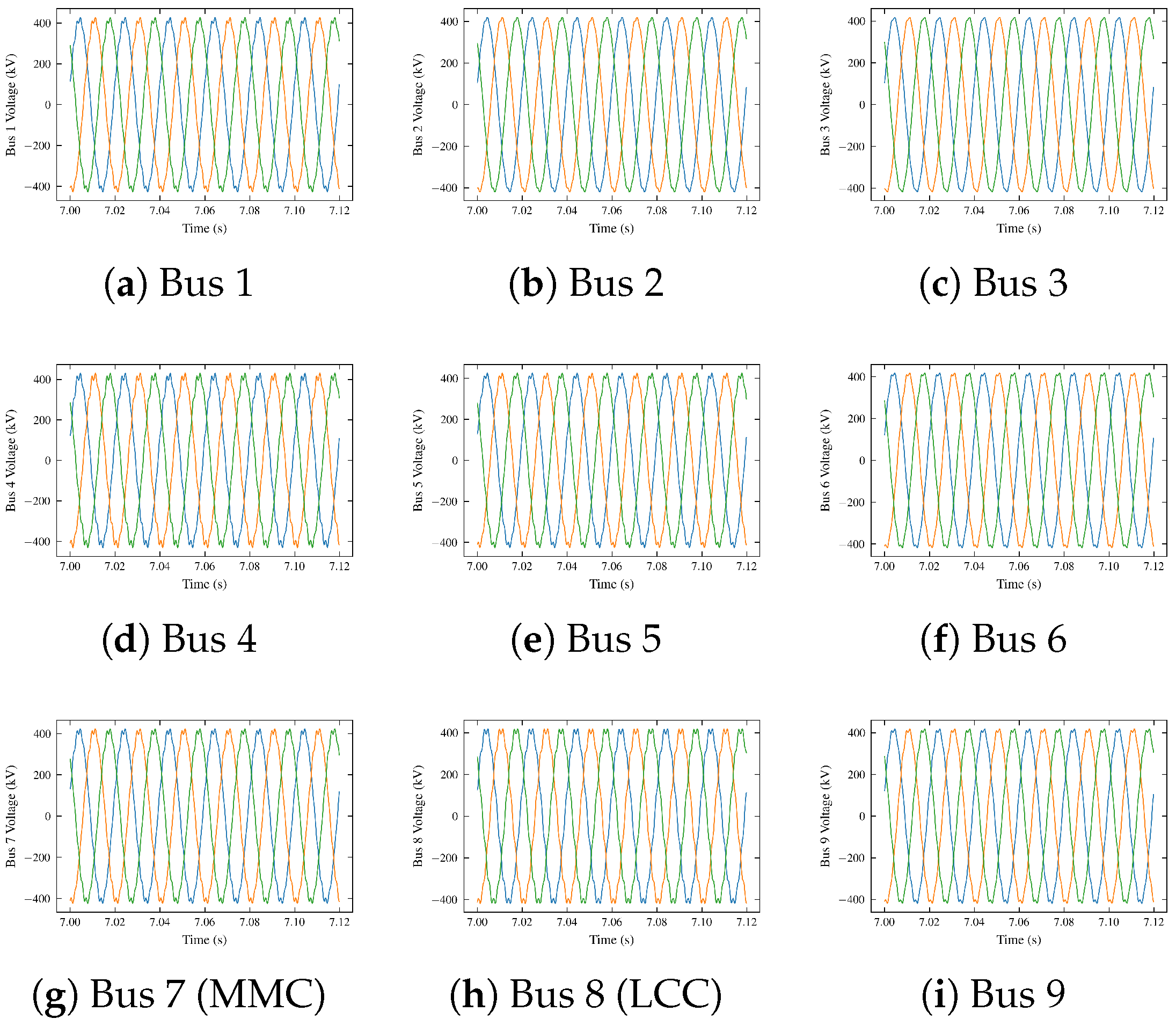
Figure 3 shows the three-phase voltage waveforms at buses 1–9 without active damping control, and
Figure 4 shows the corresponding waveforms with active damping control. In these figures, the horizontal axis is time in seconds and the vertical axis is phase voltage in kV.
After the active damping control is enabled, the harmonic voltage and current amplitudes at buses 1 to 9 are shown in
Table 10 and
Table 11. From the simulation results:
t = 2∼4 s (before control): the 11th harmonic voltages at Bus8 and Bus7 reach 33.20 kV and 27.31 kV, respectively, while the 13th harmonic voltages reach 10.13 kV and 11.98 kV, indicating severe harmonic amplification;
t > 4 s (after control): the 11th harmonic voltage at Bus8 drops to 10.27 kV (69.1% reduction) and at Bus7 to 3.34 kV (87.8% reduction); the 13th harmonic voltage at Bus8 decreases to 1.68 kV (83.4% reduction) and at Bus7 to 5.57 kV (53.5% reduction).
Comparing the fundamental current data before and after control shows that the fundamental currents in each branch change very little (deviation less than 0.1%), and the active power at the PCC remains stable. This confirms that the proposed bypass injection architecture effectively separates the high-frequency damping channel from the fundamental vector control channel: the PI controller concentrates on zero-steady-state-error tracking of the fundamental, while the high-frequency damping command bypasses the PI controller and is superimposed directly on the modulation wave. The two channels work cooperatively with little mutual interference, suppressing the target resonance without affecting the normal power transmission of the MMC.
In summary, the simulation results verify the following: (1) the virtual resistance value
= 35 Ω, selected from the modal-sensitivity trade-off in
Table 1, substantially improves the damping of the high-risk resonance mode while maintaining a bounded damping current demand; (2) the bypass injection architecture realizes an approximate virtual resistance characteristic, so that the MMC behaves as a positive damping conductance for harmonic energy absorption at the target frequency without disturbing fundamental power transmission; and (3) the simultaneous suppression scheme for the 11th and 13th harmonics is effective in the studied case, with independently tuned channels and minimal cross-coupling.