

Article

Investigation on Degradation of Switching Characteristics in SiC MOSFETs Under Repetitive Surge Current

1
Institute of Novel Semiconductors, Shandong University, Jinan 250100, China
2
Beijing Huairou Laboratory, Beijing 101409, China
*
Author to whom correspondence should be addressed.
Electronics 2026, 15(12), 2721; https://doi.org/10.3390/electronics15122721
Submission received: 2 May 2026 / Revised: 28 May 2026 / Accepted: 9 June 2026 / Published: 19 June 2026
(This article belongs to the Section Power Electronics)

Abstract

Surge reliability is a crucial aspect of silicon carbide (SiC) metal-oxide-semiconductor field-effect transistor (MOSFET) reliability. This study investigates the degradation behavior and mechanisms of switching characteristics in 1.2 kV planar-gate SiC MOSFETs under repetitive surge current. A surge current test platform is established to conduct surge tests on the device, while monitoring the evolution of its switching characteristics. The results indicate that after 4000 surge current cycles, the device’s turn-on delay time (td(on)), rise time (tr), and turn-on loss (EON) show no significant changes. In contrast, the turn-off delay time (td(off)), fall time (tf), and turn-off loss (EOFF) increase by 9%, 7.5%, and 8.3%, respectively. Switching characteristics variations are closely linked to the reduction in threshold voltage (VTH) and the increase in gate-source capacitance (CGS) and gate-drain capacitance (CGD). The degradation of these parameters stems from the accumulation of positive trapped charge in the gate oxide layer above the channel and junction field-effect transistor (JFET) region. The increase in charges results from the combined effects of negative gate bias and cyclic high temperature induced by repetitive surge current. This study provides a theoretical basis for the comprehensive understanding of the impact of surge current on SiC MOSFET performance.

1. Introduction

Compared with traditional silicon-based devices, silicon carbide (SiC) metal-oxide-semiconductor field-effect transistors (MOSFETs) have been widely adopted in fields such as electric vehicles, renewable energy, and industrial drives [1,2], owing to their advantages of high switching speed, low loss, and high-temperature tolerance [3,4]. For long-term applications, the reliability evaluation of SiC MOSFETs is particularly critical. Among various tests, power cycling testing is one of the most important reliability experiments for assessing a device’s long-term operational capability [5,6]. This test primarily simulates actual normal operating conditions and can effectively evaluate the device’s lifetime. However, the device’s performance under extreme conditions, such as surge current, is equally important. Surge current refers to an instantaneous overload current significantly exceeding the steady-state operating current of the circuit, typically triggered by converter faults [7,8,9] or transient charging of capacitive loads during system startup [10,11]. In power converter design, to achieve higher power density and lower costs, the high-performance parasitic body diode of SiC MOSFETs is often leveraged to directly replace the external anti-parallel diode [12,13]. This results in the body diode becoming the primary conduction path for surge current. During service, SiC MOSFETs may endure repetitive surge current impacts, subjecting the devices to cyclic high-temperature and high-current stress. Such conditions can induce performance degradation in the devices, thereby affecting overall system efficiency. Consequently, conducting repetitive surge tests on SiC MOSFETs and investigating the degradation behavior and physical mechanisms hold significant academic value and engineering significance.
Existing studies have investigated this issue. Ma et al. [14] conducted repetitive surge tests on SiC MOSFETs under negative gate bias, observing negative drift in threshold voltage (VTH), increased gate leakage current (IGSS), elevated on-resistance (RDS(ON)), and increased body diode forward voltage drop (VSD). The degradation primarily originates from bond wire aging and gate oxide damage. Zhu et al. [15] performed tests under gate-source short-circuit condition and noted no significant VTH drift, but observed increases in VSD and RDS(ON), with bipolar degradation being the dominant mechanism. Jiang et al. [16] investigated the effects of surge current magnitude, gate turn-off voltage, and stress cycles on devices, finding significant drift in static parameters such as VTH, RDS(ON), VSD, and drain leakage current (IDSS). Wang et al. [17] conducted repetitive surge tests on asymmetric trench SiC MOSFETs under different gate voltages and ambient temperatures, similarly observing negative VTH shift and increases in VSD and RDS(ON). Zhan et al. [18] evaluated surge reliability in a series of planar-gate SiC MOSFETs with different P-well designs under gate-source voltage (VGS) of −10 V, noting varying degrees of degradation in static characteristics. These studies uncover the performance degradation and underlying mechanisms in SiC MOSFETs under repetitive surge current, yet all focus on static characteristics and pay insufficient attention to the degradation of dynamic characteristics (switching characteristics). As switching devices, the dynamic characteristics of SiC MOSFETs are equally critical.
To address this gap, this paper conducts repetitive surge tests on SiC MOSFETs, focusing on the degradation behavior and mechanisms of their switching characteristics. After subjecting the devices to repetitive surge current stress, the turn-on process exhibits minimal changes, while the turn-off process is significantly affected. These alterations are considered closely related to the degradation of VTH, gate-source capacitance (CGS), and gate-drain capacitance (CGD). The observed parametric shifts are attributed to an increase in positive trapped charge density within the oxide layer overlying the channel and junction field-effect transistor (JFET) regions.

2. Materials and Methods

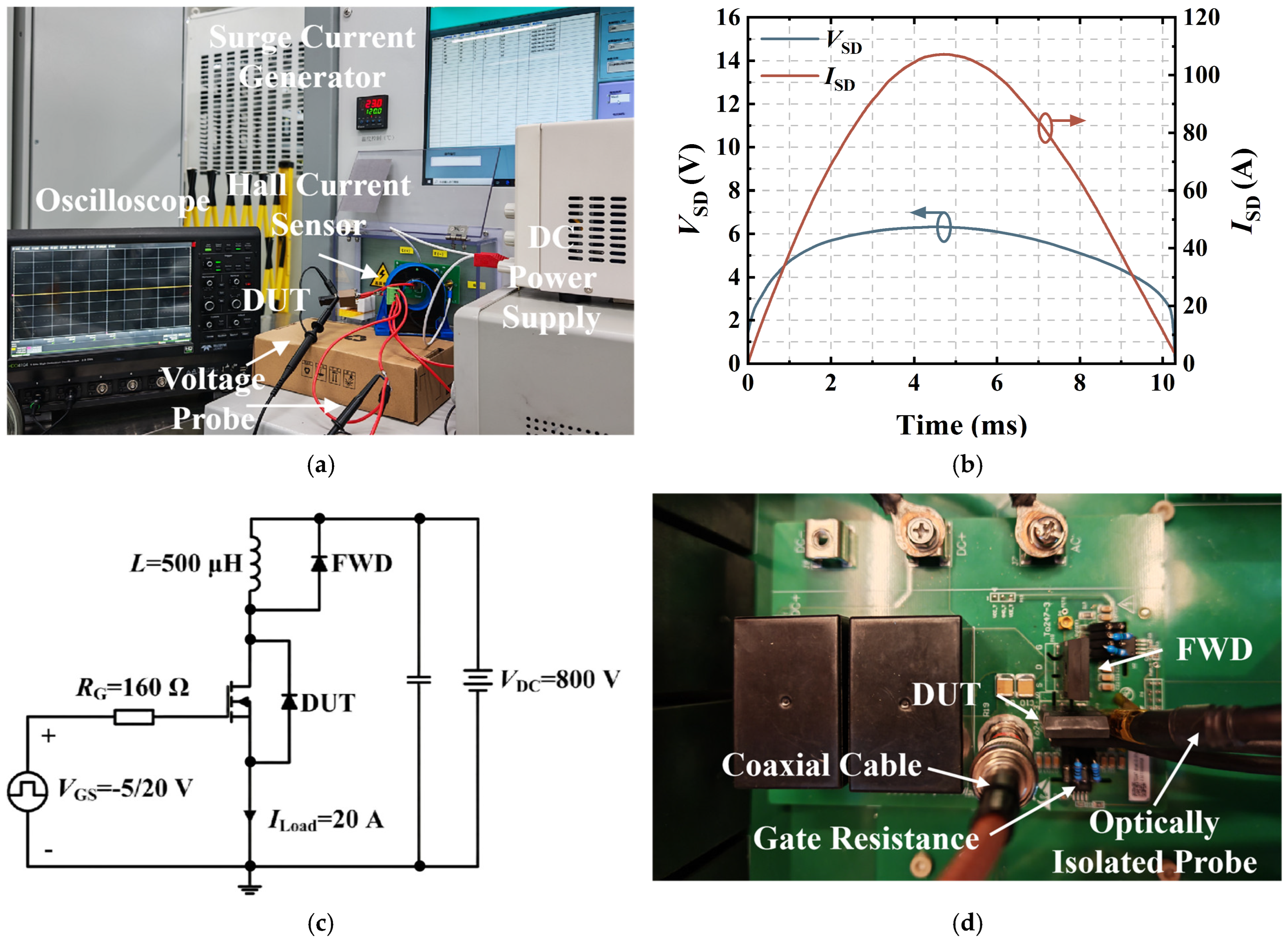
A surge current generator is used to produce a half-sinusoidal surge current with a peak of 110 A, corresponding to about three times the rated current (36 A) and 60% of the maximum surge withstand capability (about 190 A). This level is selected to induce observable cumulative degradation while avoiding premature failure. The pulse duration is set to 10 ms to simulate the surge waveform typical of a 50 Hz AC grid fault. A 20 s interval between consecutive surge pulses is implemented to allow sufficient heat dissipation, ensuring that the device fully cools down before each surge stress application. This guarantees that every stress cycle starts from an identical thermodynamic initial state. Consequently, the observed performance degradation can be attributed solely to the cumulative damage from repeated electrical-thermal stress, thereby eliminating any interference from thermal accumulation in the analysis of the degradation mechanism. During testing, the device under test (DUT) is biased at a gate-source voltage of −5 V by a DC power supply. This setup ensured that during surge events, the current is confined to the body diode. The corresponding source-drain current (ISD) and voltage (VSD) waveforms are measured using a Hall-effect current sensor and a passive voltage probe, respectively, as shown in Figure 1b.
The electrical characterization of the DUT is conducted at every 1000-cycle interval, during which the surge current test is temporarily paused. This procedure is repeated until a gate-source short-circuit failure occurs after 4200 cycles. To characterize switching characteristics, the double-pulse test circuit shown in Figure 1c is utilized. The upper arm employs a device identical to the DUT, with its VGS set to −5 V to ensure current flow through its body diode during freewheeling. For the DUT, the turn-off gate voltage (VGoff) is set to −5 V, the turn-on gate voltage (VGon) to 20 V, and the DC bus voltage (VDC) to 800 V. The load inductance (L) is 500 μH, and the load current (ILoad) is set to 20 A. To amplify the degradation of switching characteristics, the external gate resistance (RG) is set to 160 Ω. Figure 1d shows the printed circuit board (PCB) used for the double-pulse test. During testing, the DUT’s drain-source voltage (VDS) is measured using a differential voltage probe, the drain-source current (IDS) via a coaxial cable, and VGS using an optically isolated probe. To analyze the causes of switching characteristics degradation, the transfer characteristics and parasitic capacitances of the DUT are measured before and after repetitive surge current using an Agilent B1500A Semiconductor Analyzer (Keysight Technologies, Santa Rosa, CA, USA). For transfer characteristics, the gate and drain are shorted (VG = VD), and VTH is extracted at IDS = 10 mA. For parasitic capacitance characterization, the gate and source are shorted (VG = VS) with a small-signal frequency f = 1 MHz and AC amplitude VAC = 25 mV. Additionally, to assess the degradation of the oxide layer, the capacitance-voltage (C-V) characteristics are measured using an Agilent E4990A Impedance Analyzer (Keysight Technologies, Santa Rosa, CA, USA) before and after repetitive surge current, with the drain and source shorted (VD = VS), f = 1 MHz, and VAC = 25 mV. The high measurement frequency of 1 MHz minimizes the contribution of interface states to the capacitance, thereby facilitating the analysis of the polarity and distribution of oxide trap charges [19]. All tests are conducted at room temperature (25 °C). To ensure the reproducibility and reliability of the results, three DUTs are employed in the experiments.

3. Results

3.1. Degradation of Switching Characteristics

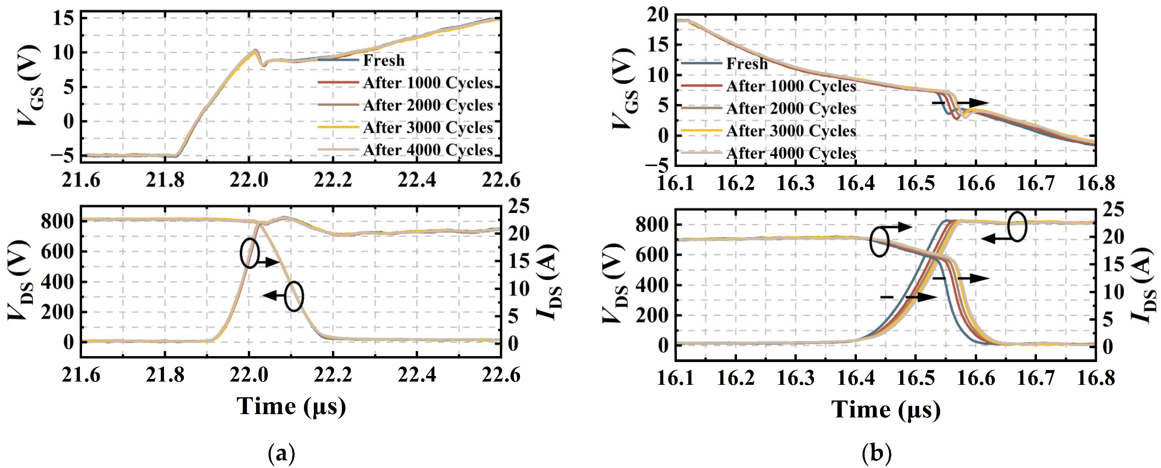
Figure 2a and Figure 2b, respectively, illustrate the evolution of the device’s turn-on and turn-off waveforms with increasing surge current cycles. It can be observed that the turn-on waveforms remain essentially unchanged, while the turn-off waveforms exhibit a significant delay.
To quantitatively characterize the degradation of the switching characteristics, the switching times and switching losses are extracted. The switching times include the turn-on time (ton) and turn-off time (toff), where ton comprises the turn-on delay time (td(on)) and rise time (tr), while toff comprises the turn-off delay time (td(off)) and fall time (tf). Switching losses include the turn-on loss (EON) and turn-off loss (EOFF). The sum of the two is the total loss (ESW). The extraction of all these parameters strictly adheres to the IEC 60747-8 standard [20].
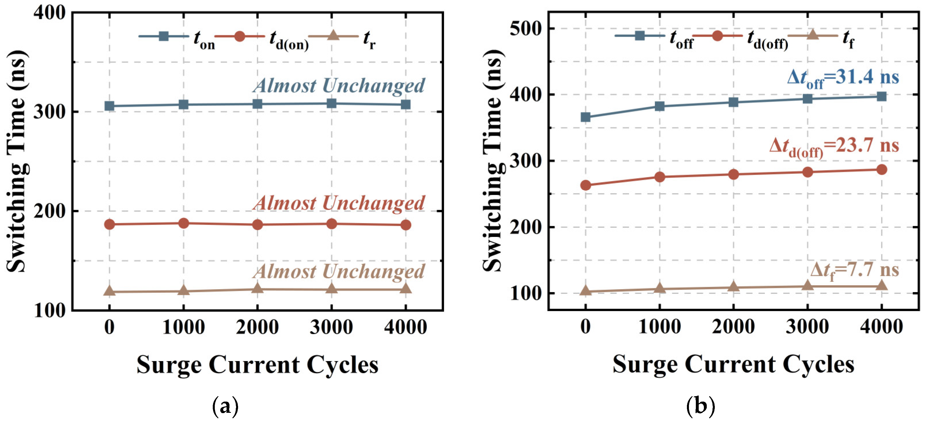
Figure 3a,b presents the variations of switching times with increasing surge current cycles, respectively. It can be observed that as the cycle count increases, td(on) and tr remain essentially unchanged, resulting in nearly constant ton. In contrast, td(off) and tf progressively increase, leading to prolonged toff. After 4000 surge current cycles, the DUT exhibits a 23.7 ns extension in td(off) (a 9% increase) and a 7.7 ns extension in tf (a 7.5% increase). To investigate the primary causes of these switching time variations, the following expressions may be analyzed [21,22]:
t d ( on ) = R G ( C GS + C GD ) ln ( V Gon V Goff V Gon V GP ) ,
t r = C GD R G V Gon V GP V DC ,
t d ( off ) = R G ( C GS + C GD ) ln ( V Gon V GP ) ,
t f = C GD R G V GP V Goff V DC .
Here, VGP denotes the Miller plateau voltage. CGS, CGD, and VGP are susceptible to variations induced by gate bias and surge current, while other parameters such as RG, VGon, VGoff, and VDC remain unaffected and essentially constant. Therefore, according to Equation (1), the change in td(on) is primarily dominated by CGS, CGD, and VGP. It should be noted that during the td(on) phase, the DUT is subjected to a VDC of approximately 800 V. At this point, CGD is at its minimum value CGD,min. Consequently, (CGS + CGD) is predominantly determined by CGS, because CGD,min is negligible compared to CGS [23]. Additionally, combining with the expression [24]
V GP = V TH + J on W cell L ch 2 μ ni C ox ,
VGP is determined by VTH. Therefore, the variation in td(on) is primarily influenced by changes in CGS and VTH. Based on the above analysis and combining Equations (2) and (4), the variations in tr and tf are mainly affected by CGD and VTH. During these two phases, VDS undergoes significant changes. Since CGD is strongly modulated by VDS, its value also experiences substantial variations. Thus, more accurately, CGD here should be represented by its average value, CGD,av. Similarly, td(off) is affected by CGS, CGD, and VTH, as shown in Equation (3). However, during this phase, the VDS of the DUT is relatively small (approximately equal to the on-state voltage), and VGS > VTH. Consequently, (CGS + CGD) approximates the gate oxide capacitance COX. This capacitance is less susceptible to gate bias and surge current influences, so the variation in td(off) is primarily determined by VTH.
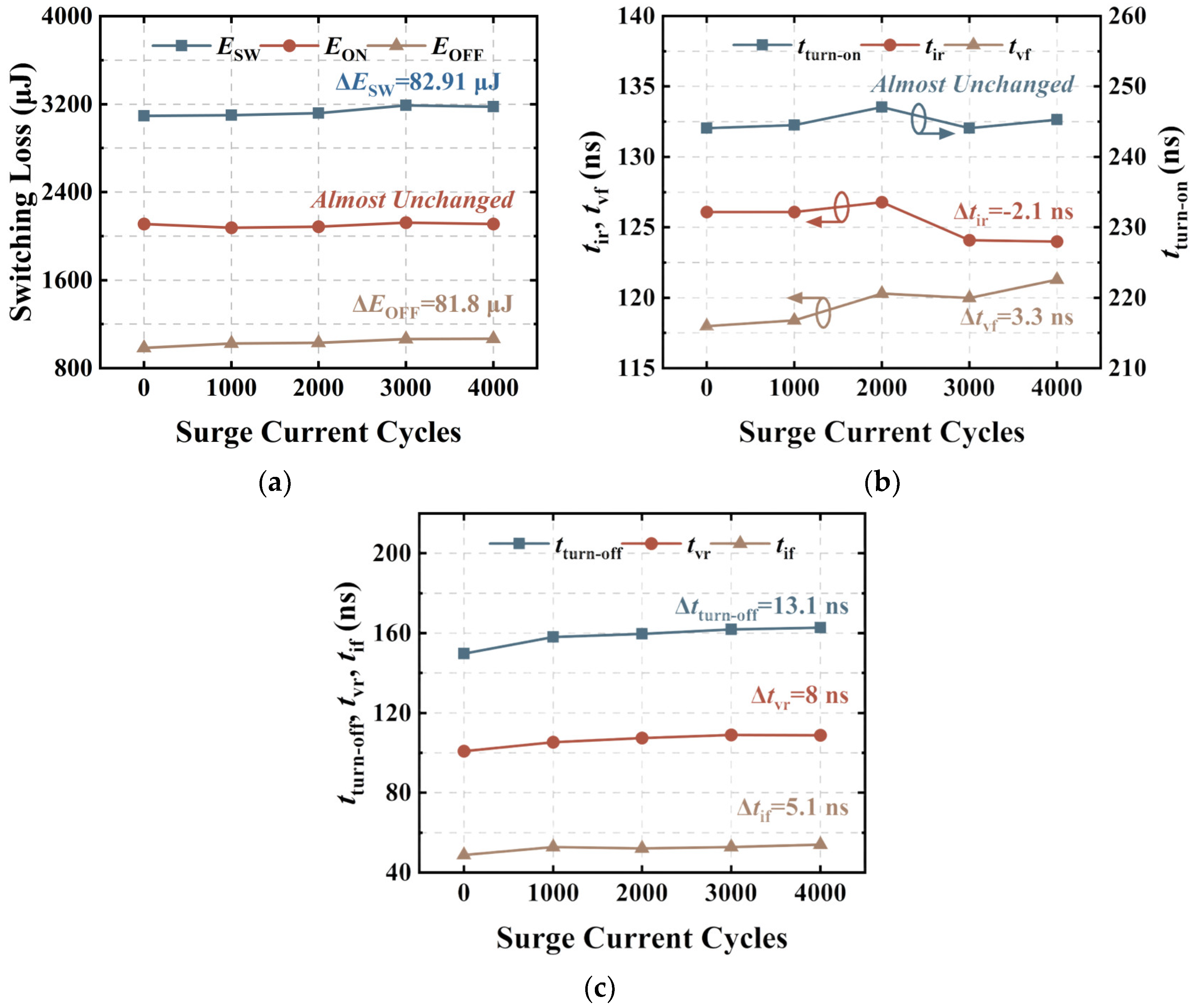
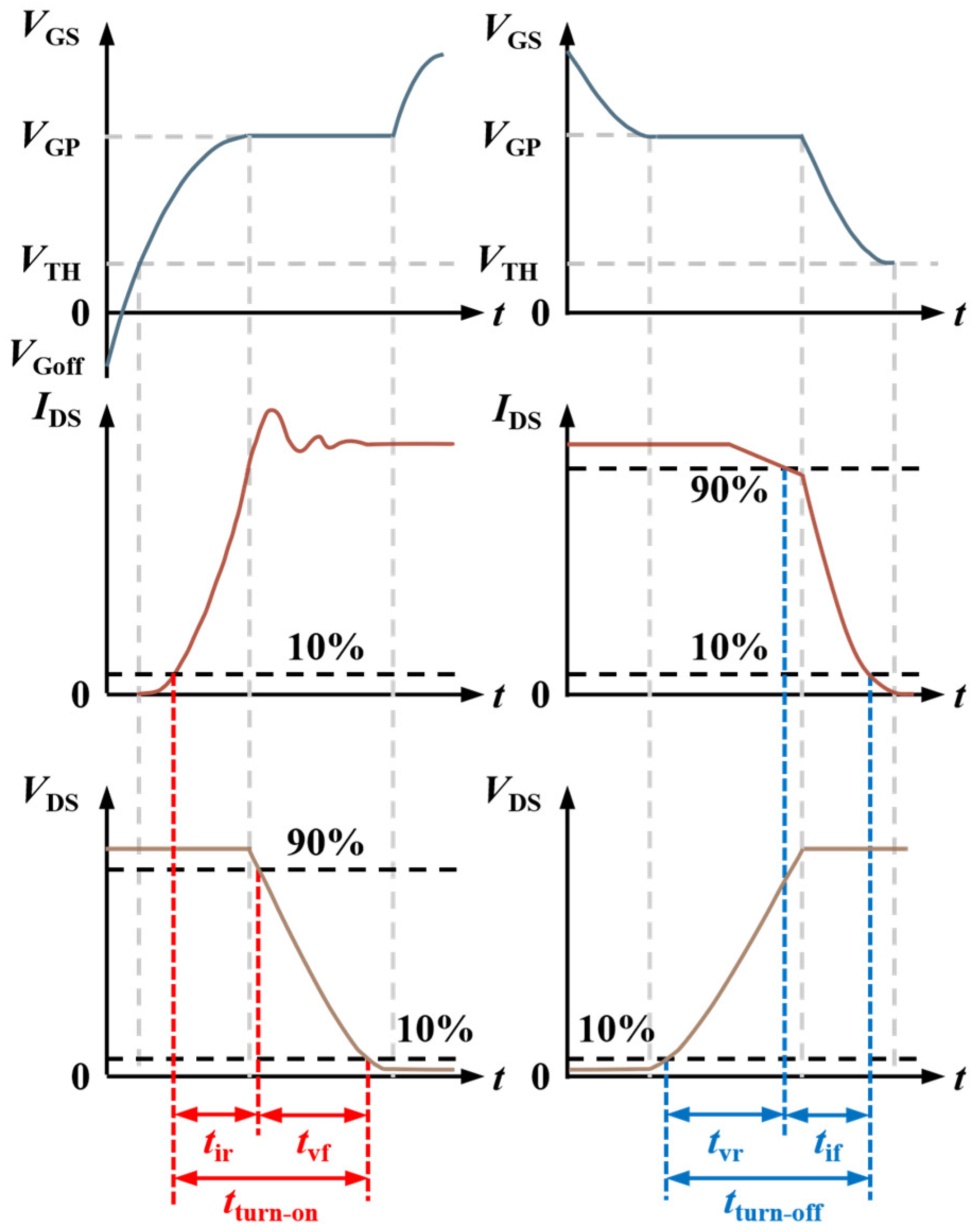
Figure 4a shows the variations of ESW, EON, and EOFF with increasing surge current cycles. It can be observed that as the number of cycles increases, EON remains essentially unchanged, while EOFF continuously rises, leading to a corresponding increase in ESW. After 4000 cycles, EOFF increases by 81.8 μJ, representing an 8.3% increase. The changes in switching losses can be explained by variations in their corresponding integration times [25]. Integration time refers to the time window over which the product of VDS and IDS is integrated to extract the switching loss, including the turn-on integration time (tturn-on) and the turn-off integration time (tturn-off). Furthermore, tturn-on can be expressed as the sum of the current rise time (tir) and the voltage fall time (tvf), while tturn-off can be expressed as the sum of the voltage rise time (tvr) and the current fall time (tif). The definitions of these time intervals are shown in Figure 5 [25]. Switching loss, which stems from the overlap of IDS and VDS, is directly proportional to the integration time: a longer time increases the loss, while a shorter time reduces it. Figure 4b,c, respectively, shows the trends of tturn-on and tturn-off with increasing surge current cycles. It can be seen that tturn-on shows almost no change; hence, EON remains essentially stable. Conversely, tturn-off gradually lengthens with increasing cycles, causing EOFF to increase accordingly. It can also be observed that the stability of tturn-on stems from the offsetting effects of a shortened tir and a lengthened tvf: after 4000 cycles, tir shortens by 2.1 ns (a decrease of approximately 1.7%), while tvf lengthens by 3.3 ns (an increase of approximately 2.8%). On the other hand, the increase in tturn-off is caused by the simultaneous lengthening of both tvr and tif. After the same 4000 cycles, tvr lengthens by 8 ns (an increase of about 8%), and tif lengthens by 5.1 ns (an increase of about 10.4%). The main reasons for the changes in integration time can be analyzed through the following equations [26]:
t ir = R G ( C GS + C GD ) ln ( V Gon V TH V Gon V GP ) ,
t vf = R G Q GD V Gon V GP ,
t vr = R G Q GD V GP V Goff ,
t if = R G ( C GS + C GD ) ln ( V GP V TH V Goff ) .
Among them, QGD represents the gate-drain charge. According to Equation (6), the variation in tir is primarily influenced by CGS, CGD, and VTH. However, during this stage, the DUT satisfies VGS > VTH, and the channel is in a strong inversion state. At this point, CGS can be regarded as the oxide layer capacitance, which is less susceptible to gate bias and surge current influences. Simultaneously, since VDSVDC, CGD is at its minimum value CGD,min, which is negligible compared to CGS. Therefore, the variation in tir is actually dominated solely by VTH. Based on Equations (7) and (8), tvf and tvr are mainly affected by QGD and VGP (i.e., VTH). The magnitude of QGD is proportional to CGD,av. Similarly, according to Equation (9), tif is also influenced by CGS, CGD, and VTH. Based on the same mechanism as tir, its variation is ultimately determined solely by VTH.
Figure 4. Variations in switching losses and integration times with increasing surge current cycles. (a) Total loss (ESW), turn-on loss (EON), and turn-off loss (EOFF); (b) turn-on integration time (tturn-on), current rise time (tir), and voltage fall time (tvf); (c) turn-off integration time (tturn-off), voltage rise time (tvr), and current fall time (tif).
Electronics 15 02721 g004
Figure 5. The schematic diagram of integration time definition.
Electronics 15 02721 g005

3.2. Degradation Mechanism Analysis

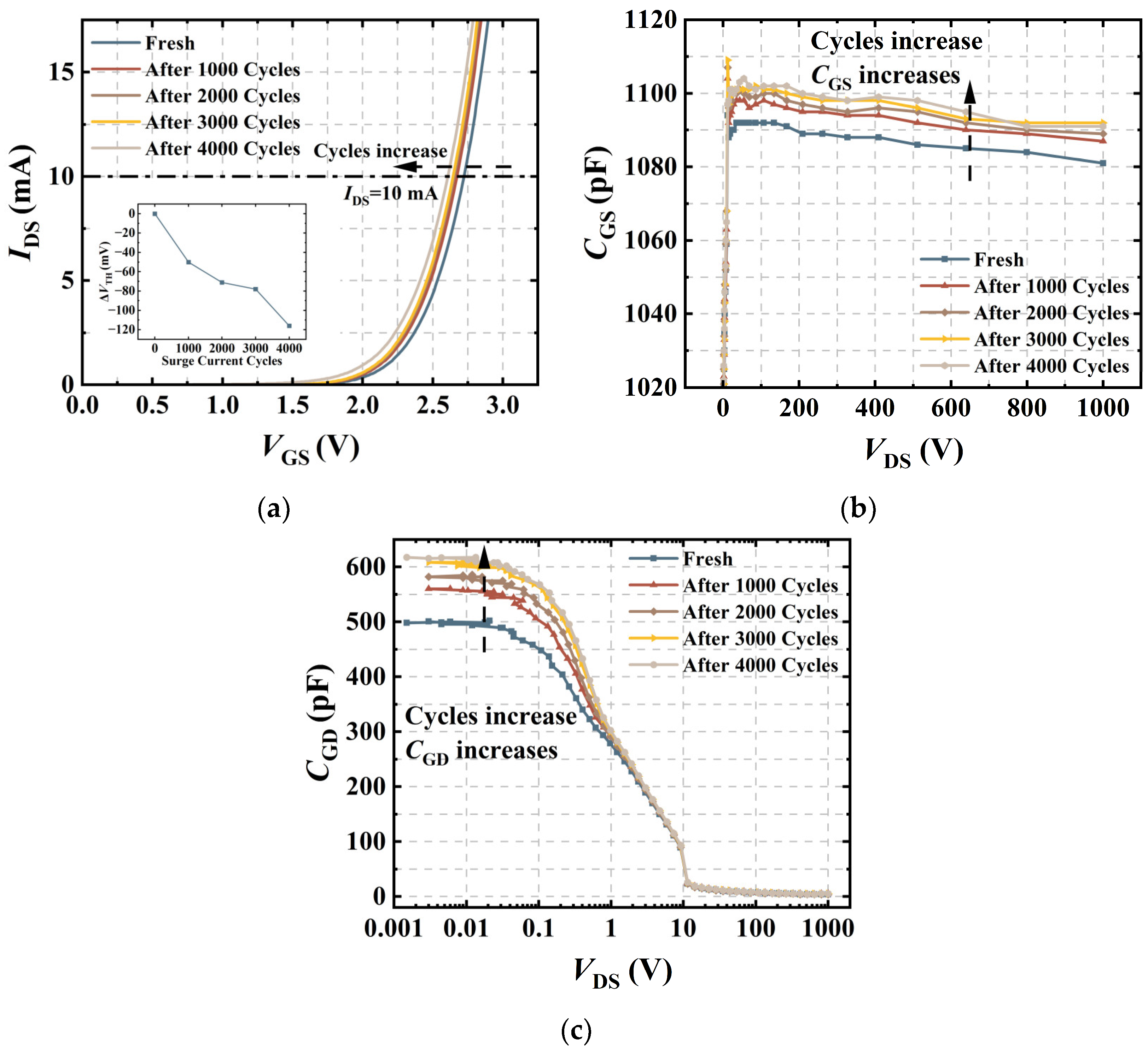
In light of the preceding analysis, VTH, CGS, and CGD emerge as the key parameters governing the device’s switching times and losses (integration times). Therefore, this paper monitors these key parameters. Figure 6a, b, and c shows the variations in the transfer characteristics curve, CGS-VDS curve, and CGD-VDS curve with increasing cycle numbers, respectively. A negative VTH shift of approximately 0.12 V is observed after 4000 surge current cycles. CGS increases across the entire VDS range with increasing cycles. In contrast, CGD increases only within the low VDS range and remains largely unchanged at high voltage. Consequently, CGD,av gradually increases with the number of cycles.
Based on the trends of the key parameters described above, the drift mechanisms of switching times and integration times can be reasonably explained. Regarding switching times, the stability of td(on) is attributed to the counteracting effects of decreased VTH and increased CGS: Equation (1) indicates that a reduction in VTH shortens td(on), while an increase in CGS lengthens it, resulting in minimal overall change. Similarly, the stability of tr arises from the combined influence of decreased VTH and increased CGD,av: according to Equation (2), lower VTH reduces tr, while higher CGD,av extends it, leading to overall stability. The lengthening of td(off) primarily stems from reduced VTH, as shown in Equation (3), while the extension of tf is jointly caused by decreased VTH and increased CGD,av, as specified in Equation (4). Regarding integration times, based on Equations (6) and (9), both the shortening of tir and lengthening of tif originate from reduced VTH. The extension of tvf is predominantly driven by increased CGD,av, as described in Equation (7). The lengthening of tvr arises from the synergistic effects of reduced VTH and increased CGD,av, as established in Equation (8).
The observed decrease in VTH results from a higher positive trapped charge density (Qpos) in the oxide. The expression for VTH is given by [27]
V TH = 4 ε S k T N B ln N B / n i C OX + 2 k T q ln N B n i + Φ ms Q pos C OX + Q neg C OX ,
where εS is the absolute permittivity of SiC, Φms represents the work function difference between the gate material (poly-Si) and SiC, COX denotes the oxide capacitance, k is Boltzmann’s constant, T is absolute temperature, NB is the doping concentration, ni is the intrinsic carrier concentration, and q is the electron charge. All of these parameters remain constant under stress conditions. Only Qpos and Qneg, representing the density of positive and negative trapped charge, respectively, are susceptible to gate bias and surge current influences. Consequently, the negative shift in VTH is attributed to an increase in Qpos. These charges create an assisting electric field that lowers VTH by promoting inversion layer formation.
The increase in CGS and CGD can be attributed to the accumulation of Qpos in the gate oxide overlying the channel and JFET regions, respectively. Under gate-source short-circuit conditions, this Qpos buildup in the channel oxide generates an electric field that reduces the P-well depletion width. Because capacitance is inversely proportional to depletion width, the narrowing directly raises CGS. Similarly, Qpos accumulation in the oxide above the JFET region attracts more electrons, narrowing the depletion layer in that area. This results in an increase in CGD at low VDS. However, at high VDS, the depletion layer expands significantly. This expansion diminishes the modulating effect of Qpos on the depletion layer, rendering CGD nearly unchanged under high VDS.
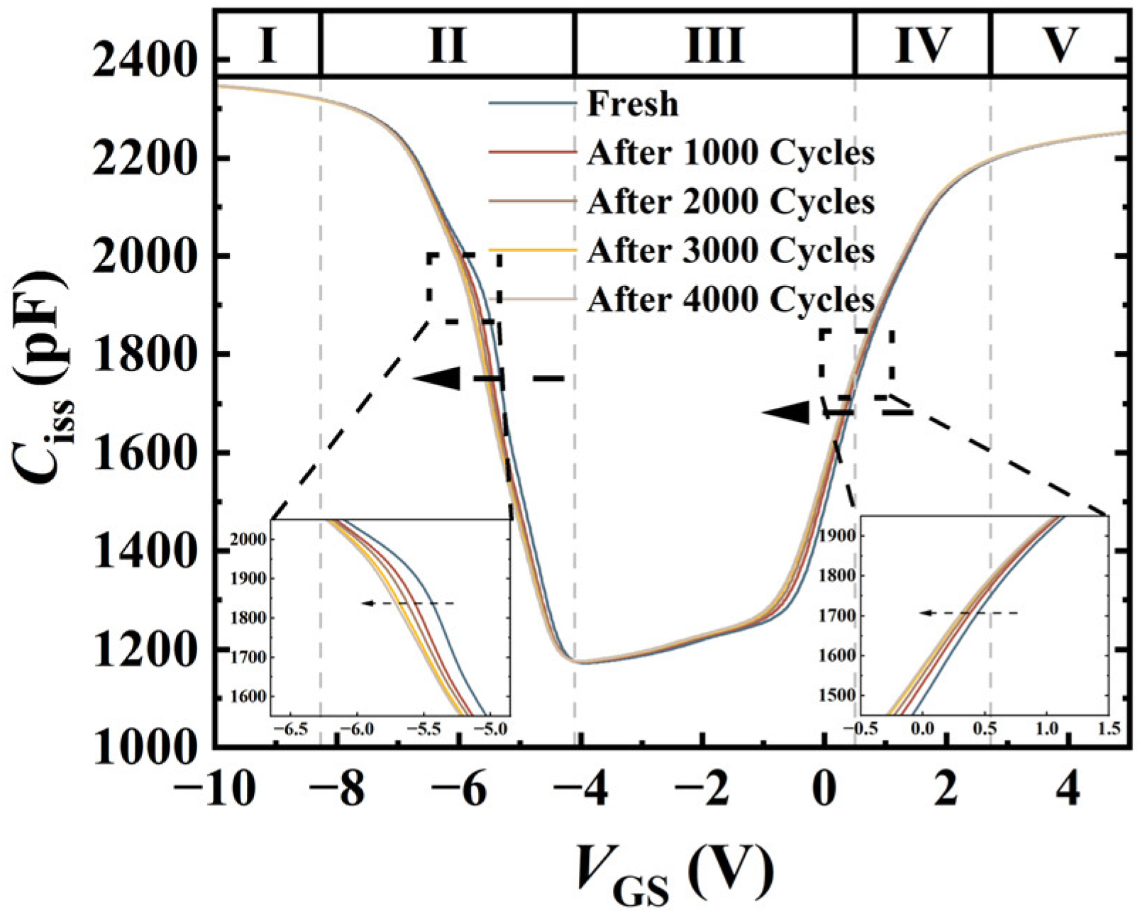
Therefore, the observed drift in VTH, CGS, and CGD is primarily due to the accumulation of Qpos in the gate oxide overlying the channel and JFET regions. To verify this conclusion, C-V characterization is performed on the device pre- and post-repetitive surge current stress, with the results presented in Figure 7. According to the interface damage theory, the C-V curve is typically divided into five regions [19]. The results reveal that as the surge cycles increase, the curves in Region II and Region IV both exhibit a negative shift. This shift is a characteristic signature of increased Qpos in the gate oxide. The shift in Region II indicates degradation of the JFET region’s gate oxide, while the shift in Region IV corresponds to degradation above the channel region. These results directly confirm that Qpos accumulation occurs in the gate oxide overlying the channel and JFET regions after repetitive surge current.
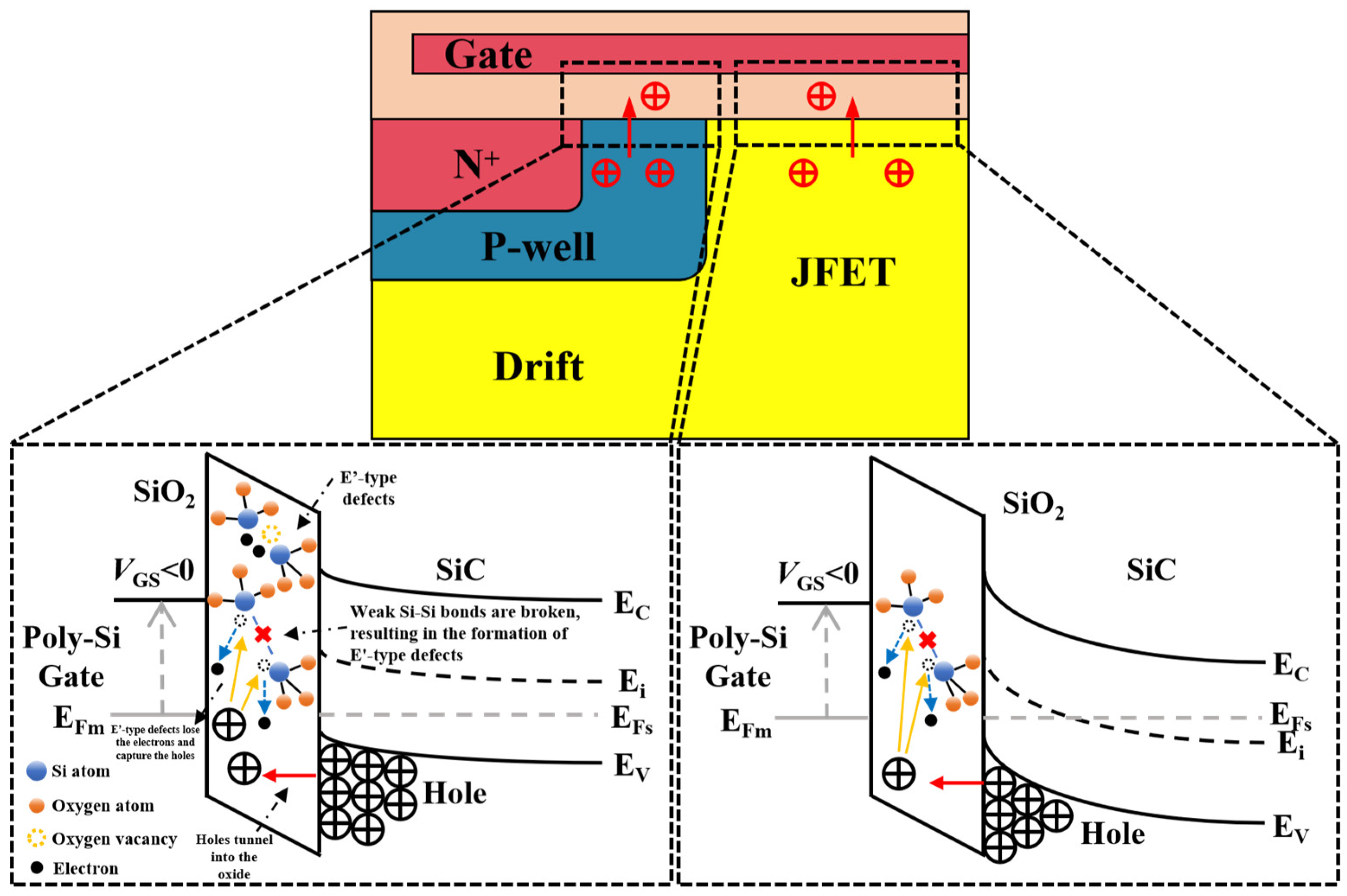
The generation of Qpos in the gate oxide is closely linked to the synergistic interaction between negative gate bias voltage and cyclic high temperature induced by repetitive surge current. Figure 8 shows the energy band diagrams of the gate stack, corresponding to the channel and JFET regions, as well as the process of hole trapping by oxide traps during surge current stress. Under VGS= −5 V, a high density of holes accumulates beneath the oxide layer in the channel and JFET regions. In the energy band diagram, this is manifested by the valence band edge moving closer to the Fermi level, which creates conditions favorable for hole injection into the oxide layer. The surge current can generate a very high instantaneous current density and power density in the active area of the chip, thereby producing a significant amount of Joule heat within the chip. Due to the effects of device thermal resistance and heat capacity, this heat cannot dissipate immediately, leading to a rapid rise in the chip’s junction temperature. At the cell level, under VGS= −5 V, the regions with the highest temperature are primarily the source metal, the gate region, and the body diode. Driven by the gate electric field and the high temperature, holes located at the bottom of the oxide layer can enter the oxide via a tunneling mechanism and become trapped by pre-existing hole traps within the oxide, rendering the traps positively charged. These hole traps belong to near-interfacial oxide defects associated with oxygen vacancies, known as E’-type defects. Structurally, an E’-type defect is characterized by a silicon dangling bond, where a silicon atom bonded to three oxygen atoms hosts an unpaired electron. The high temperature generated by the surge not only promotes hole injection, but also provides activation energy, causing the breaking of certain weak Si-Si bonds (precursors to E’-type defects) within the oxide. These bonds can also be broken during the hole trapping process. This leads to an increase in E’-type defects, which can, in turn, trap more holes [28,29,30]. Finally, under repetitive surge current cycles, the aforementioned process occurs continuously. This results in the continuous generation of new defects, enabling the trapping of an increasing number of holes, and ultimately leading to the continuous accumulation of Qpos. This subsequently drives the degradation of VTH, CGS, and CGD, ultimately causing drift in the device’s switching times and switching losses.

4. Conclusions

This study investigates the degradation behavior and physical mechanisms of switching characteristics in planar-gate SiC MOSFETs under repetitive surge current. Experimental results demonstrate that after 4000 surge current cycles, the turn-on process remains largely unchanged, with no significant variations in td(on), tr, or EON. Conversely, the turn-off process exhibits significant delays, with td(off), tf, and EOFF increasing by 9%, 7.5%, and 8.3%, respectively. The primary factors driving these changes in switching characteristics are the reduction in VTH and the increase in CGS and CGD. The decrease in VTH and increase in CGS result from the accumulation of Qpos within the gate oxide overlying the channel region. Similarly, the increase in CGD stems from Qpos accumulation in the gate oxide overlying the JFET region. These conclusions are experimentally validated by the leftward shift of C-V characteristic curves with increasing cycle counts. The accumulation of Qpos in the gate oxide arises from the combined effects of negative gate bias and cyclic high temperature induced by repetitive surge current. The negative gate bias induces hole accumulation beneath the oxide layer. Assisted by the gate electric field and the elevated junction temperature, these holes enter the oxide via a tunneling mechanism and become trapped by hole traps, specifically E’-type defects. Simultaneously, the high temperature and the hole trapping process can activate more of such defects, thereby enabling the oxide layer to capture more holes. As the number of cycles increases, the oxide layer is continuously subjected to the influence of the gate electric field and high temperature, causing the processes of hole trapping and trap generation to proceed continuously and leading to the accumulation of Qpos. This process triggers the degradation of VTH, CGS, and CGD, and ultimately results in nearly unchanged turn-on time and turn-on loss, but increased turn-off time and turn-off loss of the device. This study not only deepens the understanding of the impact of surge current on devices, but also lays a preliminary foundation for lifetime assessment under repetitive surge current stress. In the future, testing will be conducted at multiple stress levels (e.g., varying surge current magnitudes and temperatures) to gather sufficient data for establishing a more accurate lifetime model.

Author Contributions

Conceptualization, Z.C., L.S., and P.C.; methodology, Z.C. and L.S.; software, Z.C.; validation, Z.C., L.S., and Y.H.; formal analysis, Z.C.; investigation, Z.C. and Y.H.; resources, L.S., F.H., Z.L., and R.J.; data curation, Z.C.; writing—original draft preparation, Z.C.; writing—review and editing, L.S., F.H., Z.L., R.J., and P.C.; visualization, Z.C.; supervision, Z.L. and R.J.; project administration, Z.L. and R.J.; funding acquisition, L.S. All authors have read and agreed to the published version of the manuscript.

Funding

This research was funded by the Program of Beijing Huairou Laboratory, grant number ZD2022004A.

Data Availability Statement

The original contributions presented in this study are included in the article. Further inquiries can be directed to the corresponding author.

Conflicts of Interest

The authors declare no conflicts of interest.

References

  1. She, X.; Huang, A.Q.; Lucía, Ó.; Ozpineci, B. Review of silicon carbide power devices and their applications. IEEE Trans. Ind. Electron. 2017, 64, 8193–8205. [Google Scholar] [CrossRef]
  2. Buffolo, M.; Favero, D.; Marcuzzi, A.; De Santi, C.; Meneghesso, G.; Zanoni, E.; Meneghini, M. Review and outlook on GaN and SiC power devices: Industrial state-of-the-art, applications, and perspectives. IEEE Trans. Electron. Devices 2024, 71, 1344–1355. [Google Scholar] [CrossRef]
  3. Pu, S.; Yang, F.; Vankayalapati, B.T.; Akin, B. Aging mechanisms and accelerated lifetime tests for SiC MOSFETs: An overview. IEEE J. Emerg. Sel. Top. Power Electron. 2022, 10, 1232–1254. [Google Scholar] [CrossRef]
  4. Zhou, W.; Zhong, X.; Sheng, K. High temperature stability and the performance degradation of SiC MOSFETs. IEEE Trans. Power Electron. 2014, 29, 2329–2337. [Google Scholar] [CrossRef]
  5. Górecki, K.; Górecki, P. Selecting operating conditions of power MOSFETs in a power cycling test based on thermal time constants. Energies 2025, 18, 6368. [Google Scholar] [CrossRef]
  6. Górecki, P.; Pietruszka, A.; Skwarek, A.; Illés, B. Reliability tests of the surface-mounted power MOSFETs soldered using SAC0307-TiO2 composite solder paste. In Proceedings of the 2023 29th International Workshop on Thermal Investigations of ICs and Systems (THERMINIC), Budapest, Hungary, 27–29 September 2023. [Google Scholar] [CrossRef]
  7. Bakran, M.M.; Eckel, H.G.; Helsper, M.; Nagel, A. Next generation of IGBT-modules applied to high power traction. In Proceedings of the 2007 European Conference on Power Electronics and Applications, Aalborg, Denmark, 2–5 September 2007. [Google Scholar] [CrossRef]
  8. Sadik, D.P.; Heinig, S.; Jacobs, K.; Johannesson, D.; Lim, J.K.; Nawaz, M.; Dijkhuizen, F.; Bakowski, M.; Norrga, S.; Nee, H.P. Investigation of the surge current capability of the body diode of SiC MOSFETs for HVDC applications. In Proceedings of the 2016 18th European Conference on Power Electronics and Applications (EPE’16 ECCE Europe), Karlsruhe, Germany, 5–9 September 2016. [Google Scholar] [CrossRef]
  9. Gleissner, M.; Bakran, M.M. Surge current protection for railway traction applications. In Proceedings of the 2022 24th European Conference on Power Electronics and Applications (EPE’22 ECCE Europe), Hanover, Germany, 5–9 September 2022. [Google Scholar]
  10. Wang, N.; Zhang, J.; Zhang, Y.; Xu, S.; Deng, F. Evaluation of silicon carbide power MOSFET on third-quadrant surge current performance. In Proceedings of the IECON 2025—51st Annual Conference of the IEEE Industrial Electronics Society, Madrid, Spain, 14–17 October 2025. [Google Scholar] [CrossRef]
  11. Soeiro, T.B.; Mengotti, E.; Bianda, E.; Ortiz, G. Performance evaluation of the body-diode of SiC MOSFETs under repetitive surge current operation. In Proceedings of the IECON 2019—45th Annual Conference of the IEEE Industrial Electronics Society, Lisbon, Portugal, 14–17 October 2019. [Google Scholar] [CrossRef]
  12. Awwad, A.E.; Dieckerhoff, S. Operation of planar and trench SiC MOSFETs in a 10 kW DC/DC-converter analyzing the impact of the body diode. In Proceedings of the 2017 IEEE Energy Conversion Congress and Exposition (ECCE), Cincinnati, OH, USA, 1–5 October 2017. [Google Scholar] [CrossRef]
  13. Yamaguchi, K.; Katsura, K.; Yamada, T.; Sato, Y. Criteria for using antiparallel SiC SBDs with SiC MOSFETs for SiC-based inverters. IEEE Trans. Power Electron. 2020, 35, 619–629. [Google Scholar] [CrossRef]
  14. Ma, D.; He, Z.; Chen, Y.; Shi, Y.; Wang, J.; Yang, C.; Zhang, M.; Shen, Y.; He, L.; Lu, G.; et al. Degradation evaluation and defects analysis for 1.2-kV planar-gate SiC MOSFETs under repetitive surge current stress. IEEE Trans. Electron. Devices 2023, 70, 6473–6479. [Google Scholar] [CrossRef]
  15. Zhu, Z.; Ren, N.; Xu, H.; Liu, L.; Guo, Q.; Zhang, J.; Sheng, K.; Wang, Z. Degradation of 4H-SiC MOSFET body diode under repetitive surge current stress. In Proceedings of the 2020 32nd International Symposium on Power Semiconductor Devices and ICs (ISPSD), Vienna, Austria, 13–18 September 2020. [Google Scholar] [CrossRef]
  16. Jiang, X.; Wang, J.; Chen, J.; Li, Z.; Zhai, D.; Yang, X.; Ji, B.; Shen, Z.J. Investigation on degradation of SiC MOSFET under surge current stress of body diode. IEEE J. Emerg. Sel. Top. Power Electron. 2020, 8, 77–89. [Google Scholar] [CrossRef]
  17. Wang, Z.; Li, Y.; Sun, X.; Liu, Y.; Zhu, Z.; Ren, N.; Guo, Q. Reliability investigation on SiC trench MOSFET under repetitive surge current stress of body diode. In Proceedings of the 2020 IEEE Workshop on Wide Bandgap Power Devices and Applications in Asia (WiPDA Asia), Suita, Japan, 23–25 September 2020. [Google Scholar] [CrossRef]
  18. Zhan, X.; He, Y.; Xia, T.; Yuan, S.; Yuan, H.; Song, Q. Degradation evaluation for ion implantation doping in 1.2 kV SiC MOSFET body diode under third quadrant conduction. IEEE J. Emerg. Sel. Top. Power Electron. 2026, 14, 2049–2057. [Google Scholar] [CrossRef]
  19. Wei, J.; Liu, S.; Ye, R.; Chen, X.; Song, H.; Sun, W.; Su, W.; Ma, S.; Liu, Y.; Lin, F.; et al. Interfacial damage extraction method for SiC power MOSFETs based on C-V characteristics. In Proceedings of the 2017 29th International Symposium on Power Semiconductor Devices and IC’s (ISPSD), Sapporo, Japan, 28 May–1 June 2017. [Google Scholar] [CrossRef]
  20. IEC 60747-8; Semiconductor Devices—Discrete Devices—Part 8: Field-Effect Transistors. IEC: Geneva, Switzerland, 2021.
  21. Baliga, B.J. Fundamentals of Power Semiconductor Devices, 2nd ed.; Springer: Cham, Switzerland, 2019; pp. 443–448. [Google Scholar]
  22. Power MOSFET Basics: Understanding Gate Charge and Using it to Assess Switching Performance. Available online: https://www.vishay.com/docs/73217/an608a.pdf (accessed on 16 February 2016).
  23. Yang, X.; Wang, X.; Li, Q.; Liu, Y.; Sun, Y.; Liu, G. An accurate datasheet-driven analytical model of SiC MOSFET incorporating stage-dominant Cgs (Vgs, Vds) and Cgd (Vgs, Vds). IEEE Trans. Power Electron. 2026, 1–16. [Google Scholar] [CrossRef]
  24. Wei, J.; Liu, S.; Yang, L.; Fang, J.; Li, T.; Li, S.; Sun, W. Comprehensive analysis of electrical parameters degradations for SiC power MOSFETs under repetitive short-circuit stress. IEEE Trans. Electron. Devices 2018, 65, 5440–5447. [Google Scholar] [CrossRef]
  25. Cai, Y.; Sun, P.; Chen, C.; Zhang, Y.; Zhao, Z.; Li, X.; Qi, L.; Chen, Z.; Nee, H.P. Investigation on gate oxide degradation of SiC MOSFET in switching operation. IEEE Trans. Power Electron. 2024, 39, 9565–9578. [Google Scholar] [CrossRef]
  26. Wang, Z.; Yang, F.; Campbell, S.L.; Chinthavali, M. Characterization of SiC trench MOSFETs in a low-inductance power module package. IEEE Trans. Ind. Appl. 2019, 55, 4157–4166. [Google Scholar] [CrossRef]
  27. Cai, Y.; Chen, C.; Zhao, Z.; Sun, P.; Li, X.; Zhang, M.; Wang, H.; Chen, Z.; Nee, H.P. Characterization of gate-oxide degradation location for SiC MOSFETs based on the split C-V method under bias temperature instability conditions. IEEE Trans. Power Electron. 2023, 38, 6081–6093. [Google Scholar] [CrossRef]
  28. Lelis, A.J.; Green, R.; Habersat, D.B.; El, M. Basic mechanisms of threshold-voltage instability and implications for reliability testing of SiC MOSFETs. IEEE Trans. Electron. Devices 2015, 62, 316–323. [Google Scholar] [CrossRef]
  29. Lelis, A.J.; Green, R.; Habersat, D.B. (Invited) Effect of threshold-voltage instability on SiC power MOSFET high-temperature reliability. ECS Trans. 2011, 41, 203–214. [Google Scholar] [CrossRef]
  30. Lelis, A.J.; Green, R.; Habersat, D.B. High-temperature reliability of SiC Power MOSFETs. Mater. Sci. Forum 2011, 679, 599–602. [Google Scholar] [CrossRef]
Figure 1. (a) Repetitive surge current test platform; (b) measured source-drain current (ISD) and voltage (VSD) during a surge event; (c) circuit schematic and (d) physical photograph of the double-pulse test setup, showing the printed circuit board (PCB) layout.
Electronics 15 02721 g001
Figure 2. Evolution of the (a) turn-on and (b) turn-off processes of the device under test (DUT) under an increasing number of surge current cycles.
Electronics 15 02721 g002
Figure 3. Switching times of the DUT as a function of surge current cycles, including (a) turn-on time (ton), turn-on delay time (td(on)), and rise time (tr); and (b) turn-off time (toff), turn-off delay time (td(off)), and fall time (tf).
Electronics 15 02721 g003
Figure 6. The evolution of (a) transfer characteristics curve, (b) gate-source capacitance (CGS)-drain-source voltage (VDS) curve, and (c) gate-drain capacitance (CGD)-VDS curve with increasing surge current cycles. The inset in (a) displays the change in threshold voltage (ΔVTH) as a function of cycle number.
Electronics 15 02721 g006
Figure 7. Capacitance-voltage (C-V) characteristic curves of the DUT under different numbers of surge current cycles. The measured capacitance is the input capacitance Ciss of the device, which is the sum of the CGS and CGD. During the measurement, the voltage is applied between the gate and source terminals.
Electronics 15 02721 g007
Figure 8. Energy band diagrams of the gate stack structure over the channel and JFET region in the planar-gate SiC MOSFET under negative gate bias voltage, as well as the process of holes being trapped by oxide traps during surge current stress.
Electronics 15 02721 g008
Disclaimer/Publisher’s Note: The statements, opinions and data contained in all publications are solely those of the individual author(s) and contributor(s) and not of MDPI and/or the editor(s). MDPI and/or the editor(s) disclaim responsibility for any injury to people or property resulting from any ideas, methods, instructions or products referred to in the content.