1. Introduction
Wide-bandgap (WBG) semiconductor devices, especially silicon carbide (SiC) MOSFETs, have enabled compact and high-efficiency power converters. Owing to their much higher critical electric field, SiC devices achieve a dramatically lower specific on-resistance than silicon counterparts, while simultaneously supporting higher current ratings and faster switching transients. These characteristics make SiC MOSFETs attractive replacements for traditional Si IGBTs in applications that demand high switching frequencies and improved energy efficiency.
However, in most high-power systems, such as EV traction inverters, photovoltaic inverters, and DC fast chargers, the achievable switching speed of SiC MOSFETs is often limited not by the device itself but by the parasitic elements of the power module. Conventional wire-bonded packages on direct-bonded copper (DBC) substrates exhibit relatively large commutation and gate-loop inductances due to their long wire interconnects and bulky ceramic structures [
1]. These parasitics introduce several challenges when used with fast SiC devices. The combination of a large gate-loop inductance and the intrinsically low input capacitance of SiC MOSFETs can cause substantial gate-voltage ringing, necessitating a higher gate resistance to maintain stability. Likewise, excessive power-loop inductance leads to increased switching losses, elevated voltage overshoot during turn-off, and potentially unsafe device stress at high di/dt. As a result, designers are often forced to deliberately slow down switching transitions to maintain reliability and comply with EMI constraints [
2], thereby compromising the performance advantages that SiC technology inherently offers.
On the other hand, as the system power level scales up, parallel operation of multiple half-bridge modules becomes essential, yet this introduces new challenges in current balancing and electromagnetic interference (EMI). Conventional packaging structures, such as DBC-based, press-fit, and wire-bonded half-bridge modules, are inherently unfavorable for parallel operation. Their long bond wires, significant bulky volume, vertical construction, and asymmetric busbar layout cause parasitic mismatches, resulting in unequal current sharing, increased switching loss, and unbalanced thermal stress [
3,
4]. These challenges limit the current SiC packaging technologies’ capability in high-power, high-speed applications.
Given these limitations, there is a clear need for new packaging approaches that can better exploit the fast-switching capability of SiC MOSFETs. Several alternatives have been investigated in recent years, including wireless-interconnection structures and printed-circuit-board (PCB)-embedded modules [
5,
6,
7,
8]. The wireless-interconnection concept often struggles to support adaptable bonding configurations and device layouts, which restricts its practical applicability. On the other hand, PCB-embedded solutions are particularly attractive because their highly compact geometry can minimize parasitic inductance and resistance [
9,
10,
11,
12]. Nevertheless, their adoption in commercial products has been limited, partly due to the higher fabrication cost and the need for specialized processing.
To overcome these challenges, this work introduces a new ultra-compact SiC MOSFET half-bridge module based on a die-integrated 3D PCB package architecture. The proposed design eliminates conventional wire bonds by employing PCB copper planes as integrated busbars, enabling a low-inductance and fully manufacturable interconnection scheme. The module is realized by vertically stacking multiple PCBs with the SiC dies embedded between them, forming a compact and symmetric structure. This arrangement not only reduces the overall size and mass of the module [
13,
14,
15] but also provides highly consistent parasitic characteristics across modules, making it particularly well suited for parallel operation in high-power applications.
This paper provides a comprehensive description and evaluation of the proposed die-integrated PCB-based SiC MOSFET half-bridge module.
Section 2 outlines the overall packaging architecture and the fabrication procedure.
Section 3 presents the module’s static characteristics, including the I-V behavior and high-voltage insulation performance.
Section 4 examines the thermal behavior through a combination of numerical simulation and experimental measurements.
Section 5 reports the extraction of parasitic parameters using finite-element electromagnetic modeling.
Section 6 discusses the inherent benefits of the proposed structure when multiple modules are operated in parallel.
Section 7 analyzes the dynamic performance of the module through double-pulse testing and switching characterization.
2. Proposed Die-Integrated PCB SiC MOSFET Half-Bridge Building Block
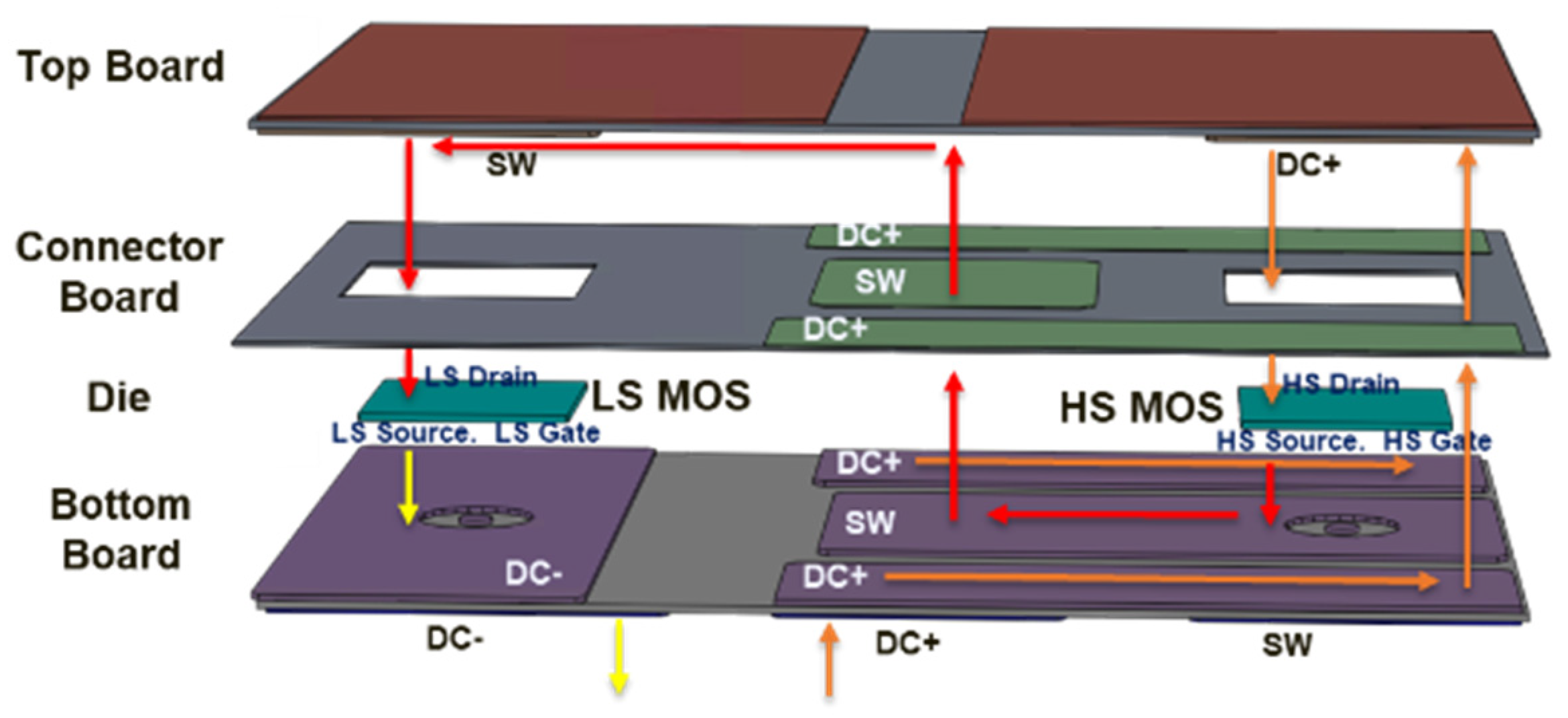
The exploded 3D view of the proposed die-integrated PCB half-bridge module is illustrated in
Figure 1. It consists of three PCBs, as shown in
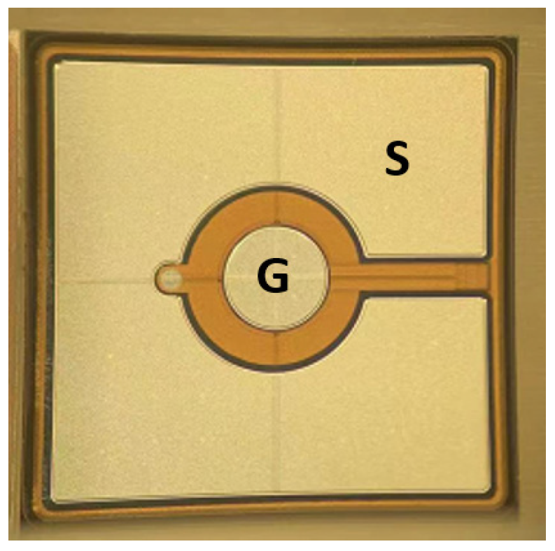
Figure 2. Two 1200 V/13.8 mΩ double-sided solderable SiC MOSFET dies from Onsemi, as presented in
Figure 3, are sandwiched between the top and the bottom boards. The arrows indicate the current flow directions during the switching operation. Different colors represent the copper planes across the stacked PCB layers. For balanced thermal performance, the two dies are symmetric from top to bottom. The bottom surface of the module is the electrical connection side and is solderable for surface mount assembly to form the final circuit. The top surface of the module is the heat sink side, with a flat, exposed copper surface for improved heat dissipation. Single-sided cooling was selected to preserve the low-inductance laminated bus structure. However, the PCB-embedded approach is compatible with double-sided cooling by adopting metal-core substrates or high-density thermal vias.
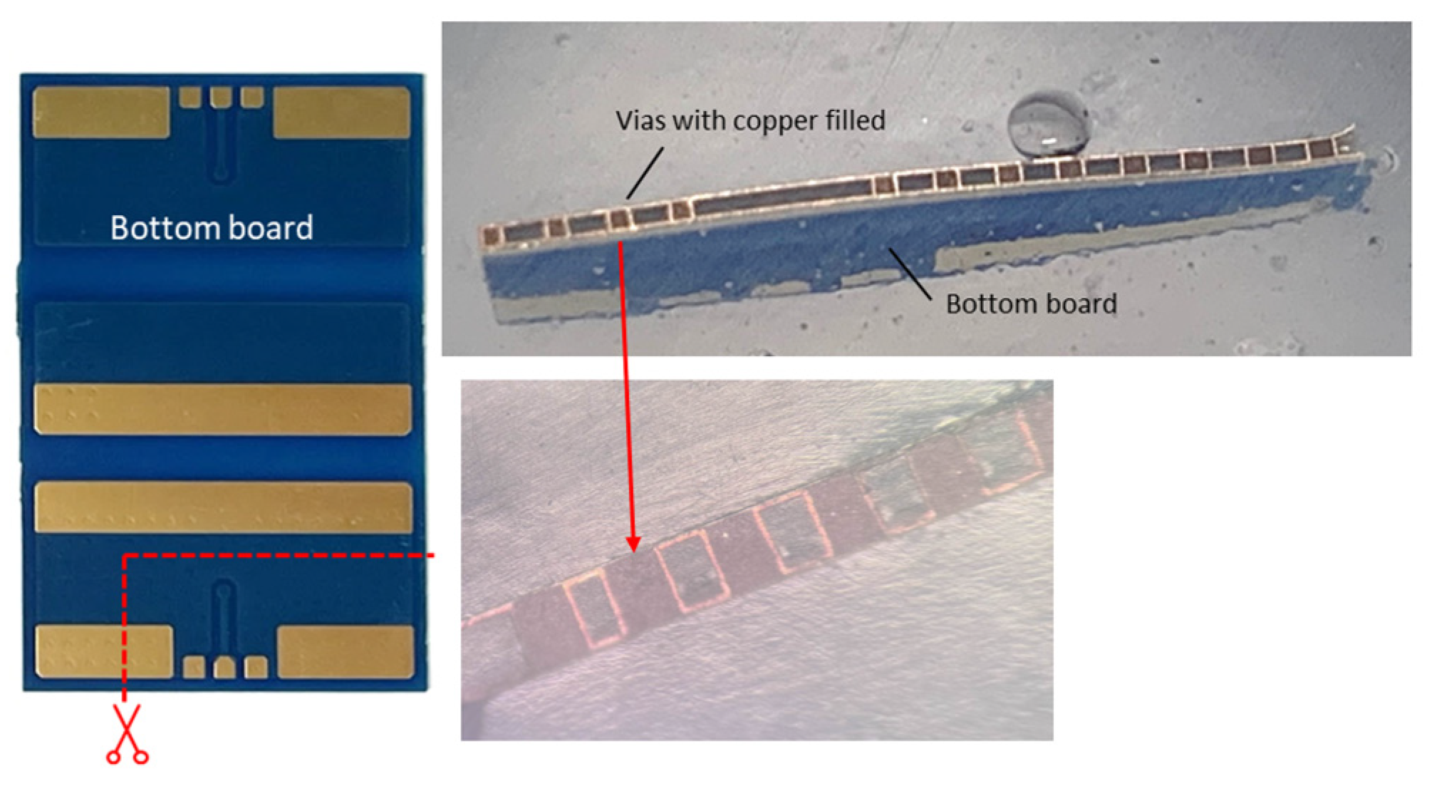
Copper-filled vias are used on the top and bottom boards to reduce package resistance and improve cooling performance, as shown in
Figure 4. The arrows show the mapping between the bottom-board layout and the cross-sectional image. The dashed region denotes the inspected area, and the scissor symbol represents the sectioning location. The connector board, with the same thickness as the SiC MOSFET die, is used for connections and alignment. With this packaging approach, the module’s total loop is minimized, and the fabrication process is simplified. The power loop in the module is horizontally symmetric to achieve flux cancellation, hence minimizing the power loop inductance. The standard soldering process assembles all parts.
Due to the symmetric copper-die-copper structure, mechanical stress during thermal cycling is minimized. In addition, the proposed structure is compatible with high glass transition temperature (Tg) (>190 °C) laminates commonly used for high-temperature power modules, suggesting the feasibility of continuous operation at 175 °C with appropriate material selection [
9].
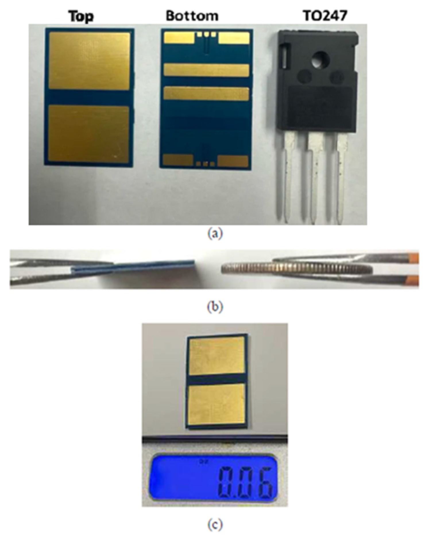
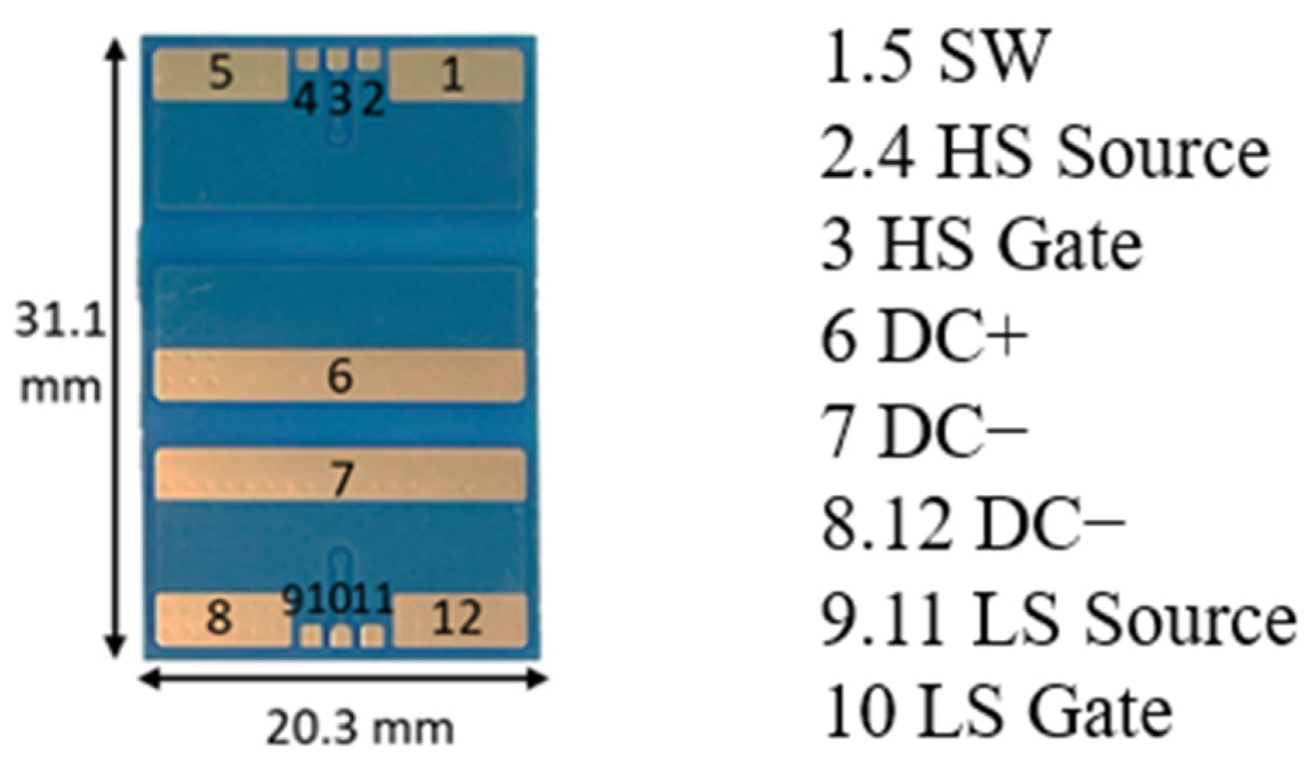
The packaged module has dimensions of 20.3 mm × 31.1 mm × 1.0 mm and weighs only 0.06 oz, as shown in
Figure 5c. The top and bottom views of the actual half-bridge module are demonstrated in
Figure 5a, with a comparison to a TO-247 package. And the module thickness is compared with a quarter coin in
Figure 5b. The module pin arrangement is shown in
Figure 6. Multiple modules could be placed in parallel to achieve higher current levels. The DC+ and DC− terminals are placed in the middle of the module to minimize power-loop inductance, whereas the SW terminal is on one side. Independent gate and source pins are reserved for Kelvin gate-driver connections for the high-side (HS) and low-side (LS) MOSFETs. Compare a similar (voltage and on-resistance) half-bridge module from Cree [
13]. The active area is more than 2.5 times the size of the proposed module. The specifications of the developed half-bridge building block module are summarized in
Table 1.
3. Static Characteristics
3.1. I-V Characteristic and Package Resistance
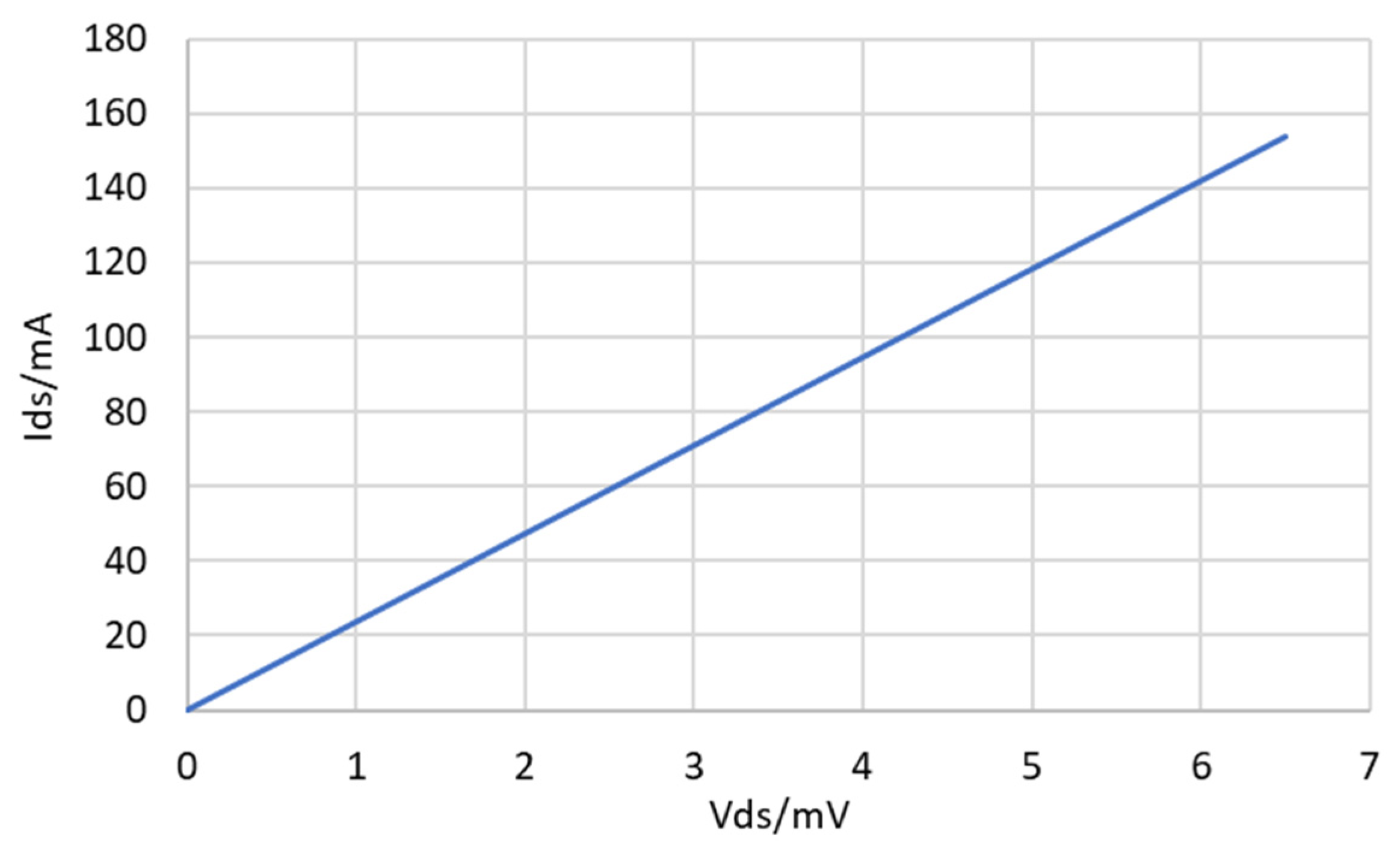
Figure 7 presents the measured I-V curve of the low-side MOSFET in the proposed module at Vgs = 18 V and room temperature, measured with a Tektronix 370 A Curve Tracer. It indicates that the R
ds,on is 17 mΩ at this condition, with 3.2 mΩ from the package and soldering. The detailed analysis of the parasitic resistance is discussed in
Section 5.
3.2. Insulation Performance
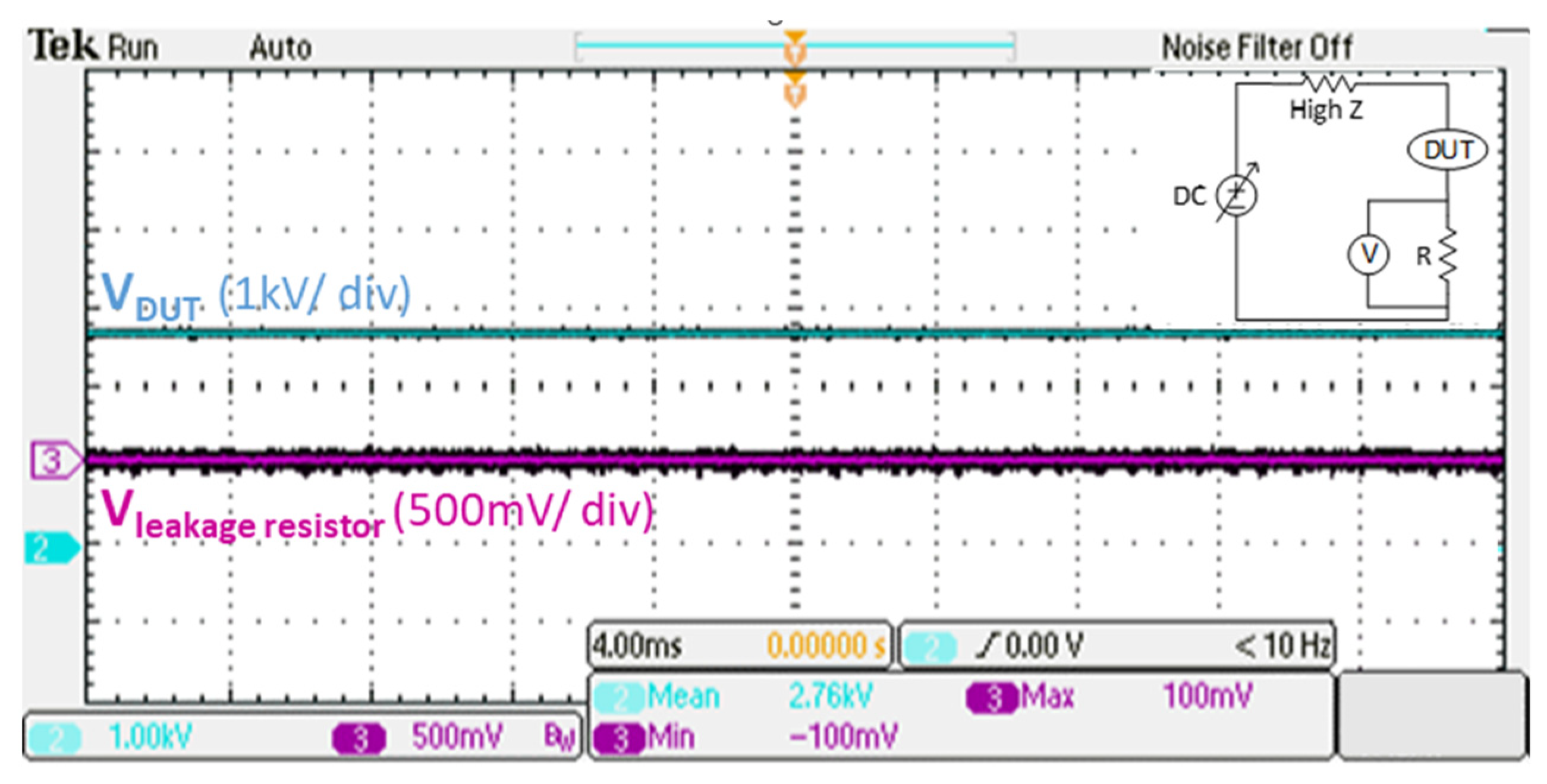
The High-Pot test (High-Potential Test) is performed to verify the insulation capability of the proposed module package. PCB dummy dies with the same thickness and size as the SiC MOSFET dies are soldered inside the half-bridge building block module to replace the SiC MOSFET dies as the device under test (DUT). The DUT and two external resistors are connected in series with a DC power supply. One high-impedance resistor is also in series in the test circuit for circuit protection, and the other is a low-impedance resistor for leakage current observation. The High-Pot test result of the DC+ to DC− terminals is shown in
Figure 8. This test applies the high voltage for 5 min. No failure or high leakage current is observed with 2.76 kV applied between the DC+-to-DC− terminals in air, which is over 2.5 times the module voltage rating.
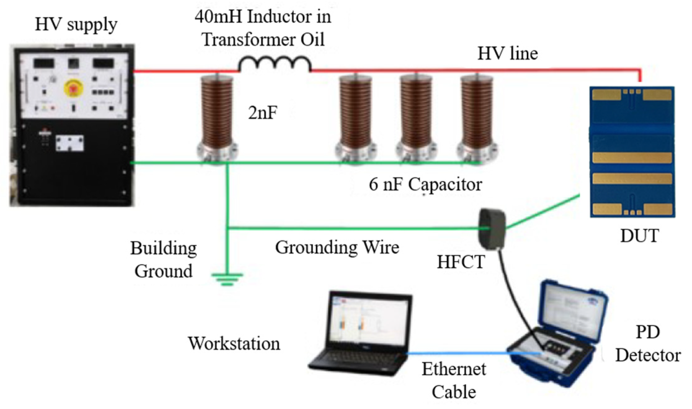
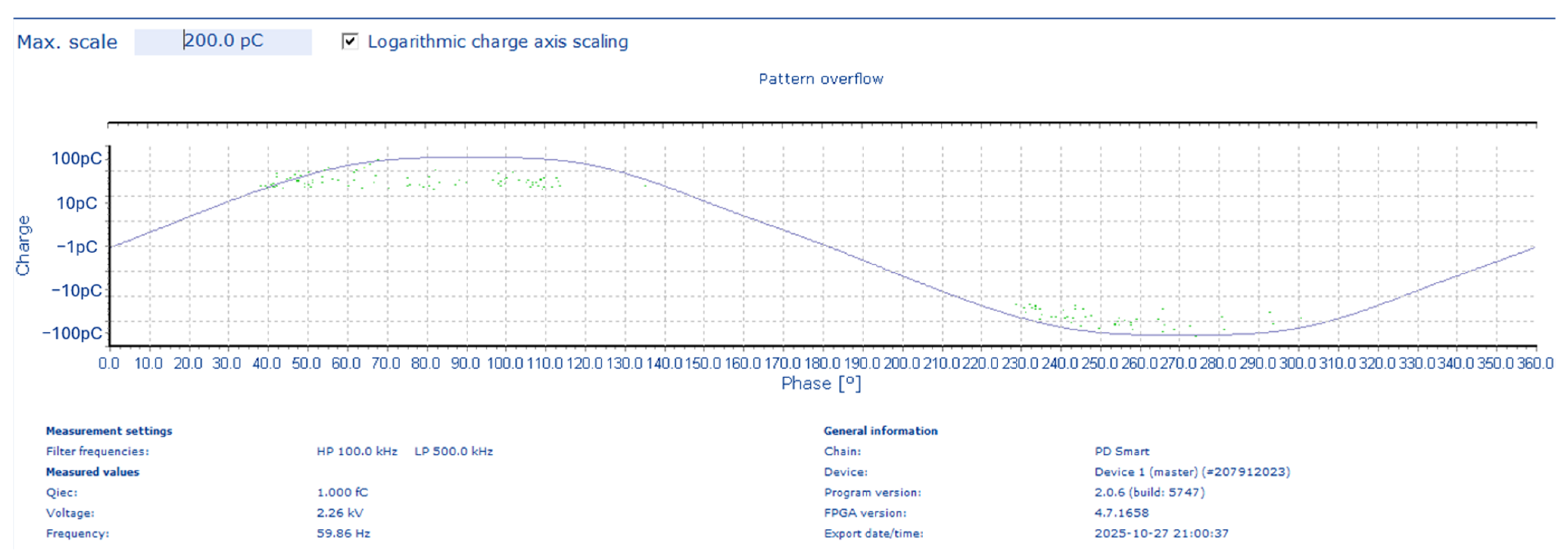
To evaluate the isolation behavior of the proposed module under sinusoidal high voltage stress, Partial Discharge (PD) measurements were carried out using the setup shown in
Figure 9. A high-frequency current transformer (HFCT) was employed to detect the PD impulse current, while a C-L-3C filter was implemented to suppress the PD-like noise generated by the power supply. With all external connections properly terminated, the setup supports both AC and DC PD testing up to 30 kV, achieving a background noise level of approximately 5 pC [
16].
Figure 10 shows the pattern diagram of the PD test under 60 Hz AC excitation, and the measured partial discharge inception voltage (PDIV) for the proposed package from the DC+ terminal to the DC− terminal is approximately 2 kVrms/(≈2.828 kV peak) in air, representing an averaged value over multiple measurements and exceeding twice the device rated bus voltage.
Figure 11 presents the partial discharge record over 1 min. At 60 Hz and 2.26 kVrms, the discharge magnitude remains below 50 pC and appears only intermittently once the applied voltage surpasses the 2 kVrms threshold.
4. Package Thermal Characteristics
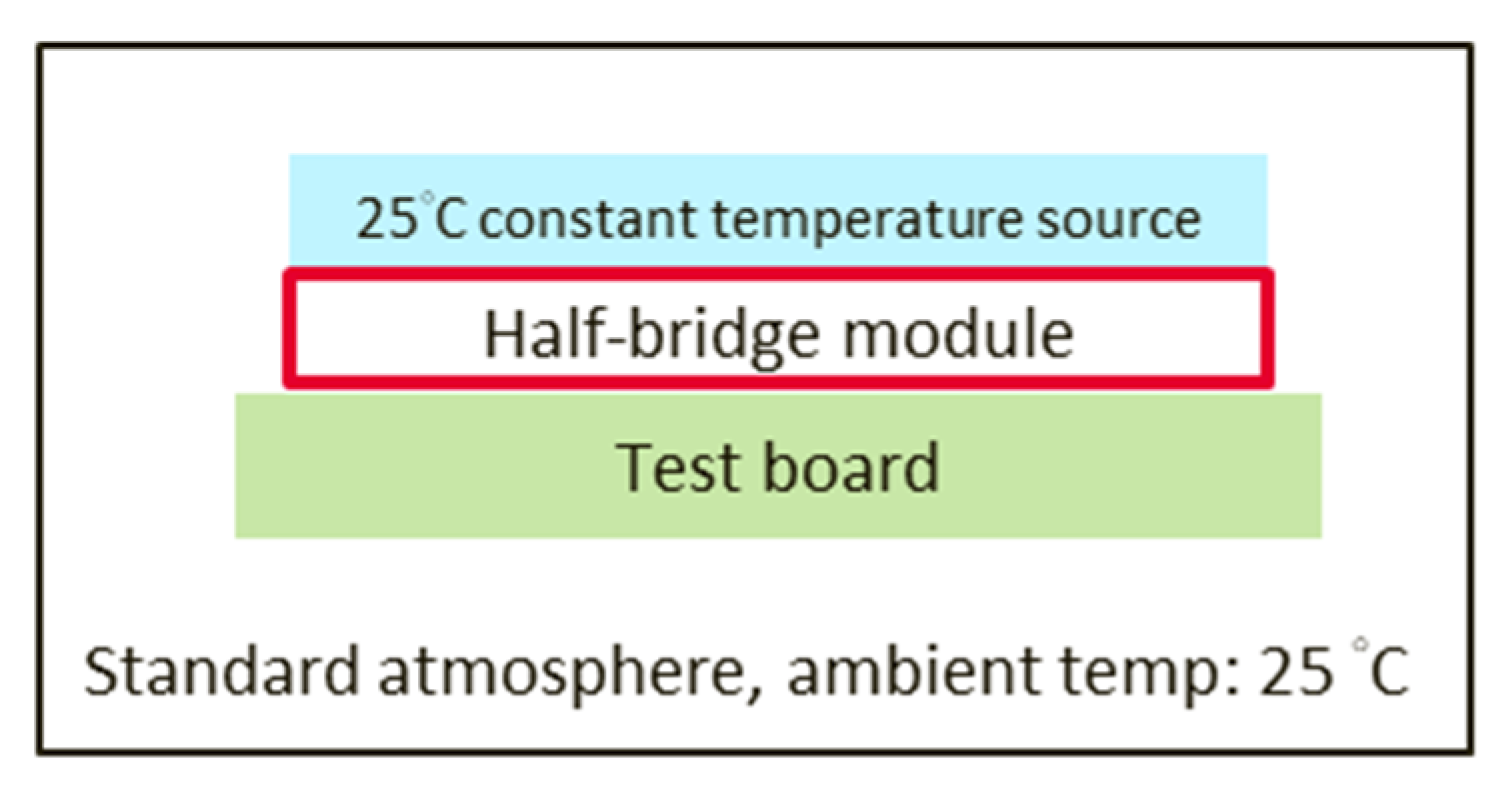
SolidWorks 2023 Flow Simulation analyzes the junction-to-case thermal resistance (θ
JC) of the module. The simulation condition is shown in
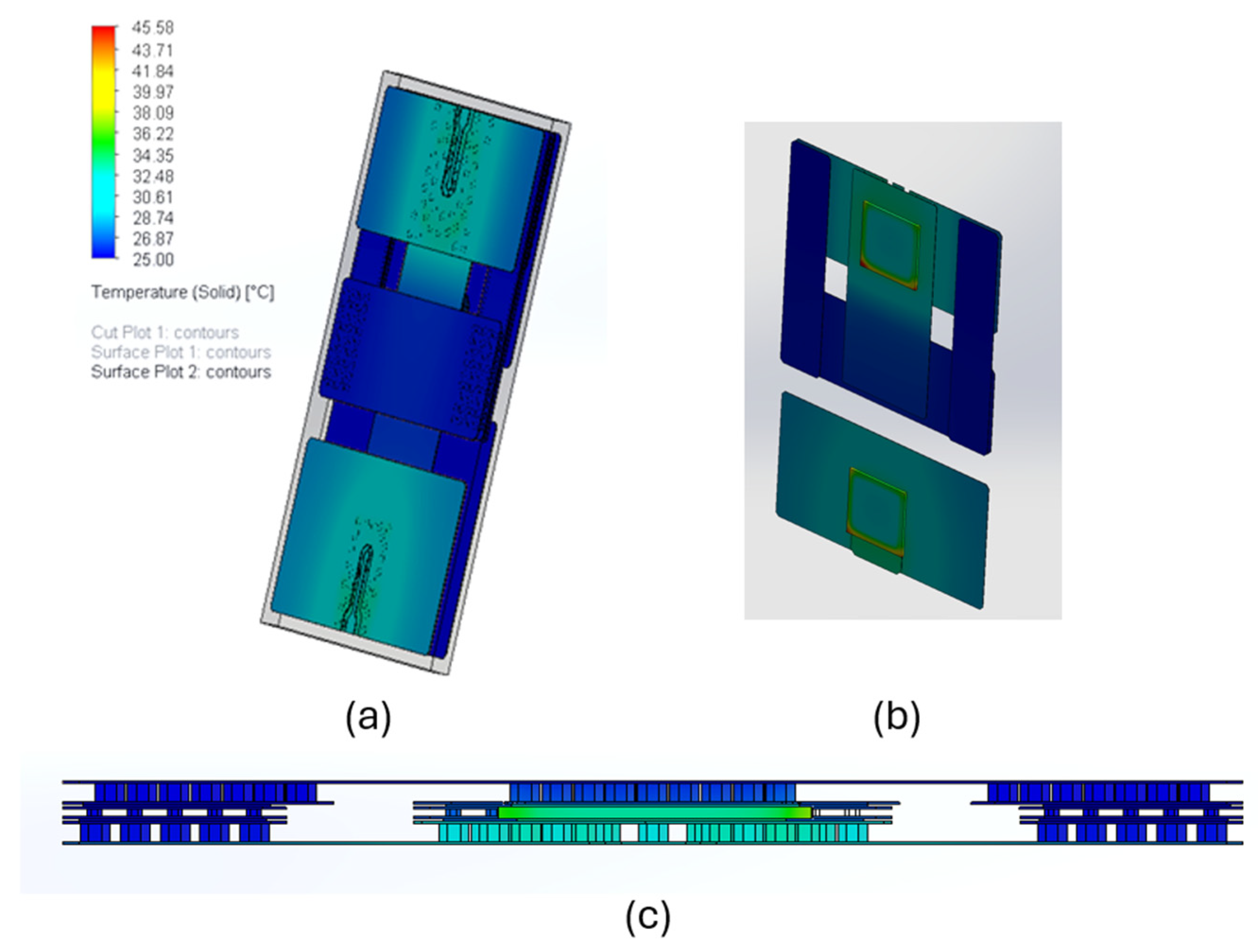
Figure 12. The simulation is run under standard atmospheric conditions with a 25 °C ambient temperature. A model with the same structure as the fabricated module is shown in
Figure 13. A 25 °C constant-temperature boundary condition is applied to the thermal pad on the module’s top surface. The bottom surface of the module is attached to a 1.6 mm-thick FR4 plate, with natural convection, to simulate the actual application conditions. The two SiC MOSFET dies are set as heat sources, each generating 50 W. The simulation result is shown in
Figure 13. The maximum junction temperature is 45.58 °C, yielding a calculated junction-to-case thermal resistance of approximately 0.41 °C/W per device.
The junction-to-case thermal resistance is also verified experimentally. The forward voltage of the SiC MOSFET intrinsic body diode is used as the temperature-sensitive electrical parameter (TSEP) for non-invasive electrical temperature measurement [
17,
18,
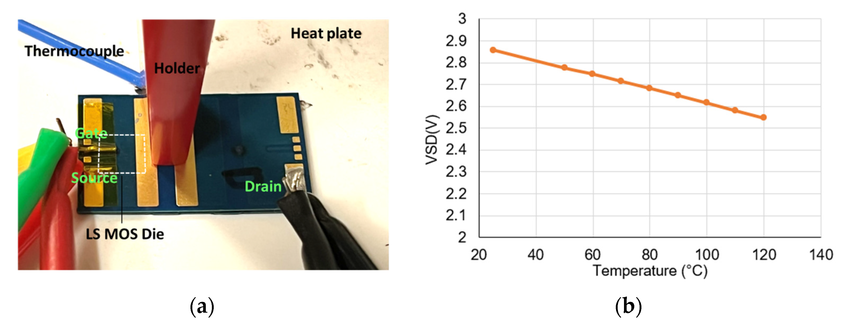
19]. The forward-voltage-to-temperature calibration curve is measured using the setup shown in
Figure 14a. The module’s top surface is placed on a heat plate. Thermocouples are used to monitor the temperature at the bottom surface of the module and the heat plate. Steady state temperature is ensured. Two voltage sources are applied to the LS MOSFET, one on the source-to-drain with a 100 mA constant current to conduct the body diode, and the other on gate-to-source providing −5 V Vgs. The forward-voltage temperature calibration curve is shown in
Figure 14b. The curve is linear with a calculated slope of −3.3 mV/°C.
The junction-to-case thermal resistance of the module is measured at room temperature. The module is heated under the same electrical conditions as the TSEP calibration. The case temperature is monitored with the thermocouple. After thermal reach balance, 36.3 °C is measured on the case. The source-to-drain voltage is measured to be 2.823 V, which corresponds to 36.42 °C at the junction according to the calibrated curve. The power dissipation is 0.282 W. The measured θJC is 0.44 °C/W, which differs from the simulation result by only 0.03 °C/W.
For SiC MOSFET operating at an elevated junction temperature of 175 °C, R
ds,on is 30 mΩ. Based on the simulation and the tested package thermal resistance, the DC current rating of the module is determined by Equation (1)
5. Package Loop Parasitic Parameters Optimization
The power device’s dynamic performance is highly dependent on the power module’s parasitic parameters. The gate loop determines the device’s switching speed, while the power loop influences the overshoot voltage. In the proposed SiC half-bridge module, the power loop has been carefully designed to minimize parasitic loop parameters; in addition, symmetrical power and gate loops enable reliable, scalable parallel operation.
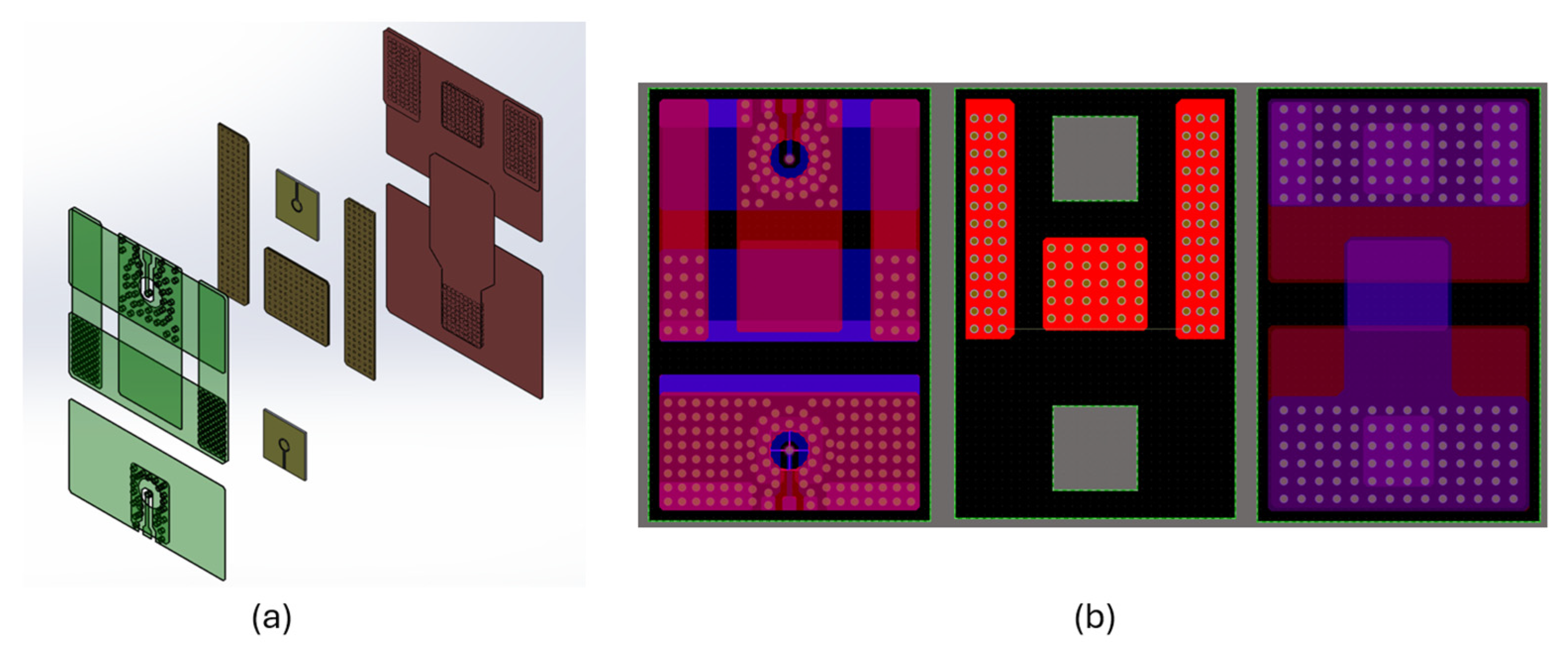
Figure 15 shows the copper layout for the three PCBs. The proposed SiC half-bridge module inherently facilitates parallel operation due to its symmetric planar architecture, consistent parasitic distribution, and compact module footprint. The mirror-imaged current paths in
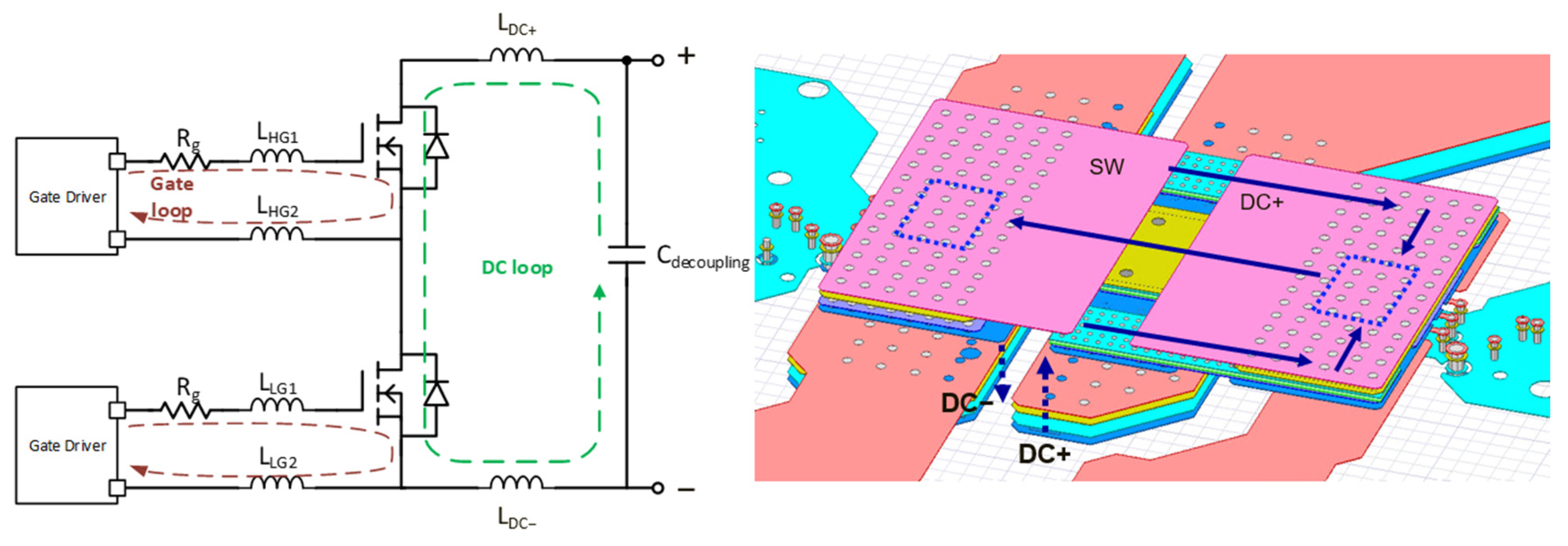
Figure 15 ensure identical power-loop and gate-loop inductances. ANSYS Electronics Desktop 2023 Q3D Extractor is used to extract the parasitic parameters for analysis and optimization during the module design. The module application schematic and the Q3D simulation model for the parasitic gate loop and power are shown in
Figure 16. The dashed arrows in the left plot indicate the gate loop and DC commutation loop, respectively. The arrows in the right plot illustrate the current flow paths during the switching operation. In addition, different colors indicate the multiple copper layers in the laminated PCB structure.
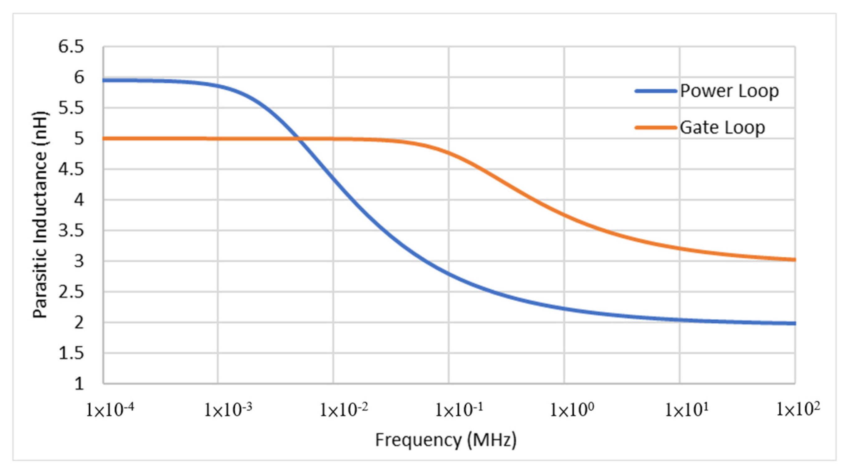
Based on the parasitic loop inductance simulation results over the frequency range shown in
Figure 17, the parasitic inductance of the gate loop is 3.8 nH at 1 MHz. The inductance value is reduced by 89% compared with the TO-247 package half-bridge module [
10]. The parasitic inductance of the power loop is 2.2 nH at 1 MHz, which is 94% lower than that of the TO-247 package half-bridge module.
The parasitic resistances are 12 mΩ for the gate loop and 2.4 mΩ for the power loop at 1 MHz, which can match the I-V measurement in III. A tolerance study was performed by applying ±10% variation to the dielectric spacing and copper thickness. The resulting power loop inductance changed <±5%, demonstrating the weak dependence of loop inductance on vertical layer spacing. Resistance varied from 2.4 mΩ to 2.2–2.6 mΩ due to variations in copper thickness and size. These manufacturing tolerances do not affect the module’s switching behavior.
In high-speed SiC modules, the package capacitance between switching nodes and DC buses forms an unintended common-mode current path. During fast voltage transitions, this capacitance injects displacement currents that can increase EMI, distort the dv/dt balance among paralleled modules, and reduce insulation lifetime. Therefore, achieving a symmetric layout and controlled dielectric spacing in the packaging stack-up is essential to mitigate capacitive coupling while maintaining compactness. Based on the Q3D simulation, the package parasitic capacitance list is shown in
Table 2. The parasitic capacitance between nets is negligible, which is less than 2% of the internal capacitance of the SiC MOSFET.
6. Symmetrical Power Loop and Planar Structure for Parallel
From a mechanical and manufacturing perspective, traditional discrete or DBC modules are bulky, making precise symmetrical routing difficult. Each additional module adds assembly complexity, stray parasitics, and cost. Furthermore, conventional wire-bond interconnects are not well-suited for tightly coupled planar layouts, limiting scalability.
The proposed PCB-embedded half-bridge module is inherently well-suited for parallel operation due to its symmetrical current path layout, planar magnetic-field cancellation, ultra-low parasitic coupling, and ultra-compact package footprint.
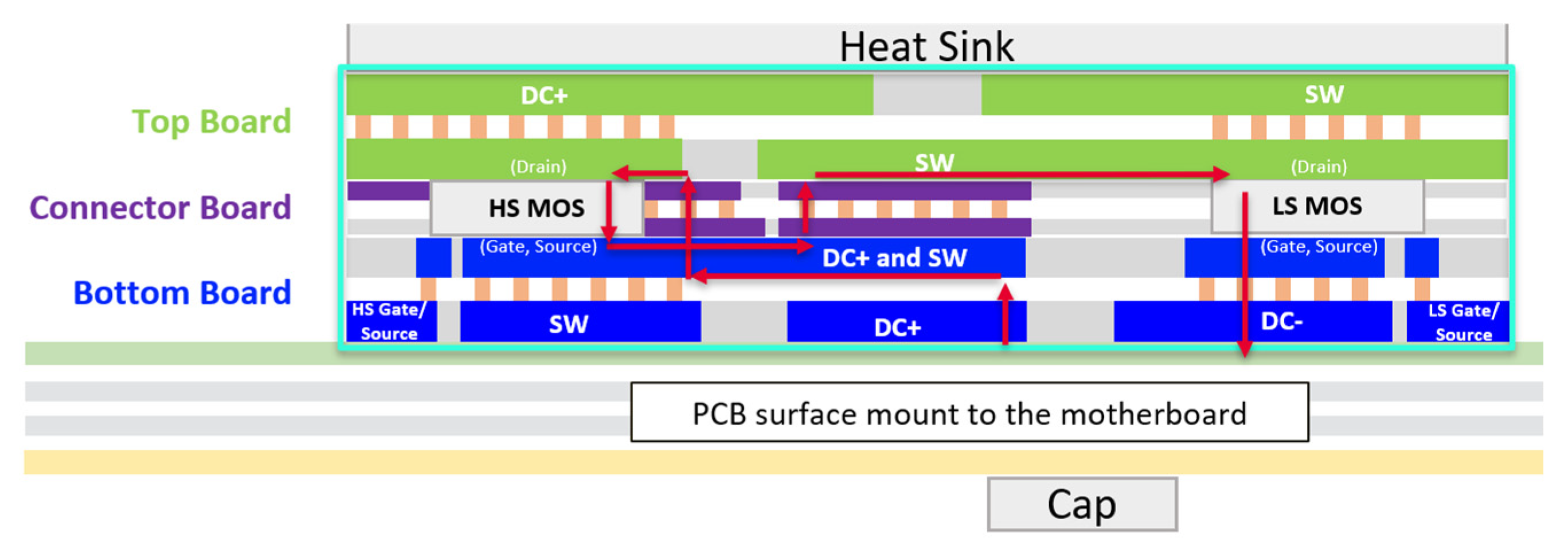
Each module integrates an internal anti-parallel current return path using multilayer copper planes, forming a compact loop that strongly cancels magnetic flux, as shown in
Figure 18, with the cross-sectional view and current direction. The arrows indicate the current flow paths during the switching operation. Different colors indicate the copper layers distributed across the top, connector, and bottom boards. This configuration effectively minimizes the self-loop inductance (≈2.2 nH) while confining the magnetic field within the module boundaries.
When two or more modules are paralleled, their power current directions are identical, yet the internal field confinement ensures that the inter-module magnetic coupling remains very weak.
As a result, the modules are electromagnetically decoupled, eliminating cross-talk and suppressing circulating current during high di/dt switching transitions.
In addition, the planar layout and standard PCB fabrication processes provide equalized DC-link and switching-node impedances across all modules, ensuring that voltage and current transients are shared uniformly. Therefore, the proposed packaging architecture not only achieves minimal parasitic imbalance but also inherently stabilizes current sharing among paralleled SiC modules—without requiring external balancing inductors or complex gate synchronization. This natural equalization effect allows scalable power expansion while maintaining high switching speed, low EMI, and excellent thermal uniformity.
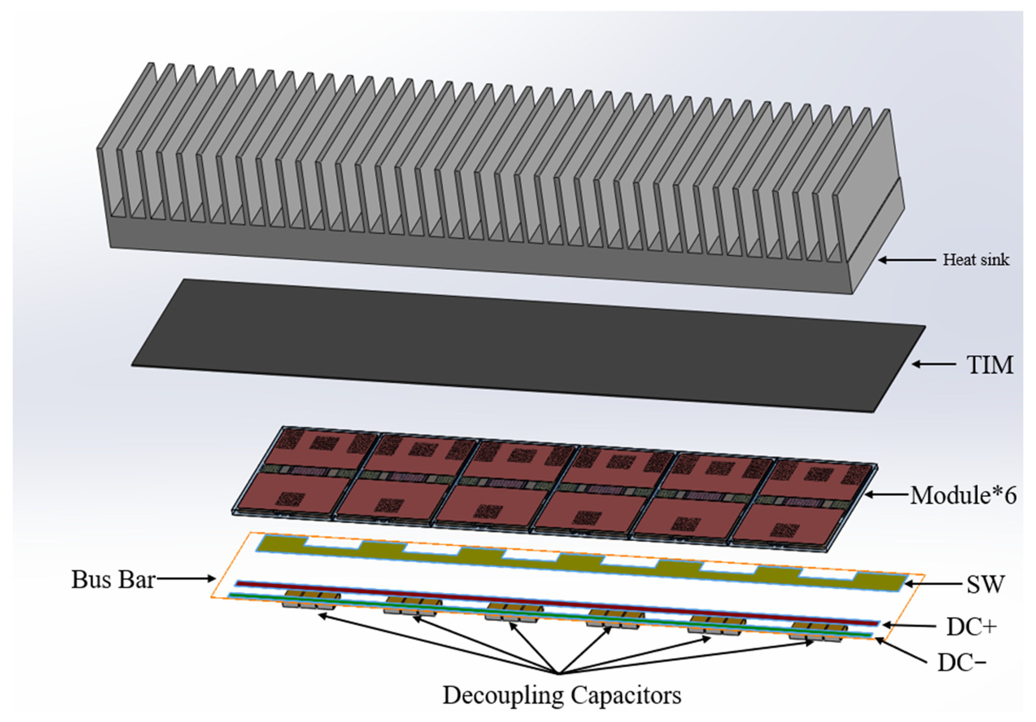
Figure 19 illustrates a six-module parallel architecture for scalable SiC-based converter systems. The modules are mounted side by side on a common planar busbar composed of three copper layers (DC+, SW, and DC−).
This bus structure ensures identical electrical and geometric paths for all modules, resulting in nearly identical loop impedances. The inter-module magnetic coupling is minimized by the confined magnetic field within each PCB stack. Consequently, the paralleled modules exhibit naturally balanced current sharing without additional external balancing inductors or control delay compensation.
Moreover, the PCB pack configuration achieved a large heat sink area and a uniform thermal interface layer, providing excellent temperature uniformity across all modules and further stabilizing the dynamic current balance under high-frequency operation. The distributed decoupling capacitors located beneath the bus bar shorten the commutation loop and suppress voltage overshoot, enhancing both switching stability and EMI performance.
As a result, the proposed planar, field-confined packaging design achieves scalable, low-inductance, and thermally uniform parallel operation, serving as a key enabler for next-generation multi-kilowatt SiC power converters.
7. Dynamic Characteristics
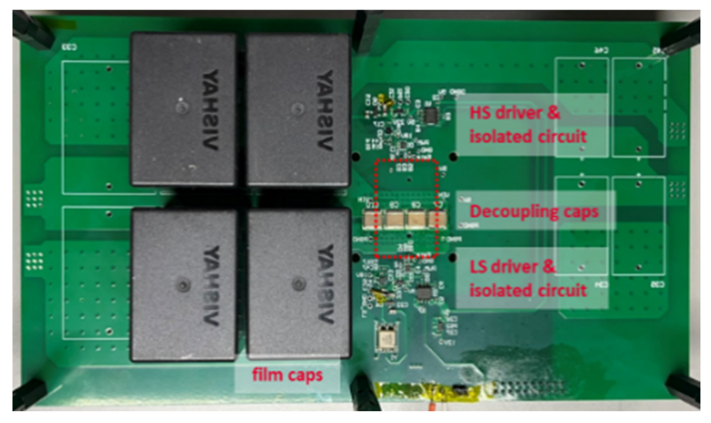
A double-pulse test (DPT) platform was constructed to evaluate the switching performance of the proposed module, as illustrated in
Figure 20. The half-bridge module is mounted on the reverse side of the test PCB, indicated by the dashed outline, and is considerably smaller than the surrounding circuitry. The high-frequency decoupling capacitors are assembled directly beneath the DC+ and DC− terminals to minimize the power-loop impedance during switching transients. The gate driver is UCC27614 from Texas Instruments, with a 10 A sink-source output current to provide sufficient current for fast turn-on and turn-off of the SiC MOSFET. The applied gate-drive voltages are 0 V for the off-state and +18 V for the on-state. The SiC device features an internal gate resistance of 3.5 Ω, and no additional external gate resistor is used in the test setup.
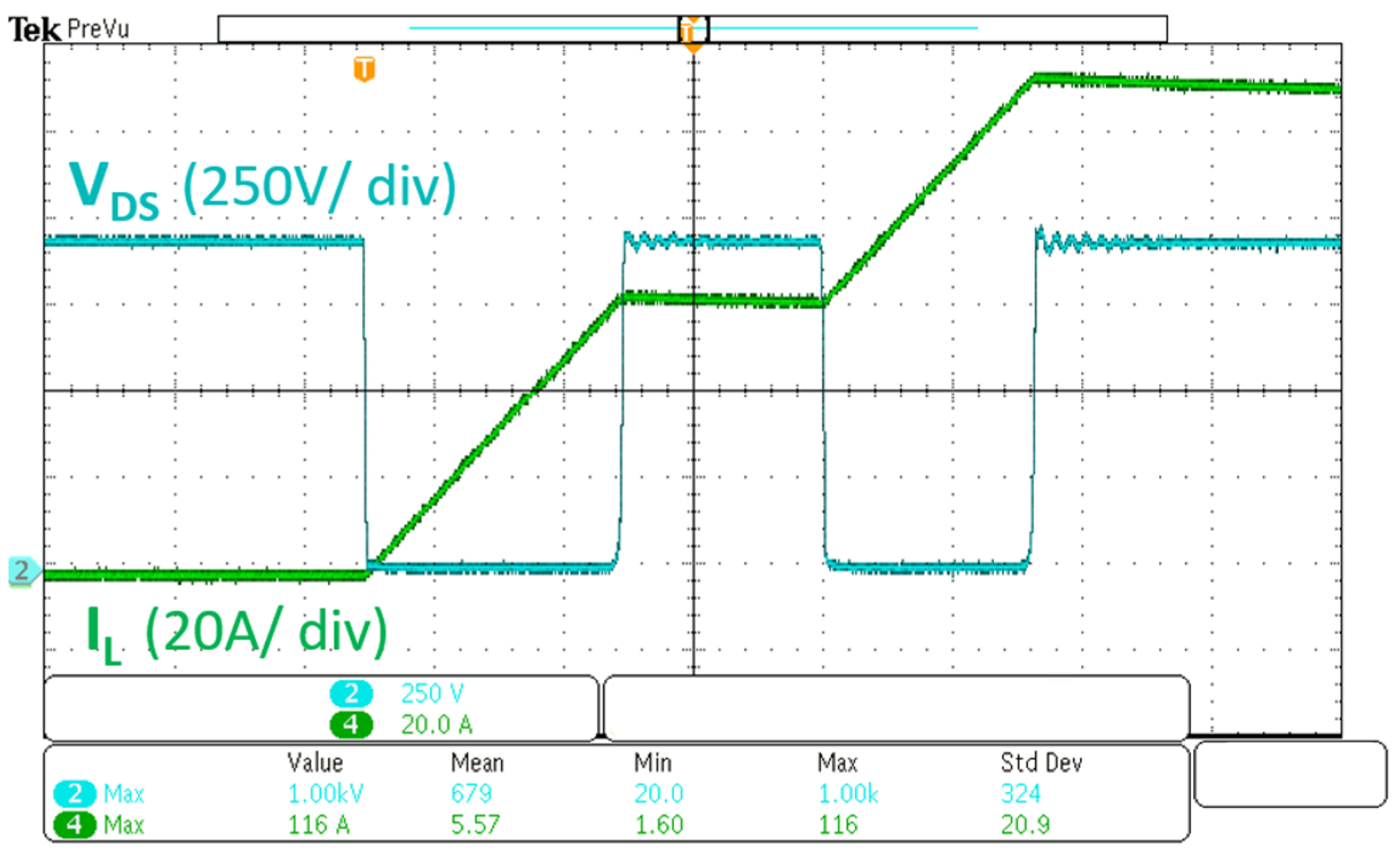
Figure 21 shows the DPT waveforms for a DC bus voltage equal to 950 V, which is 80% of the SiC MOSFET rated voltage. The peak current is 116 A. With proper power loop design and a small loop inductance, the overshoot is less than 30 V (around 3% of the bus voltage). The voltage probes used in this test have a bandwidth of 200 MHz. Based on the optimized loop, no high-frequency oscillation is observed.
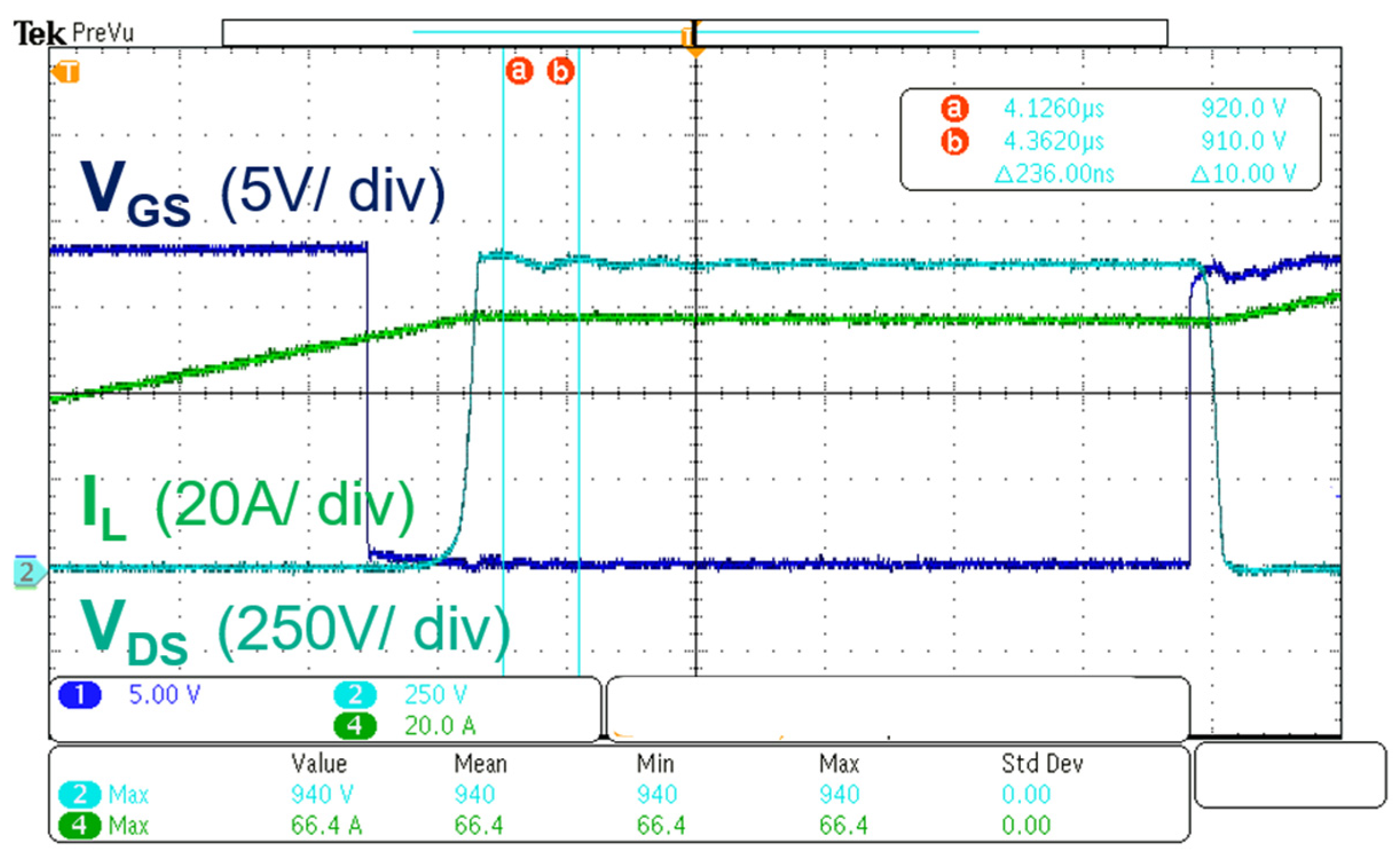
Figure 22 shows the waveforms of the MOSFET during the turn-off period. The oscillation frequency is 4.23 MHz due to the resonance of the ceramic decoupling capacitors and the power loop parasitic inductance.
Figure 23 shows the zoomed-in waveform, indicating that the proposed module achieves controlled switching speeds with dv/dt ≈ 17 V/ns during both turn-off and turn-on events. Despite the high bus voltage and >100 A current, the voltage overshoot remains <30 V, and the ringing is significantly damped. This behavior is attributed to the 3D-embedded structure, where the DC+ and DC− copper planes form a tightly coupled laminated pair that confines the switching current loop and minimizes parasitic inductance.
Furthermore, the minimized common-mode parasitic capacitance between the switching node and the heatsink reduces displacement currents generated by high dv/dt transitions. As a result, the structure inherently suppresses EMI emissions and reduces the stress on the gate driver and insulation system. These characteristics make the module suitable for fast-switching SiC applications requiring high dv/dt robustness.
8. Discussion
A novel, scalable, ultra-compact die-integrated PCB SiC half-bridge building block module has been designed and experimentally evaluated. The results presented in this work demonstrate the effectiveness of the die-integrated 3D PCB architecture in addressing the key limitations of conventional SiC power module packaging. Compared with a conventional DBC-based SiC half-bridge module, the proposed structure achieves a 95% reduction in physical volume and more than a 90% reduction in weight. The drastic reduction in both power-loop and gate-loop inductances highlights the advantage of employing vertically aligned copper planes within a compact laminated structure. These reductions translate directly into improved switching behavior, as evidenced by minimal voltage overshoot of less than 3% of the bus voltage and the absence of high-frequency oscillations during double-pulse testing. Owing to the symmetric PCB–die–PCB stack and the multilayer distribution of DC+, DC−, and switching-node planes, the replicated modules exhibit highly consistent parasitic parameters and extremely small mutual inductance. These characteristics naturally promote balanced current sharing, reducing the need for additional external busbar optimization or active balancing techniques. This makes the module architecture particularly attractive for applications that require multiple half-bridge units to be paralleled to achieve higher power ratings. The measured insulation withstand voltage, exceeding twice the rated bus voltage, confirms the structural reliability of the embedded layers, while the experimentally validated thermal distribution indicates that high-Tg copper-filled PCB laminates offer a promising path for high-temperature SiC operation. Both simulation and experimental results demonstrate that this die-integrated PCB half-bridge module could be an alternative for large-scale wide-bandgap power converters, offering low loop inductance, lower cost, ease of fabrication, and ease of power scale-up.
Author Contributions
Conceptualization, J.T. and W.-J.H.; methodology, J.T.; software, J.T. and W.-J.H.; validation, J.T. and W.-J.H.; formal analysis, J.T.; investigation, J.T. and Q.H.; resources, A.Q.H.; data curation, J.T.; writing—original draft preparation, J.T. and W.-J.H.; writing—review and editing, A.Q.H.; visualization, J.T. and Q.H.; supervision, A.Q.H.; project administration, A.Q.H. All authors have read and agreed to the published version of the manuscript.
Funding
This research was funded in part by Raytheon Technologies Corporation (“RTX”) under Award No. UTAUS-FA00000202, 1 December 2021–31 August 2022.
Data Availability Statement
The original contributions presented in this study are included in the article. Further inquiries can be directed to the corresponding author.
Conflicts of Interest
The authors declare no conflicts of interest.
References
- Wu, X.; Yang, X.; Ye, J.; Liu, G. Novel Prognostics for IGBTs Using Wire-Bond Contact Degradation Model Considering On-Chip Temperature Distribution. IEEE Trans. Power Electron. 2025, 40, 4411–4424. [Google Scholar] [CrossRef]
- Yin, S.; Tu, P.; Wang, P.; Tseng, K.J.; Qi, C.; Hu, X.; Zagrodnik, M.A.; Simanjorang, R. An Accurate Subcircuit Model of SiC Half-Bridge Module for Switching-Loss Optimization. IEEE Trans. Ind. Appl. 2017, 53, 3840–3848. [Google Scholar] [CrossRef]
- Tong, J.; Guo, Z.; Huang, A.Q. Design and Characterization of a Novel Transistor Outline (TO) Package With 3D Copper Frame. In Proceedings of the 2023 IEEE Energy Conversion Congress and Exposition (ECCE), Nashville, TN, USA, 29 October–2 November 2023; pp. 6069–6073. [Google Scholar] [CrossRef]
- Tong, J.; Huang, A.Q. Design and Characterization of a Novel Double-side Cooled Press-pack Packaging Structure. In Proceedings of the 2023 IEEE Energy Conversion Congress and Exposition (ECCE), Nashville, TN, USA, 29 October–2 November 2023; pp. 5480–5484. [Google Scholar] [CrossRef]
- Pascal, Y.; Abdedaim, A.; Labrousse, D.; Petit, M.; Lefebvre, S.; Costa, F. Using Laminated Metal Foam as the Top-Side Contact of a PCB-Embedded Power Die. IEEE Electron Device Lett. 2017, 38, 1453–1456. [Google Scholar] [CrossRef]
- Munding, A.; Kessler, A.; Scharf, T.; Plikat, B.; Pressel, K. Laminate Chip Embedding Technology—Impact of Material Choice and Processing for Very Thin Die Packaging. In Proceedings of the 2017 IEEE 67th Electronic Components and Technology Conference (ECTC), Orlando, FL, USA, 30 May–2 June 2017; pp. 711–718. [Google Scholar]
- Boettcher, L.; Karaszkiewicz, S.; Manessis, D.; Ostmann, A. Development of embedded power electronics modules. In Proceedings of the 2012 4th Electronic System-Integration Technology Conference, Amsterdam, The Netherlands, 17–20 September 2012; pp. 1–6. [Google Scholar]
- Hsu, W.-J.; Tong, J.; Huang, Q.; Huang, A.Q. Packaging and Characterization of an Ultra Compact 1200V PCB SiC MOSFET Half-Bridge Module. In Proceedings of the 2023 IEEE Applied Power Electronics Conference and Exposition (APEC), Orlando, FL, USA, 19–23 March 2023; pp. 2604–2608. [Google Scholar] [CrossRef]
- Hou, F.; Wang, W.; Ma, R.; Li, Y.; Han, Z.; Su, M.; Li, J.; Yu, Z.; Song, Y.; Wang, Q.; et al. Fan-Out Panel-Level PCB-Embedded SiC Power MOSFETs Packaging. IEEE J. Emerg. Sel. Top. Power Electron. 2020, 8, 367–380. [Google Scholar] [CrossRef]
- Knoll, J.; Son, G.; DiMarino, C.; Li, Q.; Stahr, H.; Morianz, M. Design and Analysis of a PCB-Embedded 1.2 kV SiC Half-Bridge Module. In Proceedings of the 2021 IEEE Energy Conversion Congress and Exposition (ECCE), Vancouver, BC, Canada, 10–14 October 2021; pp. 5240–5246. [Google Scholar]
- Khan, S.A.; Zhou, F.; Wang, M.; Le, D.; Chaturvedi, S. Bare-Die Embedding Technique for Highly Integrated Power Electronics for Small Mobility. IEEE Trans. Compon. Packag. Manuf. Technol. 2025, 15, 613–622. [Google Scholar] [CrossRef]
- Knoll, J.S.; Son, G.; DiMarino, C.; Li, Q.; Stahr, H.; Morianz, M. A PCB-Embedded 1.2 kV SiC MOSFET Half-Bridge Package for a 22 kW AC–DC Converter. IEEE Trans. Power Electron. 2022, 37, 11927–11936. [Google Scholar] [CrossRef]
- Cree. 1200 V, 16 mΩ All-Silicon Carbide Half-Bridge Module; CAB016M12FM3 Datasheet; Wolf Speed: Durham, NC, USA, 2021. [Google Scholar]
- STMicroelectronics. ACEPACK 2 Power Module, Fourpack Topology, 1200 V, 13 mΩ typ. SiC Power MOSFET gen.2 with NTC; A2F12M12W2-F1 Datasheet; STMicroelectronics: Geneva, Switzerland, 2022. [Google Scholar]
- Infineon. FF23MR12W1M1_B11 Datasheet; Infineon: Neubiberg, Germany, 2018. [Google Scholar]
- Feng, X.; Xiong, Q.; Gattozzi, A.; Montanari, G.C.; Seri, P.; Hebner, R. Cable commissioning and diagnostic tests: The effect of voltage supply frequency on partial discharge behavior. In Proceedings of the 2018 12th International Conference on the Properties and Applications of Dielectric Materials (ICPADM), Xi’an, China, 20–24 May 2018; pp. 373–376. [Google Scholar]
- Blackburn, D.L. Temperature measurements of semiconductor devices—A review. In Proceedings of the Twentieth Annual IEEE Semiconductor Thermal Measurement and Management Symposium (IEEE Cat. No.04CH37545), San Jose, CA, USA, 11 March 2004; pp. 70–80. [Google Scholar]
- Maximilian, S.; Elger, G. Measurement of the Transient Thermal Impedance of MOSFETs Over the Sensitivity of the Threshold Voltage. In Proceedings of the 2018 20th European Conference on Power Electronics and Applications (EPE’18 ECCE Europe), Riga, Latvia, 17–21 September 2018; pp. P.1–P.8. [Google Scholar]
- Mital, M.; Pang, Y.-F.; Scott, E.P. Evaluation of Thermal Resistance Matrix Method for an Embedded Power Electronic Module. IEEE Trans. Compon. Packag. Technol. 2008, 31, 382–387. [Google Scholar] [CrossRef]
Figure 1.
Exploded 3D view of the die-integrated PCB half-bridge building block module.
Figure 1.
Exploded 3D view of the die-integrated PCB half-bridge building block module.
Figure 2.
Front and back side views of the three PCBs: (a) top PCB, (b) connector PCB, (c) bottom PCB.
Figure 2.
Front and back side views of the three PCBs: (a) top PCB, (b) connector PCB, (c) bottom PCB.
Figure 3.
SiC MOSFET die topside view (size: 4960 μm × 4960 μm).
Figure 3.
SiC MOSFET die topside view (size: 4960 μm × 4960 μm).
Figure 4.
Copper-filled vias.
Figure 4.
Copper-filled vias.
Figure 5.
Proposed half-bridge module (a) compared to TO-247 package, (b) thickness compared to quarter coin, (c) total weight of the module is 0.06 oz.
Figure 5.
Proposed half-bridge module (a) compared to TO-247 package, (b) thickness compared to quarter coin, (c) total weight of the module is 0.06 oz.
Figure 6.
Pin out of the proposed half-bridge modules.
Figure 6.
Pin out of the proposed half-bridge modules.
Figure 7.
I-V curve of the LS MOSFET in the module, Vgs = 18 V, room temperature.
Figure 7.
I-V curve of the LS MOSFET in the module, Vgs = 18 V, room temperature.
Figure 8.
High-Pot insulation test setup and result of DC+ to DC− in the air at 2.76 kV.
Figure 8.
High-Pot insulation test setup and result of DC+ to DC− in the air at 2.76 kV.
Figure 9.
High-voltage high-frequency sinusoidal waveform PD test platform.
Figure 9.
High-voltage high-frequency sinusoidal waveform PD test platform.
Figure 10.
PD pattern diagram of the proposed package at AC 60 Hz, 2.26 kVrms voltage.
Figure 10.
PD pattern diagram of the proposed package at AC 60 Hz, 2.26 kVrms voltage.
Figure 11.
PD record with time for the proposed package at AC 60 Hz, 2.26 kVrms voltage.
Figure 11.
PD record with time for the proposed package at AC 60 Hz, 2.26 kVrms voltage.
Figure 12.
Package thermal resistance (θJC) simulation model structure.
Figure 12.
Package thermal resistance (θJC) simulation model structure.
Figure 13.
Thermal resistance (θJC) SolidWorks Flow simulation result: (a) surface attached to the test board, (b) package open view, (c) side view from the top.
Figure 13.
Thermal resistance (θJC) SolidWorks Flow simulation result: (a) surface attached to the test board, (b) package open view, (c) side view from the top.
Figure 14.
Body diode forward voltage thermal calibration (a) test setup, (b) Body diode forward voltage change over temperature at Vgs = −5V.
Figure 14.
Body diode forward voltage thermal calibration (a) test setup, (b) Body diode forward voltage change over temperature at Vgs = −5V.
Figure 15.
(a) Exploded 3D view of the proposed package copper structure. (b) Proposed package PCB layout.
Figure 15.
(a) Exploded 3D view of the proposed package copper structure. (b) Proposed package PCB layout.
Figure 16.
Parasitic inductance simulation schematic and the Q3D simulation model of the half-bridge module gate loop and power loop.
Figure 16.
Parasitic inductance simulation schematic and the Q3D simulation model of the half-bridge module gate loop and power loop.
Figure 17.
Parasitic inductance simulation results.
Figure 17.
Parasitic inductance simulation results.
Figure 18.
Single-module cross-view and current-flow direction.
Figure 18.
Single-module cross-view and current-flow direction.
Figure 19.
Exploded view of the proposed PCB-embedded SiC module array and planar bus structure.
Figure 19.
Exploded view of the proposed PCB-embedded SiC module array and planar bus structure.
Figure 20.
Bottom view of the DPT evaluation board with the half-bridge module on the other side.
Figure 20.
Bottom view of the DPT evaluation board with the half-bridge module on the other side.
Figure 21.
DPT results of MOSFET under 950 V/116 A.
Figure 21.
DPT results of MOSFET under 950 V/116 A.
Figure 22.
Turn-off waveforms of LS MOSFET DPT under 950 V/66 A.
Figure 22.
Turn-off waveforms of LS MOSFET DPT under 950 V/66 A.
Figure 23.
Zoom in for LS MOSFET DPT result under 950 V/66 A (a) Second pulse turn-on. (b) Second pulse turn-off.
Figure 23.
Zoom in for LS MOSFET DPT result under 950 V/66 A (a) Second pulse turn-on. (b) Second pulse turn-off.
Table 1.
Specifications of the developed module.
Table 1.
Specifications of the developed module.
| Parameter | Value |
|---|
| Packaging | Half-bridge |
| Voltage rating | 1200 V |
| On-resistance | 17 mΩ |
| Package insulation | None-insulated |
| Terminal insulation | DC+ to DC− 2 kV in air |
| Thickness | 1.0 mm |
| Module size | 20.3 mm × 31.1 mm |
| Cooling function | Single-sided cooling |
| Thermal resistance, junction to case | 0.41 °C/W |
| Power loop inductance | 2.2 nH (94% reduction compared with TO-247 half-bridge [10]) |
| Gate loop inductance | 3.8 nH (89% reduction compared with TO-247 half-bridge [10]) |
| Soldering peak body temperature | 250 °C |
| Module weight | 0.06 oz (90% reduction compared with DBC-stacked half-bridge module [13,14,15]) |
Table 2.
Package parasitic capacitance.
Table 2.
Package parasitic capacitance.
| Package Parasitic Capacitance | DC+ to SW | SW to DC− | HG to DC+ | HG to SW | LG to SW | LG to DC− |
|---|
| Capacitance Value | 30.9 pF | 12.6 pF | 0.15 pF | 0.59 pF | 0.15 pF | 0.6 pF |
| Disclaimer/Publisher’s Note: The statements, opinions and data contained in all publications are solely those of the individual author(s) and contributor(s) and not of MDPI and/or the editor(s). MDPI and/or the editor(s) disclaim responsibility for any injury to people or property resulting from any ideas, methods, instructions or products referred to in the content. |
